

Datasheet GS8662R08-333, GS8662R09-333, GS8662R18-333, GS8662R36E-333, GS8662R08-300 Datasheet (GSI TECHNOLOGY)
...Page 1
Preliminary
GS8662R08/09/18/36E-333/300/250/200/167
165-Bump BGA
72Mb SigmaCIO DDR-II
Commercial Temp
Industrial Temp
Burst of 4 SRAM
Features
• Simultaneous Read and Write SigmaCIO™ Interface
• Common I/O bus
• JEDEC-standard pinout and package
• Double Data Rate interface
• Byte Write (x36 and x18) and Nybble Write (x8) function
• Burst of 4 Read and Write
• 1.8 V +100/–100 mV core power supply
• 1.5 V or 1.8 V HSTL Interface
• Pipelined read operation with self-timed Late Write
• Fully coherent read and write pipelines
• ZQ pin for programmable output drive strength
• IEEE 1149.1 JTAG-compliant Boundary Scan
• Pin-compatible with present 9Mb, 18Mb, 36Mb and future
144Mb devices
• 165-bump, 15 mm x 17 mm, 1 mm bump pitch BGA package
• RoHS-compliant 165-bump BGA package available
SigmaCIO™ Family Overview
The GS8662R08/09/18/36E are built in compliance with the
SigmaCIO DDR-II SRAM pinout standard for Common I/O
synchronous SRAMs. They are 75,497,472-bit (72Mb)
SRAMs. The GS8662R08/09/18/36E SigmaCIO SRAMs are
just one element in a family of low power, low voltage HSTL
I/O SRAMs designed to operate at the speeds needed to
implement economical high performance networking systems.
Clocking and Addressing Schemes
The GS8662R08/09/18/36E SigmaCIO DDR-II SRAMs are
synchronous devices. They employ two input register clock
inputs, K and
inputs, not differential inputs to a single differential clock input
buffer. The device also allows the user to manipulate the
output register clock inputs quasi independently with the C and
C clock inputs. C and
K. K and K are independent single-ended clock
C are also independent single-ended
333 MHz–167 MHz
1.8 V V
DD
1.8 V and 1.5 V I/O
Bottom View
165-Bump, 15 mm x 17 mm BGA
1 mm Bump Pitch, 11 x 15 Bump Array
clock inputs, not differential inputs. If the C clocks are tied
high, the K clocks are routed internally to fire the output
registers instead.
Common I/O x36 and x18 SigmaCIO DDR-II B4 RAMs
always transfer data in four packets. When a new address is
loaded, A0 and A1 preset an internal 2 bit linear address
counter. The counter increments by 1 for each beat of a burst of
four data transfer. The counter always wraps to 00 after
reaching 11, no matter where it starts.
Common I/O x8 SigmaCIO DDR-II B4 RAMs always transfer
data in four packets. When a new address is loaded, the LSBs
are internally set to 0 for the first read or write transfer, and
incremented by 1 for the next 3 transfers. Because the LSBs
are tied off internally, the address field of a x8 SigmaCIO
DDR-II B4 RAM is always two address pins less than the
advertised index depth (e.g., the 4M x 18 has a 1024K
addressable index).
Parameter Synopsis
-333 -300 -250 -200 -167
tKHKH 3.0 ns 3.3 ns 4.0 ns 5.0 ns 6.0 ns
tKHQV 0.45 ns 0.45 ns 0.45 ns 0.45 ns 0.5 ns
Rev: 1.01 9/2005 1/37 © 2005, GSI Technology
Specifications cited are subject to change without notice. For latest documentation see http://www.gsitechnology.com.
Page 2
Preliminary
GS8662R08/09/18/36E-333/300/250/200/167
2M x 36 SigmaCIO DDR-II SRAM—Top View
1 2 3 4 5 6 7 8 9 10 11
A CQ
MCL/SA
(144Mb)
SA R/W BW2 K BW1 LD SA SA CQ
B NC DQ27 DQ18 SA BW3 K BW0 SA NC NC DQ8
C NC NC DQ28 V
D NC DQ29 DQ19 V
E NC NC DQ20 V
F NC DQ30 DQ21 V
G NC DQ31 DQ22 V
H Doff V
REF
V
DDQ
V
J NC NC DQ32 V
K NC NC DQ23 V
L NC DQ33 DQ24 V
M NC NC DQ34 V
SS
SS
DDQ
DDQ
DDQ
DDQ
DDQ
DDQ
DDQ
SS
SA SA0 SA1 V
V
SS
V
SS
V
DD
V
DD
V
DD
V
DD
V
DD
V
SS
V
SS
V
SS
V
SS
V
SS
V
SS
V
SS
V
SS
V
SS
V
SS
V
SS
V
SS
V
SS
V
DD
V
DD
V
DD
V
DD
V
DD
V
SS
V
SS
SS
V
SS
V
DDQ
V
DDQ
V
DDQ
V
DDQ
V
DDQ
V
DDQ
V
DDQ
V
SS
NC DQ17 DQ7
NC NC DQ16
NC DQ15 DQ6
NC NC DQ5
NC NC DQ14
V
DDQ
V
REF
NC DQ13 DQ4
NC DQ12 DQ3
NC NC DQ2
NC DQ11 DQ1
ZQ
N NC DQ35 DQ25 V
SS
SA SA SA V
SS
NC NC DQ10
P NC NC DQ26 SA SA C SA SA NC DQ9 DQ0
R TDO TCK SA SA SA C SA SA SA TMS TDI
11 x 15 Bump BGA—13 x 15 mm2 Body—1 mm Bump Pitch
Notes:
1. BW0 controls writes to DQ0:DQ8; BW1 controls writes to DQ9:DQ17; BW2 controls writes to DQ18:DQ26; BW3 controls writes to
DQ27:DQ35
2. MCL = Must Connect Low
Rev: 1.01 9/2005 2/37 © 2005, GSI Technology
Specifications cited are subject to change without notice. For latest documentation see http://www.gsitechnology.com.
Page 3
Preliminary
GS8662R08/09/18/36E-333/300/250/200/167
4M x 18 SigmaCIO DDR-II SRAM—Top View
1 2 3 4 5 6 7 8 9 10 11
A CQ SA SA R/W BW1 K NC LD SA SA CQ
B NC DQ9 NC SA NC K BW0 SA NC NC DQ8
C NC NC NC V
D NC NC DQ10 V
E NC NC DQ11 V
F NC DQ12 NC V
G NC NC DQ13 V
H Doff V
REF
V
DDQ
V
J NC NC NC V
K NC NC DQ14 V
L NC DQ15 NC V
M NC NC NC V
N NC NC DQ16 V
SS
SS
DDQ
DDQ
DDQ
DDQ
DDQ
DDQ
DDQ
SS
SS
SA SA0 SA1 V
V
SS
V
SS
V
DD
V
DD
V
DD
V
DD
V
DD
V
SS
V
SS
V
SS
V
SS
V
SS
V
SS
V
SS
V
SS
V
SS
V
SS
V
SS
V
SS
V
SS
V
DD
V
DD
V
DD
V
DD
V
DD
V
SS
V
SS
SA SA SA V
SS
V
SS
V
DDQ
V
DDQ
V
DDQ
V
DDQ
V
DDQ
V
DDQ
V
DDQ
V
SS
SS
NC DQ7 NC
NC NC NC
NC NC DQ6
NC NC DQ5
NC NC NC
V
DDQ
V
REF
NC DQ4 NC
NC NC DQ3
NC NC DQ2
NC DQ1 NC
NC NC NC
ZQ
P NC NC DQ17 SA SA C SA SA NC NC DQ0
R TDO TCK SA SA SA C SA SA SA TMS TDI
11 x 15 Bump BGA—13 x 15 mm2 Body—1 mm Bump Pitch
Notes:
1. BW0 controls writes to DQ0:DQ8; BW1 controls writes to DQ9:DQ17
2. MCL = Must Connect Low
Rev: 1.01 9/2005 3/37 © 2005, GSI Technology
Specifications cited are subject to change without notice. For latest documentation see http://www.gsitechnology.com.
Page 4

Preliminary
GS8662R08/09/18/36E-333/300/250/200/167
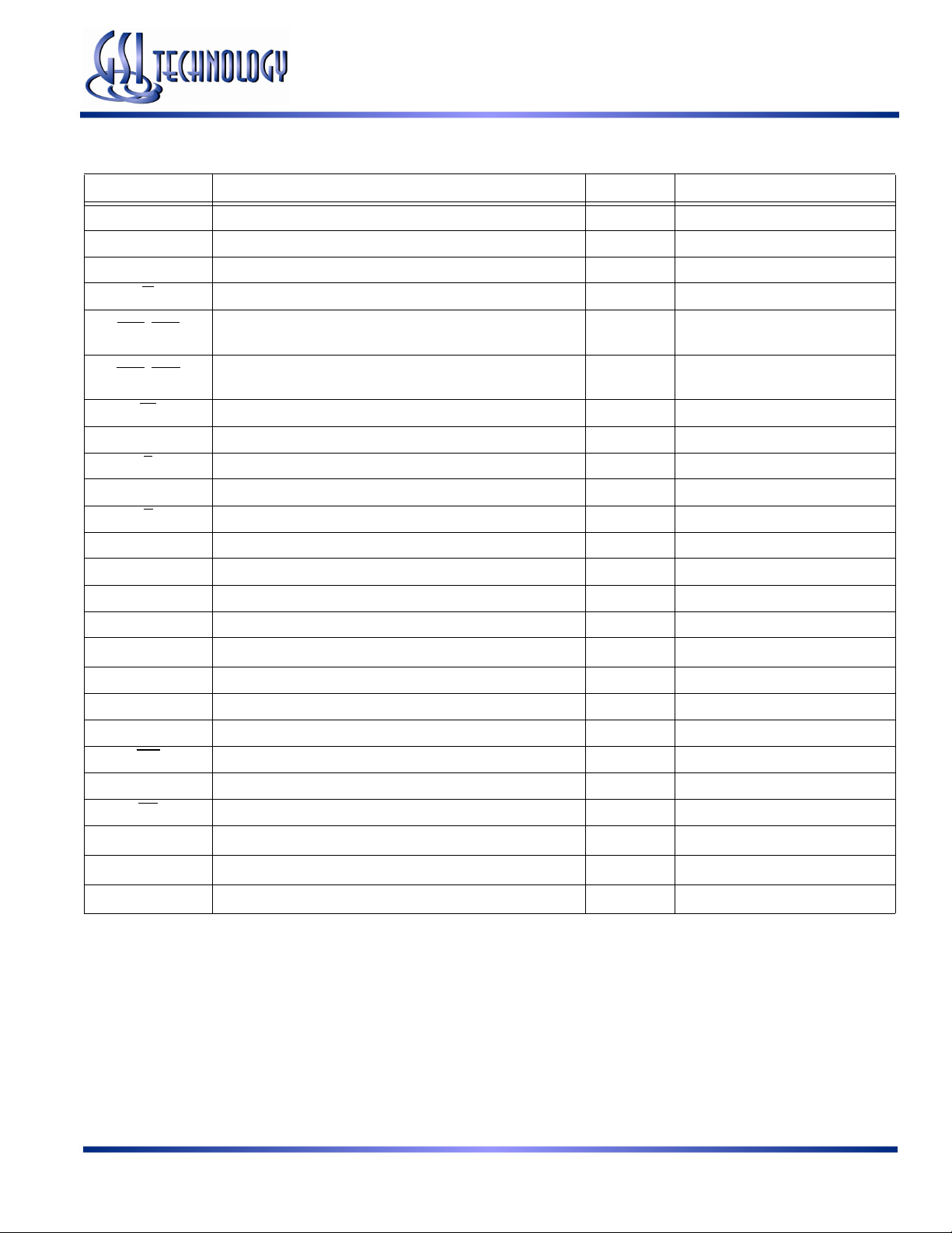
8M x 9 SigmaCIO DDR-II SRAM—Top View
1 2 3 4 5 6 7 8 9 10 11
A CQ SA SA R/W NC K NC LD SA SA CQ
B NC NC NC SA NC K BW SA NC NC DQ4
C NC NC NC V
D NC NC NC V
E NC NC DQ5 V
F NC NC NC V
G NC NC DQ6 V
H Doff V
REF
V
DDQ
V
J NC NC NC V
K NC NC NC V
L NC DQ7 NC V
M NC NC NC V
N NC NC NC V
SS
SS
DDQ
DDQ
DDQ
DDQ
DDQ
DDQ
DDQ
SS
SS
SA NC SA V
V
SS
V
SS
V
DD
V
DD
V
DD
V
DD
V
DD
V
SS
V
SS
V
SS
V
SS
V
SS
V
SS
V
SS
V
SS
V
SS
V
SS
V
SS
V
SS
V
SS
V
DD
V
DD
V
DD
V
DD
V
DD
V
SS
V
SS
SA SA SA V
SS
V
SS
V
DDQ
V
DDQ
V
DDQ
V
DDQ
V
DDQ
V
DDQ
V
DDQ
V
SS
SS
NC NC NC
NC NC NC
NC NC DQ3
NC NC NC
NC NC NC
V
DDQ
V
REF
NC DQ2 NC
NC NC NC
NC NC DQ1
NC NC NC
NC NC NC
ZQ
P NC NC DQ8 SA SA C SA SA NC NC DQ0
R TDO TCK SA SA SA C SA SA SA TMS TDI
11 x 15 Bump BGA—13 x 15 mm2 Body—1 mm Bump Pitch
Notes:
1. Unlike the x36 and x18 versions of this device, the x8 and x9 versions do not give the user access to A0 and A1. SA0 and SA1 are set to
0 at the beginning of each access.
2. MCL = Must Connect Low
Rev: 1.01 9/2005 4/37 © 2005, GSI Technology
Specifications cited are subject to change without notice. For latest documentation see http://www.gsitechnology.com.
Page 5

Preliminary
GS8662R08/09/18/36E-333/300/250/200/167
8M x 8 SigmaCIO DDR-II SRAM—Top View
1 2 3 4 5 6 7 8 9 10 11
A CQ SA SA R/W NW1 K NC LD SA SA CQ
B NC NC NC SA NC K NW0 SA NC NC DQ3
C NC NC NC V
D NC NC NC V
E NC NC DQ4 V
F NC NC NC V
G NC NC DQ5 V
H Doff V
REF
V
DDQ
V
J NC NC NC V
K NC NC NC V
L NC DQ6 NC V
M NC NC NC V
N NC NC NC V
SS
SS
DDQ
DDQ
DDQ
DDQ
DDQ
DDQ
DDQ
SS
SS
SA NC SA V
V
SS
V
SS
V
DD
V
DD
V
DD
V
DD
V
DD
V
SS
V
SS
V
SS
V
SS
V
SS
V
SS
V
SS
V
SS
V
SS
V
SS
V
SS
V
SS
V
SS
V
DD
V
DD
V
DD
V
DD
V
DD
V
SS
V
SS
SA SA SA V
SS
V
SS
V
DDQ
V
DDQ
V
DDQ
V
DDQ
V
DDQ
V
DDQ
V
DDQ
V
SS
SS
NC NC NC
NC NC NC
NC NC DQ2
NC NC NC
NC NC NC
V
DDQ
V
REF
NC DQ1 NC
NC NC NC
NC NC DQ0
NC NC NC
NC NC NC
ZQ
P NC NC DQ7 SA SA C SA SA NC NC NC
R TDO TCK SA SA SA C SA SA SA TMS TDI
11 x 15 Bump BGA—13 x 15 mm2 Body—1 mm Bump Pitch
Notes:
1. Unlike the x36 and x18 versions of this device, the x8 and x9 versions do not give the user access to A0 and A1. SA0 and SA1 are set to
0 at the beginning of each access.
2. NW0 controls writes to DQ0:DQ3; NW1 controls writes to DQ4:DQ7
3. MCL = Must Connect Low
Rev: 1.01 9/2005 5/37 © 2005, GSI Technology
Specifications cited are subject to change without notice. For latest documentation see http://www.gsitechnology.com.
Page 6
GS8662R08/09/18/36E-333/300/250/200/167
Pin Description Table
Symbol Description Type Comments
SA Synchronous Address Inputs Input —
NC No Connect — —
R Synchronous Read Input Active High
W Synchronous Write Input Active Low
BW0–BW3 Synchronous Byte Writes Input
NW0–NW1 Nybble Write Control Pin Input
LD Synchronous Load Pin Input Active Low
K Input Clock Input Active High
K Input Clock Input Active Low
C Output Clock Input Active High
C Output Clock Input Active Low
TMS Test Mode Select Input —
Preliminary
Active Low
x18/x36 only
Active Low
x8 only
TDI Test Data Input Input —
TCK Test Clock Input Input —
TDO Test Data Output Output —
V
REF
ZQ Output Impedance Matching Input Input —
MCL Must Connect Low — —
DQ Data I/O Input/Output Three State
Doff Disable DLL when low Input Active Low
CQ Output Echo Clock Output —
CQ Output Echo Clock Output —
V
DD
V
DDQ
V
SS
Note:
NC = Not Connected to die or any other pin
HSTL Input Reference Voltage Input —
Isolated Output Buffer Supply Supply 1.5 V Nominal
Power Supply Supply 1.8 V Nominal
Power Supply: Ground Supply —
Rev: 1.01 9/2005 6/37 © 2005, GSI Technology
Specifications cited are subject to change without notice. For latest documentation see http://www.gsitechnology.com.
Page 7

Preliminary
GS8662R08/09/18/36E-333/300/250/200/167
Background
Common I/O SRAMs, from a system architecture point of view, are attractive in read dominated or block transfer applications.
Therefore, the SigmaCIO DDR-II SRAM interface and truth table are optimized for burst reads and writes. Common I/O SRAMs
are unpopular in applications where alternating reads and writes are needed because bus turnaround delays can cut high speed
Common I/O SRAM data bandwidth in half.
Burst Operations
Read and write operations are “burst” operations. In every case where a read or write command is accepted by the SRAM, it will
respond by issuing or accepting four beats of data, executing a data transfer on subsequent rising edges of K and K#, as illustrated
in the timing diagrams. It is not possible to stop a burst once it starts. Four beats of data are always transferred. This means that it is
possible to load new addresses every other K clock cycle. Addresses can be loaded less often, if intervening deselect cycles are
inserted.
Deselect Cycles
Chip Deselect commands are pipelined to the same degree as read commands. This means that if a deselect command is applied to
the SRAM on the next cycle after a read command captured by the SRAM, the device will complete the four beat read data transfer
and then execute the deselect command, returning the output drivers to high-Z.A high on the LD# pin prevents the RAM from
loading read or write command
inputs and puts the RAM into deselect mode as soon as it completes all outstanding burst transfer operations.
SigmaCIO DDR-II B4 SRAM Read Cycles
The status of the Address, LD# and R/W# pins are evaluated on the rising edge of K. Because the device executes a four beat burst
transfer in
response to a read command, if the previous command captured was a read or write command, the Address, LD# and R/W# pins
are ignored. If the previous command captured was a deselect, the control pin status is checked.The SRAM executes pipelined
reads. The read command is clocked into the SRAM by a rising edge of K. After the next rising edge of K, the SRAM produces
data out in response to the next rising edge of C# (or the next rising edge of K#, if C and C# are tied high). The second beat of data
is transferred on the next rising edge of C, then on the next rising edge of C# and finally on the next rising edge of C, for a total of
four transfers per address load.
SigmaCIO DDR-II B4 SRAM Write Cycles
The status of the Address, LD# and R/W# pins are evaluated on the rising edge of K. Because the device executes a four beat burst
transfer in response to a write command, if the previous command captured was a read or write command, the Address, LD# and R/
W# pins are ignored at the next rising edge of K. If the previous command captured was a deselect, the control pin status is
checked.The SRAM executes “late write” data transfers. Data in is due at the device inputs on the rising edge of K following the
rising edge of K clock used to clock in the write command and the write address. To complete the remaining three beats of the burst
of four write transfer the SRAM captures data in on the next rising edge of K#, the following rising edge of K and finally on the
next rising edge of K#, for a total of four transfers per address load.
Rev: 1.01 9/2005 7/37 © 2005, GSI Technology
Specifications cited are subject to change without notice. For latest documentation see http://www.gsitechnology.com.
Page 8
GS8662R08/09/18/36E-333/300/250/200/167
Power-Up Sequence for SigmaQuad-II SRAMs
SigmaQuad-II SRAMs must be powered-up in a specific sequence in order to avoid undefined operations.
Power-Up Sequence
1. Power-up and maintain Doff at low state.
1a. Apply VDD.
1b. Apply V
1c. Apply V
2. After power is achieved and clocks (K, K, C, C) are stablized, change Doff to high.
3. An additional 1024 clock cycles are required to lock the DLL after it has been enabled.
Note:
If you want to tie Doff high with an unstable clock, you must stop the clock for a minimum of 30 seconds to reset the DLL after the clocks become
stablized.
DLL Constraints
• The DLL synchronizes to either K or C clock. These clocks should have low phase jitter (t
• The DLL cannot operate at a frequency lower than 119 MHz.
• If the incoming clock is not stablized when DLL is enabled, the DLL may lock on the wrong frequency and cause undefined errors or failures during
the initial stage.
Power UP Interval Unstable Clocking Interval DLL Locking Interval (1024 Cycles) Normal Operation
.
DDQ
(may also be applied at the same time as V
REF
Power-Up Sequence (Doff controlled)
DDQ
).
on page 20).
KCVar
Preliminary
K
K
V
DD
V
DDQ
V
REF
Doff
Power-Up Sequence (Doff tied High)
Power UP Interval Unstable Clocking Interval Stop Clock Interval DLL Locking Interval (1024 Cycles) Normal Operation
K
K
V
DD
V
DDQ
30ns Min
V
REF
Doff
Note:
If the frequency is changed, DLL reset is required. After reset, a minimum of 1024 cycles is required for DLL lock.
Rev: 1.01 9/2005 8/37 © 2005, GSI Technology
Specifications cited are subject to change without notice. For latest documentation see http://www.gsitechnology.com.
Page 9

Preliminary
GS8662R08/09/18/36E-333/300/250/200/167
Special Functions
Byte Write and Nybble Write Control
Byte Write Enable pins are sampled at the same time that Data In is sampled. A high on the Byte Write Enable pin associated with
a particular byte (e.g.,
stored at the current address at that byte location undisturbed. Any or all of the Byte Write Enable pins may be driven high or low
during the data in sample times in a write sequence.
Each write enable command and write address loaded into the RAM provides the base address for a 4 beat data transfer. The x18
version of the RAM, for example, may write 72 bits in association with each address loaded. Any 9-bit byte may be masked in any
write sequence.
Nybble Write (4-bit) write control is implemented on the 8-bit-wide version of the device. For the x8 version of the device,
“Nybble Write Enable” and “
Example x18 RAM Write Sequence using Byte Write Enables
BW0 controls D0–D8 inputs) will inhibit the storage of that particular byte, leaving whatever data may be
NBx” may be substituted in all the discussion above.
Data In Sample
Time
Beat 1 0 1 Data In Don’t Care
Beat 2 1 0 Don’t Care Data In
Beat 3 0 0 Data In Data In
Beat 4 1 0 Don’t Care Data In
BW0 BW1 D0–D8 D9–D17
Resulting Write Operation
Byte 1
D0–D8
Written Unchanged Unchanged Written Written Written Unchanged Written
Output Register Control
SigmaCIO DDR-II SRAMs offer two mechanisms for controlling the output data registers. Typically, control is handled by the
Output Register Clock inputs, C and
of the output registers by allowing the user to delay driving data out as much as a few nanoseconds beyond the next rising edges of
the K and
RAM to function as a conventional pipelined read SRAM.
K clocks. If the C and C clock inputs isare tied high, the RAM reverts to K and K control of the outputs, allowing the
Byte 2
D9–D17
Beat 1 Beat 2 Beat 3 Beat 4
Byte 1
D0–D8
C. The Output Register Clock inputs can be used to make small phase adjustments in the firing
Byte 2
D9–D17
Byte 1
D0–D8
Byte 2
D9–D17
Byte 1
D0–D8
Byte 2
D9–D17
Rev: 1.01 9/2005 9/37 © 2005, GSI Technology
Specifications cited are subject to change without notice. For latest documentation see http://www.gsitechnology.com.
Page 10
LD
LD
LD
LD
R/W
A0–A
Preliminary
GS8662R08/09/18/36E-333/300/250/200/167
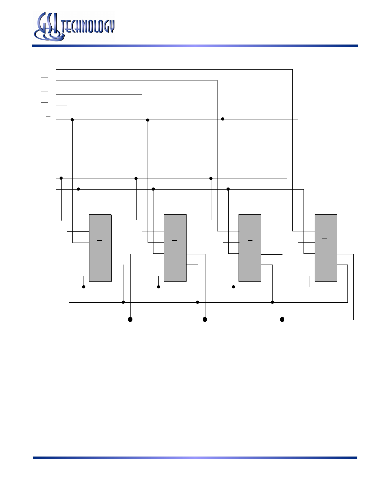
Example Four Bank Depth Expansion Schematic
3
2
1
0
n
K
C
DQ1–
CQ
Note:
For simplicity BWn
Bank 0
A
LD
R/W
CQ CQ CQ CQ
K
Bank 1 Bank 2
A
LD
A
LD
R/W R/W
K
K
Bank 3
A
LD
R/W
K
DQ DQ DQ DQ
CC CC
(or NWn), K, and C are not shown.
Rev: 1.01 9/2005 10/37 © 2005, GSI Technology
Specifications cited are subject to change without notice. For latest documentation see http://www.gsitechnology.com.
Page 11
Preliminary
GS8662R08/09/18/36E-333/300/250/200/167
FLXDrive-II Output Driver Impedance Control
HSTL I/O SigmaCIO DDR-II SRAMs are supplied with programmable impedance output drivers. The ZQ pin must be connected
to V
via an external resistor, RQ, to allow the SRAM to monitor and adjust its output driver impedance. The value of RQ must be
SS
5X the value of the desired RAM output impedance. The allowable range of RQ to guarantee impedance matching continuously is
between 150Ω and 300Ω. Periodic readjustment of the output driver impedance is necessary as the impedance is affected by drifts
in supply voltage and temperature. The SRAM’s output impedance circuitry compensates for drifts in supply voltage and
temperature. A clock cycle counter periodically triggers an impedance evaluation, resets and counts again. Each impedance
evaluation may move the output driver impedance level one step at a time towards the optimum level. The output driver is
implemented with discrete binary weighted impedance steps. Updates of pull-down drive impedance occur whenever a driver is
producing a “1” or is High-Z. Pull-up drive impedance is updated when a driver is producing a “0” or is High-Z.
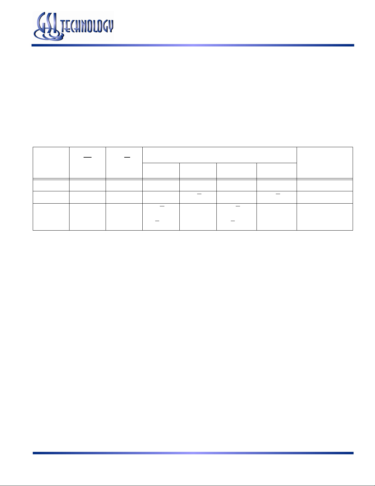
Common I/O SigmaCIO DDR-II B4 SRAM Truth Table
DQ
K
n
↑ 1 X Hi-Z Hi-Z Hi-Z Hi-Z Deselect
LD R/W
Operation
A + 0 A + 1 A + 2 A + 3
↑ 0 0 D@K
↑ 0 1
Note:
Q is controlled by K clocks if C clocks are not used.
Q@K
or
C
n+1
n+1
n+1
D@K
Q@K
or
C
n+2
n+1
n+2
D@K
Q@K
or
C
n+2
n+2
n+2
D@K
Q@K
or
C
n+3
n+2
n+3
Write
Read
Rev: 1.01 9/2005 11/37 © 2005, GSI Technology
Specifications cited are subject to change without notice. For latest documentation see http://www.gsitechnology.com.
Page 12
Preliminary
GS8662R08/09/18/36E-333/300/250/200/167
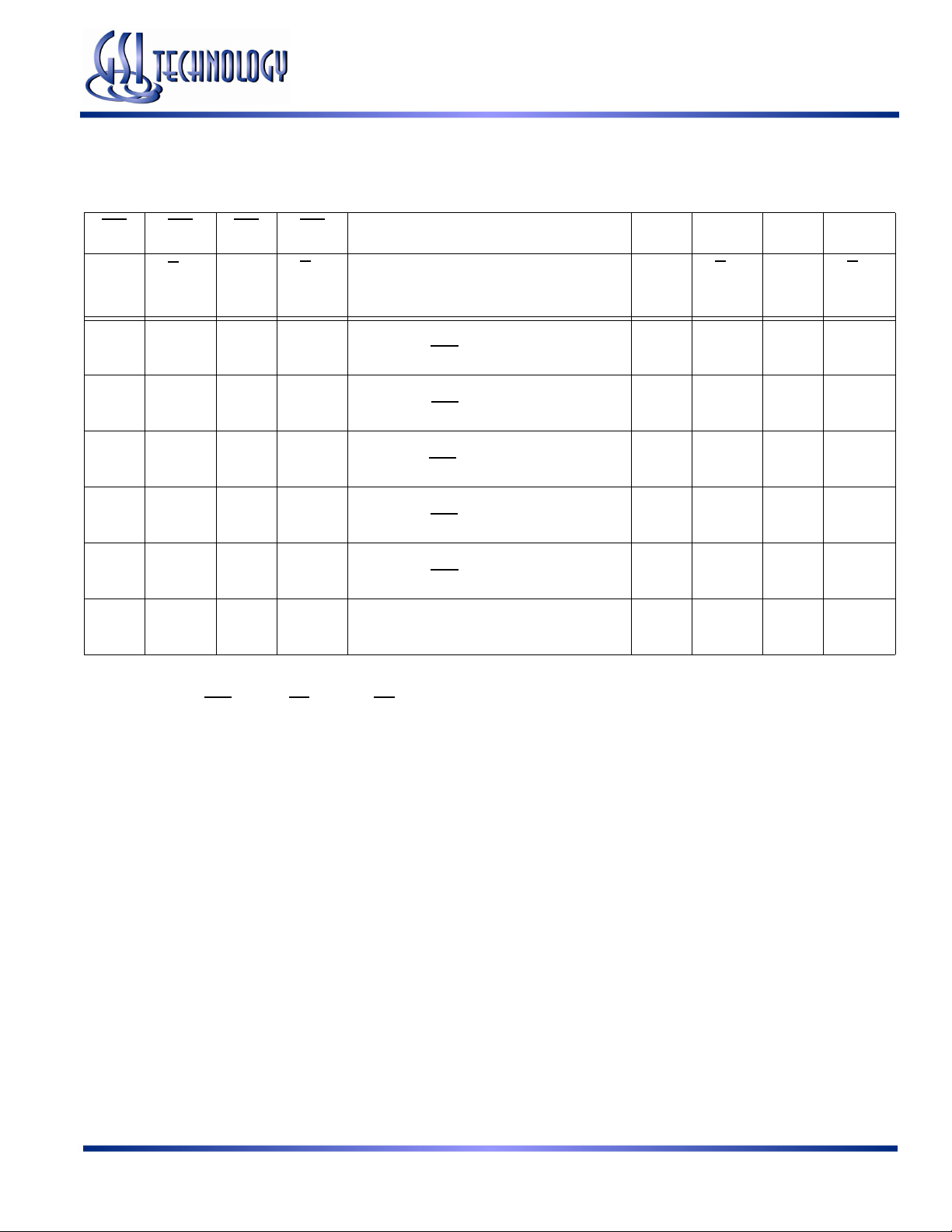
B4 Byte Write Clock Truth Table
BW BW BW BW Current Operation D D D D
K ↑
(t
n+1
T T T T
T F F F
F T F F
F F T F
F F F T
F F F F
Notes:
1. “1” = input “high”; “0” = input “low”; “X” = input “don’t care”; “T” = input “true”; “F” = input “false”.
2. If one or more BWn = 0, then BW = “T”, else BW = “F”.
K ↑
(t
)
n+1½
K ↑
)
(t
n+2
K ↑
)
(t
)
n+2½
Dx stored if BWn = 0 in all four data transfers
Dx stored if BWn = 0 in 1st data transfer only
Dx stored if BWn = 0 in 2nd data transfer only
Dx stored if BWn = 0 in 3rd data transfer only
Dx stored if BWn = 0 in 4th data transfer only
No Dx stored in any of the four data transfers
K ↑
(tn)
Write
Write
Write
Write
Write
Write Abort
K ↑
(t
n+1
D0 D2 D3 D4
D0 X X X
X D1 X X
X X D2 X
X X X D3
X X X X
K ↑
)
(t
n+1½
K ↑
)
(t
)
n+2
(t
K ↑
n+2½
)
*Assuming stable conditions, the RAM can achieve optimum impedance within 1024 cycles.
Rev: 1.01 9/2005 12/37 © 2005, GSI Technology
Specifications cited are subject to change without notice. For latest documentation see http://www.gsitechnology.com.
Page 13

Preliminary
GS8662R08/09/18/36E-333/300/250/200/167
B4 Nybble Write Clock Truth Table
NW NW NW NW Current Operation D D D D
K ↑
(t
n+1
T T T T
T F F F
F T F F
F F T F
F F F T
F F F F
Notes:
1. “1” = input “high”; “0” = input “low”; “X” = input “don’t care”; “T” = input “true”; “F” = input “false”.
2. If one or more NWn = 0, then NW = “T”, else NW = “F”.
K ↑
)
(t
n+1½
K ↑
)
(t
n+2
K ↑
)
(t
)
n+2½
Dx stored if NWn = 0 in all four data transfers
Dx stored if NWn = 0 in 1st data transfer only
Dx stored if NWn = 0 in 2nd data transfer only
Dx stored if NWn = 0 in 3rd data transfer only
Dx stored if NWn = 0 in 4th data transfer only
No Dx stored in any of the four data transfers
K ↑
(tn)
Write
Write
Write
Write
Write
Write Abort
K ↑
(t
n+1
D0 D2 D3 D4
D0 X X X
X D1 X X
X X D2 X
X X X D3
X X X X
K ↑
)
(t
n+1½
K ↑
)
(t
)
n+2
(t
K ↑
n+2½
)
Rev: 1.01 9/2005 13/37 © 2005, GSI Technology
Specifications cited are subject to change without notice. For latest documentation see http://www.gsitechnology.com.
Page 14

GS8662R08/09/18/36E-333/300/250/200/167
x36 Byte Write Enable (BWn) Truth Table
BW0 BW1 BW2 BW3 D0–D8 D9–D17 D18–D26 D27–D35
1 1 1 1 Don’t Care Don’t Care Don’t Care Don’t Care
0 1 1 1 Data In Don’t Care Don’t Care Don’t Care
1 0 1 1 Don’t Care Data In Don’t Care Don’t Care
0 0 1 1 Data In Data In Don’t Care Don’t Care
1 1 0 1 Don’t Care Don’t Care Data In Don’t Care
0 1 0 1 Data In Don’t Care Data In Don’t Care
1 0 0 1 Don’t Care Data In Data In Don’t Care
0 0 0 1 Data In Data In Data In Don’t Care
1 1 1 0 Don’t Care Don’t Care Don’t Care Data In
0 1 1 0 Data In Don’t Care Don’t Care Data In
Preliminary
1 0 1 0 Don’t Care Data In Don’t Care Data In
0 0 1 0 Data In Data In Don’t Care Data In
1 1 0 0 Don’t Care Don’t Care Data In Data In
0 1 0 0 Data In Don’t Care Data In Data In
1 0 0 0 Don’t Care Data In Data In Data In
0 0 0 0 Data In Data In Data In Data In
x18 Byte Write Enable (BWn) Truth Table
BW0 BW1 D0–D8 D9–D17
1 1 Don’t Care Don’t Care
0 1 Data In Don’t Care
1 0 Don’t Care Data In
0 0 Data In Data In
x8 Nybble Write Enable (NWn) Truth Table
NW0 NW1 D0–D3 D4–D7
1 1 Don’t Care Don’t Care
0 1 Data In Don’t Care
1 0 Don’t Care Data In
0 0 Data In Data In
Rev: 1.01 9/2005 14/37 © 2005, GSI Technology
Specifications cited are subject to change without notice. For latest documentation see http://www.gsitechnology.com.
Page 15

GS8662R08/09/18/36E-333/300/250/200/167
B4 State Diagram
Power-Up
NOP
LOAD
Preliminary
LOAD
LOAD
Load New
Address
LOAD
READ WRITE
Read Address
READ WRITE
DDR Read DDR Write
Always
Increment
LOAD
LOAD
Always
Increment
Write Address
Notes:
1. The internal burst address counter is a 4-bit linear counter (i.e., when first address is A0, next internal burst address is A0+1).
2. “READ” refers to read active status with R/W
3. “LOAD” refers to read new address active status with LD
= High, “WRITE” refers to write inactive status with R/W = Low.
= Low, “LOAD” refers to read new address inactive status with LD = High.
Rev: 1.01 9/2005 15/37 © 2005, GSI Technology
Specifications cited are subject to change without notice. For latest documentation see http://www.gsitechnology.com.
Page 16

Preliminary
GS8662R08/09/18/36E-333/300/250/200/167
Absolute Maximum Ratings
(All voltages reference to VSS)
Symbol Description Value Unit
V
V
V
V
I
T
DD
DDQ
REF
I/O
V
IN
I
IN
OUT
T
STG
J
Voltage on VDD Pins
Voltage in V
Voltage in V
Pins –0.5 to V
DDQ
Pins –0.5 to V
REF
Voltage on I/O Pins
Voltage on Other Input Pins
–0.5 to V
–0.5 to V
–0.5 to 2.9 V
DD
DDQ
+0.5 (≤ 2.9 V max.)
DDQ
+0.5 (≤ 2.9 V max.)
DDQ
Input Current on Any Pin +/–100 mA dc
Output Current on Any I/O Pin +/–100 mA dc
Maximum Junction Temperature 125
Storage Temperature –55 to 125
o
o
V
V
V
V
C
C
Note:
Permanent damage to the device may occur if the Absolute Maximum Ratings are exceeded. Operation should be restricted to Recommended
Operating Conditions. Exposure to conditions exceeding the Recommended Operating Conditions, for an extended period of time, may affect
reliability of this component.
Recommended Operating Conditions
Power Supplies
Parameter Symbol Min. Typ. Max. Unit
V
V
V
DD
DDQ
REF
1.7 1.8 1.9 V
1.7 1.8 1.9 V
0.68 — 0.95 V
Supply Voltage
I/O Supply Voltage
Reference Voltage
Notes:
1. Unless otherwise noted, all performance specifications quoted are evaluated for worst case at both 1.4 V ≤ V
and 1.7 V ≤ V
2. The power supplies need to be powered up simultaneously or in the following sequence: VDD, V
power down sequence must be the reverse. V
≤ 1.95 V (i.e., 1.8 V I/O) and quoted at whichever condition is worst case.
DDQ
must not exceed VDD..
DDQ
DDQ
, V
REF
Operating Temperature
Parameter Symbol Min. Ty p. Max. Unit
Ambient Temperature
(Commercial Range Versions)
Ambient Temperature
(Industrial Range Versions)
T
A
T
A
0 25 70 °C
–40 25 85 °C
≤ 1.6 V (i.e., 1.5 V I/O)
DDQ
, followed by signal inputs. The
Rev: 1.01 9/2005 16/37 © 2005, GSI Technology
Specifications cited are subject to change without notice. For latest documentation see http://www.gsitechnology.com.
Page 17

V
HSTL I/O DC Input Characteristics
Parameter Symbol Min Max Units Notes
Preliminary
GS8662R08/09/18/36E-333/300/250/200/167
DC Input Logic High
DC Input Logic Low
VIH (dc) V
VIL (dc)
+ 0.10 VDD + 0.3 V
REF
–0.3 V
V
REF
– 0.10
Notes:
1. Compatible with both 1.8 V and 1.5 V I/O drivers
2. These are DC test criteria. DC design criteria is V
± 50 mV. The AC VIH/VIL levels are defined separately for measuring timing parame-
REF
ters.
3. V
4. V
(Min) DC = –0.3 V, VIL(Min) AC = –1.5 V (pulse width ≤ 3 ns).
IL
(Max) DC = V
IH
+ 0.3 V, VIH(Max) AC = V
DDQ
+ 0.85 V (pulse width ≤ 3 ns).
DDQ
HSTL I/O AC Input Characteristics
Parameter Symbol Min Max Units Notes
AC Input Logic High
AC Input Logic Low
V
Peak to Peak AC Voltage V
REF
VIH (ac) V
VIL (ac)
(ac)
REF
Notes:
1. The peak to peak AC component superimposed on V
may not exceed 5% of the DC component of V
REF
2. To guarantee AC characteristics, VIH,VIL, Trise, and Tfall of inputs and clocks must be within 10% of each other.
3. For devices supplied with HSTL I/O input buffers. Compatible with both 1.8 V and 1.5 V I/O drivers.
REF
+ 0.20
—
—
— V 3,4
V
– 0.20
REF
5% V
REF
(DC)
REF
.
V 1
V 1
V 3,4
V 1
Undershoot Measurement and Timing Overshoot Measurement and Timing
V
SS
V
50%
– 1.0 V
IH
+ 1.0 V
V
DD
SS
20% tKHKH
50%
V
V
DD
IL
20% tKHKH
Rev: 1.01 9/2005 17/37 © 2005, GSI Technology
Specifications cited are subject to change without notice. For latest documentation see http://www.gsitechnology.com.
Page 18

Capacitance
o
(TA = 25 = 3.3 V)
C, f = 1 MHZ, V
DD
Parameter Symbol Test conditions Typ. Max. Unit
Preliminary
GS8662R08/09/18/36E-333/300/250/200/167
C
C
C
OUT
CLK
IN
Input Capacitance
Output Capacitance
Clock Capacitance
Note:
This parameter is sample tested.
AC Test Conditions
Parameter Conditions
Input high level
Input low level 0 V
Max. input slew rate 2 V/ns
Input reference level
Output reference level
Note:
Test conditions as specified with output loading as shown unless otherwise noted.
AC Test Load Diagram
V
V
IN
OUT
= 0 V
= 0 V
4 5 pF
6 7 pF
— 5 6 pF
V
DDQ
V
/2
DDQ
V
/2
DDQ
DQ
RQ = 250 Ω (HSTL I/O)
V
= 0.75 V
REF
VT = V
DDQ
50Ω
/2
Input and Output Leakage Characteristics
Parameter Symbol Test Conditions Min. Max Notes
Input Leakage Current
(except mode pins)
Doff
Output Leakage Current
Rev: 1.01 9/2005 18/37 © 2005, GSI Technology
Specifications cited are subject to change without notice. For latest documentation see http://www.gsitechnology.com.
I
IL
I
INDOFF
I
OL
V
= 0 to V
IN
V
DD ≥ VIN ≥ VIL
0 V ≤ V
IN
≤ V
Output Disable,
V
= 0 to V
OUT
DD
DDQ
–2 uA 2 uA
–100 uA
IL
–2 uA
2 uA
2 uA
–2 uA 2 uA
Page 19

GS8662R08/09/18/36E-333/300/250/200/167
Programmable Impedance HSTL Output Driver DC Electrical Characteristics
Parameter Symbol Min. Max. Units Notes
V
Output High Voltage
Output Low Voltage
Output High Voltage
Output Low Voltage
Notes:
1. IOH = (V
2. IOL = (V
/2) / (RQ/5) +/– 15% @ VOH = V
DDQ
/2) / (RQ/5) +/– 15% @ VOL = V
DDQ
3. Parameter tested with RQ = 250Ω and V
4. Minimum Impedance mode, ZQ = V
SS
5. IOH = –1.0 mA
6. IOL = 1.0 mA
/2 (for: 175Ω ≤ RQ ≤ 350Ω).
DDQ
/2 (for: 175Ω ≤ RQ ≤ 350Ω).
DDQ
= 1.5 V or 1.8 V
DDQ
OH1
V
OL1
V
OH2
V
OL2
V
V
DDQ
Vss
DDQ
Vss 0.2 V 4, 6
/2 V
V
– 0.2 V
DDQ
DDQ
DDQ
Preliminary
V 1, 3
/2
V 2, 3
V 4, 5
Operating Currents
Parameter Symbol Test Conditions
Operating Current (x36):
DDR
Operating Current (x18):
DDR
Operating Current (x9):
DDR
Operating Current (x8):
DDR
Standby Current (NOP):
DDR
I
I
DD
I
DD
I
DD
I
DD
SB1
VDD = Max, I
Cycle Time ≥ t
VDD = Max, I
Cycle Time ≥ t
VDD = Max, I
Cycle Time ≥ t
VDD = Max, I
Cycle Time ≥ t
Device deselected,
OUT
I
All Inputs
= 0 mA, f = Max,
≤ 0.2 V or ≥ V
OUT
OUT
OUT
OUT
= 0 mA
KHKH
= 0 mA
KHKH
= 0 mA
KHKH
= 0 mA
KHKH
Min
Min
Min
Min
DD
– 0.2 V
Notes:
1. Power measured with output pins floating.
2. Minimum cycle, I
3. Operating current is calculated with 50% read cycles and 50% write cycles.
4. Standby Current is only after all pending read and write burst operations are completed.
OUT
= 0 mA
0
to
70°C
TBD TBD TBD TBD TBD TBD TBD TBD TBD TBD 2, 3
TBD TBD TBD TBD TBD TBD TBD TBD TBD TBD 2, 3
TBD TBD TBD TBD TBD TBD TBD TBD TBD TBD 2, 3
TBD TBD TBD TBD TBD TBD TBD TBD TBD TBD 2, 3
TBD TBD TBD TBD TBD TBD TBD TBD TBD TBD 2, 4
-333 -300 -250 -200 -167
–40
0
–40
0
–40
0
–40
to
85°C
to
70°C
to
85°C
to
70°C
to
85°C
to
70°C
to
85°C
0
to
70°C
–40
to
85°C
Notes
Rev: 1.01 9/2005 19/37 © 2005, GSI Technology
Specifications cited are subject to change without notice. For latest documentation see http://www.gsitechnology.com.
Page 20

AC Electrical Characteristics
Parameter Symbol
Clock
K, K Clock Cycle Time
C, C Clock Cycle Time
tTKC Variable
K, K Clock High Pulse Width
C, C Clock High Pulse Width
K, K Clock Low Pulse Width
C, C Clock Low Pulse Width
K to K High
C to C High
K, K Clock High to C, C Clock High
DLL Lock Time
K Static to DLL reset
Output Times
K, K Clock High to Data Output Valid
C, C Clock High to Data Output Valid
K, K Clock High to Data Output Hold
C, C Clock High to Data Output Hold
K, K Clock High to Echo Clock Valid
C, C Clock High to Echo Clock Valid
K, K Clock High to Echo Clock Hold
C, C Clock High to Echo Clock Hold
CQ, CQ High Output Valid
CQ, CQ High Output Hold
K Clock High to Data Output High-Z
C Clock High to Data Output High-Z
K Clock High to Data Output Low-Z
C Clock High to Data Output Low-Z
Setup Times
Address Input Setup Time
Control Input Setup Time
Data Input Setup Time
t
KHKH
t
CHCH
t
KCVar
t
KHKL
t
CHCL
t
KLKH
t
CLCH
t
KHKH
t
KHCH
t
KCLock
t
KCReset
t
KHQV
t
CHQV
t
KHQX
t
CHQX
t
KHCQV
t
CHCQV
t
KHCQX
t
CHCQX
t
CQHQV
t
CQHQX
t
KHQZ
t
CHQZ
t
KHQX1
t
CHQX1
t
AVK H
t
IVKH
t
DVKH
Preliminary
GS8662R08/09/18/36E-333/300/250/200/167
-333 -300 -250 -200 -167
Min Max Min Max Min Max Min Max Min Max
3.0 3.5 3.3 4.2 4.0 6.3 5.0 7.88 6.0 8.4 ns
— 0.2 — 0.2 — 0.2 — 0.2 — 0.2 ns 5
1.2 — 1.32 — 1.6 — 2.0 — 2.4 — ns
1.2 — 1.32 — 1.6 — 2.0 — 2.4 — ns
1.35 — 1.49 — 1.8 — 2.2 — 2.7 — ns
0 1.3 0 1.45 0 1.8 0 2.3 0 2.8 ns
1024 — 1024 — 1024 — 1024 — 1024 — cycle 6
30 — 30 — 30 — 30 — 30 — ns
— 0.45 — 0.45 — 0.45 — 0.45 — 0.5 ns 3
–0.45 — –0.45 — –0.45 — –0.45 — –0.5 — ns 3
— 0.45 — 0.45 — 0.45 — 0.45 — 0.5 ns
–0.45 — –0.45 — –0.45 — –0.45 — –0.5 — ns
— 0.25 — 0.27 — 0.30 — 0.35 — 0.40 ns 7
–0.25 — –0.27 — –0.30 — –0.35 — –0.40 — ns 7
— 0.45 — 0.45 — 0.45 — 0.45 — 0.5 ns 3
–0.45 — –0.45 — –0.45 — –0.45 — –0.5 — ns 3
0.4 — 0.4 — 0.5 — 0.6 — 0.7 — ns
0.4 — 0.4 — 0.5 — 0.6 — 0.7 — ns 2
0.28 — 0.3 — 0.35 — 0.4 — 0.5 — ns
Units
Notes
Rev: 1.01 9/2005 20/37 © 2005, GSI Technology
Specifications cited are subject to change without notice. For latest documentation see http://www.gsitechnology.com.
Page 21

Preliminary
GS8662R08/09/18/36E-333/300/250/200/167
AC Electrical Characteristics (Continued)
Parameter Symbol
Hold Times
Address Input Hold Time
Control Input Hold Time
Data Input Hold Time
t
KHAX
t
KHIX
t
KHDX
Notes:
1. All Address inputs must meet the specified setup and hold times for all latching clock edges.
2. Control singles are R, W, BW0, BW1, and (NW0, NW1 for x8) and (BW2, BW3 for x36).
3. If C, C are tied high, K, K become the references for C, C timing parameters
4. To avoid bus contention, at a given voltage and temperature tCHQX1 is bigger than tCHQZ. The specs as shown do not imply bus contention because tCHQX1 is a MIN
parameter that is worst case at totally different test conditions (0°C, 1.9 V) than tCHQZ, which is a MAX parameter (worst case at 70°C, 1.7 V). It is not possible for two
SRAMs on the same board to be at such different voltages and temperatures.
5. Clock phase jitter is the variance from clock rising edge to the next expected clock rising edge.
6. VDD slew rate must be less than 0.1 V DC per 50 ns for DLL lock retention. DLL lock time begins once VDD and input clock are stable.
7. Echo clock is very tightly controlled to data valid/data hold. By design, there is a ±0.1 ns variation from echo clock to data. The datasheet parameters reflect tester guard
bands and test setup variations.
-333 -300 -250 -200 -167
Units
Min Max Min Max Min Max Min Max Min Max
0.4 — 0.4 — 0.5 — 0.6 — 0.7 — ns
0.4 — 0.4 — 0.5 — 0.6 — 0.7 — ns
0.28 — 0.3 — 0.35 — 0.4 — 0.5 — ns
Notes
Rev: 1.01 9/2005 21/37 © 2005, GSI Technology
Specifications cited are subject to change without notice. For latest documentation see http://www.gsitechnology.com.
Page 22

KHIX
IVKH
B B+1 B+2 B+3
Preliminary
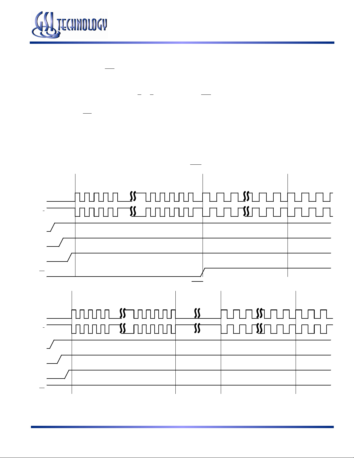
GS8662R08/09/18/36E-333/300/250/200/167
KHDX
DVKH
CHQZ
CQHQXCQHQVCHCQV
CHQV
CHQXCHQX1
KHnKH
KLKHKLKH
KHKLKHKL
KHKHKHKH
Read A Cont Read A NOP Write B Cont Write B Read C
K
KHAX
K
KHIX
AVKH
IVKH
A B C
Address
KHIX
IVKH
LD
R/W
KHKLKHKL
BWx
KHnKH
KLKHKLKH
KHKHKHKH
C
C
A A+1 A+2 A+3 B B+1 B+2 B+3
DQ
CHCQX
CHCQV
CHCQX
CQ
CQ
C and C Controlled Read First Timing Diagram
Rev: 1.01 9/2005 22/37 © 2005, GSI Technology
Specifications cited are subject to change without notice. For latest documentation see http://www.gsitechnology.com.
Page 23

Preliminary
GS8662R08/09/18/36E-333/300/250/200/167
KHDX
KHIX
IVKH
B B+1 B+2 B+3
KH#KH
KLKHKLKH
KHKLKHKL
KHKHKHKH
Read A Cont Read A NOP Write B Cont Write B Read C
KHAX
AVKH
KHIX
IVKH
A B C
KHIX
IVKH
KLKHKLKH
KHKLKHKL
KHKHKHKH
DVKH
KHQZ
KHQV
KHQX
KH#KH
A A+1 A+2 A+3 B B+1 B+2 B+3
KHQX1
CHCQV
CHCQX
CQHQXCQHQVCHCQV
CHCQX
K
K
Address
LD
R/W
BWx
C
C
DQ
CQ
CQ
K and K Controlled Read First Timing Diagram
Rev: 1.01 9/2005 23/37 © 2005, GSI Technology
Specifications cited are subject to change without notice. For latest documentation see http://www.gsitechnology.com.
Page 24

Preliminary
GS8662R08/09/18/36E-333/300/250/200/167
CHQZ
CHQX
CHQVCHQX1
CQHQX
CQHQVCHCQV
KHnKH
KLKHKLKH
KHIX
KHKLKHKL
KHKHKHKH
KHAX
Write A Cont Write A Read B Cont Read B NOP Write C Cont Write C
K
K
KHIX
AVKH
IVKH
A B C
Address
IVKH
KHIX
LD
R/W
KHKLKHKL
IVKH
A A+1 A+2 A+3 C C+1 C+2
BWx
KHnKH
KLKHKLKH
KHDX
KHKHKHKH
C
DVKH
A A+1 A+2 A+3 B B+1 B+2 B+3 C C+1
C
DQ
CHCQX
CQ
CQ
C and C Controlled Write First Timing Diagram
Rev: 1.01 9/2005 24/37 © 2005, GSI Technology
Specifications cited are subject to change without notice. For latest documentation see http://www.gsitechnology.com.
Page 25

Preliminary
GS8662R08/09/18/36E-333/300/250/200/167
KHQZ
KHQXKHQVKHQX1
CQHQX
CQHQV
KHnKH
CHCQV
KLKHKLKH
KHIX
KHKLKHKL
KHKHKHKH
KHAX
Write A1 Cont Write A Read B Cont Read B NOP Write C Cont Write C
K
K
KHIX
AVKH
IVKH
A B C
Address
IVKH
KHDX
KHIX
IVKH
LD
R/W
A A+1 A+2 A+3 C C+1 C+2
BWx
DVKH
A A+1 A+2 A+3 B B+1 B+2 B+3 C C+1 C+2
CHCQV
CHCQX
DQ
CHCQX
CQ
CQ
K and K Controlled Write First Timing Diagram
Rev: 1.01 9/2005 25/37 © 2005, GSI Technology
Specifications cited are subject to change without notice. For latest documentation see http://www.gsitechnology.com.
Page 26

Preliminary
GS8662R08/09/18/36E-333/300/250/200/167
JTAG Port Operation
Overview
The JTAG Port on this RAM operates in a manner that is compliant with the current IEEE Standard, a serial boundary scan
interface standard (commonly referred to as JTAG). The JTAG Port input interface levels scale with V
drivers are powered by V
Disabling the JTAG Port
It is possible to use this device without utilizing the JTAG port. The port is reset at power-up and will remain inactive unless
clocked. TCK, TDI, and TMS are designed with internal pull-up circuits.To assure normal operation of the RAM with the JTAG
Port unused, TCK, TDI, and TMS may be left floating or tied to either V
DD
.
or VSS. TDO should be left unconnected.
DD
JTAG Pin Descriptions
Pin Pin Name I/O Description
. The JTAG output
DD
TCK Test C l oc k In
TMS Test Mode Select In
TDI Test Data In In
TDO Test Data Out Out
Note:
This device does not have a TRST (TAP Reset) pin. TRST is optional in IEEE 1149.1. The Test-Logic-Reset state is entered while TMS is
held high for five rising edges of TCK. The TAP Controller is also reset automatically at power-up.
Clocks all TAP events. All inputs are captured on the rising edge of TCK and all outputs propagate
from the falling edge of TCK.
The TMS input is sampled on the rising edge of TCK. This is the command input for the TAP
controller state machine. An undriven TMS input will produce the same result as a logic one input
level.
The TDI input is sampled on the rising edge of TCK. This is the input side of the serial registers
placed between TDI and TDO. The register placed between TDI and TDO is determined by the
state of the TAP Controller state machine and the instruction that is currently loaded in the TAP
Instruction Register (refer to the TAP Controller State Diagram). An undriven TDI pin will produce
the same result as a logic one input level.
Output that is active depending on the state of the TAP state machine. Output changes in
response to the falling edge of TCK. This is the output side of the serial registers placed between
TDI and TDO.
JTAG Port Registers
Overview
The various JTAG registers, referred to as Test Access Port or TAP Registers, are selected (one at a time) via the sequences of 1s
and 0s applied to TMS as TCK is strobed. Each of the TAP Registers is a serial shift register that captures serial input data on the
rising edge of TCK and pushes serial data out on the next falling edge of TCK. When a register is selected, it is placed between the
TDI and TDO pins.
Instruction Register
The Instruction Register holds the instructions that are executed by the TAP controller when it is moved into the Run, Test/Idle, or
the various data register states. Instructions are 3 bits long. The Instruction Register can be loaded when it is placed between the
TDI and TDO pins. The Instruction Register is automatically preloaded with the IDCODE instruction at power-up or whenever the
controller is placed in Test-Logic-Reset state.
Bypass Register
The Bypass Register is a single bit register that can be placed between TDI and TDO. It allows serial test data to be passed through
the RAM’s JTAG Port to another device in the scan chain with as little delay as possible.
Rev: 1.01 9/2005 26/37 © 2005, GSI Technology
Specifications cited are subject to change without notice. For latest documentation see http://www.gsitechnology.com.
Page 27

Preliminary
GS8662R08/09/18/36E-333/300/250/200/167
Boundary Scan Register
The Boundary Scan Register is a collection of flip flops that can be preset by the logic level found on the RAM’s input or I/O pins.
The flip flops are then daisy chained together so the levels found can be shifted serially out of the JTAG Port’s TDO pin. The
Boundary Scan Register also includes a number of place holder flip flops (always set to a logic 1). The relationship between the
device pins and the bits in the Boundary Scan Register is described in the Scan Order Table following. The Boundary Scan
Register, under the control of the TAP Controller, is loaded with the contents of the RAMs I/O ring when the controller is in
Capture-DR state and then is placed between the TDI and TDO pins when the controller is moved to Shift-DR state. SAMPLE-Z,
SAMPLE/PRELOAD and EXTEST instructions can be used to activate the Boundary Scan Register.
JTAG TAP Block Diagram
·· ······
Boundary Scan Register
·
·
108
0
Bypass Register
·
1
0
012
Instruction Register
TDI
TDO
ID Code Register
31 30 29 12
····
0
Control Signals
TMS
TCK
Test Access Port (TAP) Controller
Identification (ID) Register
The ID Register is a 32-bit register that is loaded with a device and vendor specific 32-bit code when the controller is put in
Capture-DR state with the IDCODE command loaded in the Instruction Register. The code is loaded from a 32-bit on-chip ROM.
It describes various attributes of the RAM as indicated below. The register is then placed between the TDI and TDO pins when the
controller is moved into Shift-DR state. Bit 0 in the register is the LSB and the first to reach TDO when shifting begins.
Rev: 1.01 9/2005 27/37 © 2005, GSI Technology
Specifications cited are subject to change without notice. For latest documentation see http://www.gsitechnology.com.
Page 28

Preliminary
GS8662R08/09/18/36E-333/300/250/200/167
ID Register Contents
Bit # 31 30 29 28 27 26 25 24 23 22 21 20 19 18 17 16 15 14 13 12 11 10 9 8 7 6 5 4 3 2 1 0
x36 X X X X 0 0 0 0 0 1 0 0 1 0 0 1 0 0 0 0 0 0 0 1 1 0 1 1 0 0 1 1
x18 X X X X 0 0 0 0 0 1 0 0 1 0 0 1 0 0 1 0 0 0 0 1 1 0 1 1 0 0 1 1
x9 X X X X 0 0 0 0 0 1 0 0 1 0 0 1 0 0 1 1 0 0 0 1 1 0 1 1 0 0 1 1
x8 X X X X 0 0 0 0 0 1 0 0 1 0 0 1 0 1 1 1 0 0 0 1 1 0 1 1 0 0 1 1
Tap Controller Instruction Set
Overview
There are two classes of instructions defined in the Standard 1149.1-1990; the standard (Public) instructions, and device specific
(Private) instructions. Some Public instructions are mandatory for 1149.1 compliance. Optional Public instructions must be
implemented in prescribed ways. The TAP on this device may be used to monitor all input and I/O pads, and can be used to load
address, data or control signals into the RAM or to preload the I/O buffers.
When the TAP controller is placed in Capture-IR state the two least significant bits of the instruction register are loaded with 01.
When the controller is moved to the Shift-IR state the Instruction Register is placed between TDI and TDO. In this state the desired
instruction is serially loaded through the TDI input (while the previous contents are shifted out at TDO). For all instructions, the
TAP executes newly loaded instructions only when the controller is moved to Update-IR state. The TAP instruction set for this
device is listed in the following table.
Rev: 1.01 9/2005 28/37 © 2005, GSI Technology
Specifications cited are subject to change without notice. For latest documentation see http://www.gsitechnology.com.
Page 29

Test Logic Reset
1
Preliminary
GS8662R08/09/18/36E-333/300/250/200/167
JTAG Tap Controller State Diagram
0
0
Run Test Idle
111
1
1
Select DR
Capture DR
0
Shift DR
Exit1 DR
Pause DR
Exit2 DR
Update DR
1
Select IR
0
1
0
Capture IR
0
Shift IR
1
0
0
1
1
Exit1 IR
0
Pause IR
1
1
0
0 0
1
Exit2 IR
1
Update IR
0
10
0
0
Instruction Descriptions
BYPASS
When the BYPASS instruction is loaded in the Instruction Register the Bypass Register is placed between TDI and TDO. This
occurs when the TAP controller is moved to the Shift-DR state. This allows the board level scan path to be shortened to facili
tate testing of other devices in the scan path.
SAMPLE/PRELOAD
SAMPLE/PRELOAD is a Standard 1149.1 mandatory public instruction. When the SAMPLE / PRELOAD instruction is
loaded in the Instruction Register, moving the TAP controller into the Capture-DR state loads the data in the RAMs input and
I/O buffers into the Boundary Scan Register. Boundary Scan Register locations are not associated with an input or I/O pin, and
are loaded with the default state identified in the Boundary Scan Chain table at the end of this section of the datasheet. Because
the RAM clock is independent from the TAP Clock (TCK) it is possible for the TAP to attempt to capture the I/O ring contents
while the input buffers are in transition (i.e. in a metastable state). Although allowing the TAP to sample metastable inputs will
not harm the device, repeatable results cannot be expected. RAM input signals must be stabilized for long enough to meet the
TAPs input data capture set-up plus hold time (tTS plus tTH). The RAMs clock inputs need not be paused for any other TAP
operation except capturing the I/O ring contents into the Boundary Scan Register. Moving the controller to Shift-DR state then
places the boundary scan register between the TDI and TDO pins.
-
Rev: 1.01 9/2005 29/37 © 2005, GSI Technology
Specifications cited are subject to change without notice. For latest documentation see http://www.gsitechnology.com.
Page 30

Preliminary
GS8662R08/09/18/36E-333/300/250/200/167
EXTEST
EXTEST is an IEEE 1149.1 mandatory public instruction. It is to be executed whenever the instruction register is loaded with
all logic 0s. The EXTEST command does not block or override the RAM’s input pins; therefore, the RAM’s internal state is
still determined by its input pins.
Typically, the Boundary Scan Register is loaded with the desired pattern of data with the SAMPLE/PRELOAD command.
Then the EXTEST command is used to output the Boundary Scan Register’s contents, in parallel, on the RAM’s data output
drivers on the falling edge of TCK when the controller is in the Update-IR state.
Alternately, the Boundary Scan Register may be loaded in parallel using the EXTEST command. When the EXTEST instruction is selected, the sate of all the RAM’s input and I/O pins, as well as the default values at Scan Register locations not associated with a pin, are transferred in parallel into the Boundary Scan Register on the rising edge of TCK in the Capture-DR
state, the RAM’s output pins drive out the value of the Boundary Scan Register location with which each output pin is associ
ated.
IDCODE
The IDCODE instruction causes the ID ROM to be loaded into the ID register when the controller is in Capture-DR mode and
places the ID register between the TDI and TDO pins in Shift-DR mode. The IDCODE instruction is the default instruction
loaded in at power up and any time the controller is placed in the Test-Logic-Reset state.
-
SAMPLE-Z
If the SAMPLE-Z instruction is loaded in the instruction register, all RAM outputs are forced to an inactive drive state (highZ) and the Boundary Scan Register is connected between TDI and TDO when the TAP controller is moved to the Shift-DR
state.
RFU
These instructions are Reserved for Future Use. In this device they replicate the BYPASS instruction.
JTAG TAP Instruction Set Summary
Instruction Code Description Notes
EXTEST 000 Places the Boundary Scan Register between TDI and TDO. 1
IDCODE 001 Preloads ID Register and places it between TDI and TDO. 1, 2
Captures I/O ring contents. Places the Boundary Scan Register between TDI and
SAMPLE-Z 010
RFU 011 Do not use this instruction; Reserved for Future Use. 1
SAMPLE/
PRELOAD
RFU 101 Do not use this instruction; Reserved for Future Use. 1
RFU 110 Do not use this instruction; Reserved for Future Use. 1
BYPASS 111 Places Bypass Register between TDI and TDO. 1
100
TDO.
Forces all RAM output drivers to High-Z.
Captures I/O ring contents. Places the Boundary Scan Register between TDI and
TDO.
1
1
Notes:
1. Instruction codes expressed in binary, MSB on left, LSB on right.
2. Default instruction automatically loaded at power-up and in test-logic-reset state.
Rev: 1.01 9/2005 30/37 © 2005, GSI Technology
Specifications cited are subject to change without notice. For latest documentation see http://www.gsitechnology.com.
Page 31

Preliminary
GS8662R08/09/18/36E-333/300/250/200/167
JTAG Port Recommended Operating Conditions and DC Characteristics
Parameter Symbol Min. Typ. Max. Unit
Power Supply Voltage
Input High Voltage
Input Low Voltage
Output High Voltage (I
Output Low Voltage (I
= –2 mA) V
OH
= 2 mA) V
OL
V
DDQ
V
IH
V
IL
OH
OL
Note: The input level of SRAM pin is to follow the SRAM DC specification.
JTAG Port AC Test Conditions
Parameter Symbol Min Unit
Input High/Low Level
Input Rise/Fall Time TR/TF 1.0/1.0 ns
Input and Output Timing Reference Level 0.9 V
Notes:
1. Distributed scope and test jig capacitance.
2. Test conditions as shown unless otherwise noted.
V
IH/VIL
1.7 1.8 1.9 V
V
1.3 —
DD
+ 0.3
–0.3 — 0.5 V
1.4 —
V
SS
— 0.4 V
V
DD
1.3/0.5 V
V
V
Rev: 1.01 9/2005 31/37 © 2005, GSI Technology
Specifications cited are subject to change without notice. For latest documentation see http://www.gsitechnology.com.
Page 32

TCK
TDI
TMS
TDO
Parallel SRAM input
Preliminary
GS8662R08/09/18/36E-333/300/250/200/167
JTAG Port Timing Diagram
tTKLtTKLtTKHtTKHtTKCtTKC
tTH
tTS
tTH
tTS
tTKQ
tTH
tTS
JTAG Port AC Electrical Characteristics
Parameter Symbol Min. Max Unit
TCK Cycle Time
TCK High Pulse Width
TCK Low Pulse Width
TMS Input Setup Time
TMS Input Hold Time
TDI Input Setup Time
TDI Input Hold Time
SRAM Input Setup Time
SRAM Input Hold Time
Clock Low to Output Valid
t
CHCH
t
CHCL
t
CLCH
t
MVCH
t
CHMX
t
DVCH
t
CHDX
t
SVCH
t
CHSX
t
CLQV
50 — ns
20 — ns
20 — ns
5 — ns
5 — ns
5 — ns
5 — ns
5 — ns
5 — ns
0 10 ns
Rev: 1.01 9/2005 32/37 © 2005, GSI Technology
Specifications cited are subject to change without notice. For latest documentation see http://www.gsitechnology.com.
Page 33

GS8662R08/09/18/36E-333/300/250/200/167
Package Dimensions—165-Bump FPBGA (Package E)
Preliminary
A1 CORNER
1 2 3 4 5 6 7 8 9 10 11
A
B
C
D
E
F
G
H
J
K
L
M
N
P
R
TOP VIEW
M
Ø0.10
M
Ø0.25
Ø0.40~0.60 (165x)
17±0.05
A
C
C A B
14.0
BOTTOM VIEW
11 10 9 8 7 6 5 4 3 2 1
1.01.0
1.0 1.0
10.0
A1 CORNER
A
B
C
D
E
F
G
H
J
K
L
M
N
P
R
C
0.20
C
SEATING PLANE
0.36~0.46
1.50 MAX.
B
0.20(4x)
15±0.05
Rev: 1.01 9/2005 33/37 © 2005, GSI Technology
Specifications cited are subject to change without notice. For latest documentation see http://www.gsitechnology.com.
Page 34

Ordering Information—GSI SigmaCIO DDR-II SRAM
Preliminary
GS8662R08/09/18/36E-333/300/250/200/167
Org Part Number1 Ty pe Package Speed (MHz)
8M x 8 GS8662R08E-333 SigmaCIO DDR-II B4 SRAM 165-bump BGA 333 C
8M x 8 GS8662R08E-300 SigmaCIO DDR-II B4 SRAM 165-bump BGA 300 C
8M x 8 GS8662R08E-250 SigmaCIO DDR-II B4 SRAM 165-bump BGA 250 C
8M x 8 GS8662R08E-200 SigmaCIO DDR-II B4 SRAM 165-bump BGA 200 C
8M x 8 GS8662R08E-167 SigmaCIO DDR-II B4 SRAM 165-bump BGA 167 C
8M x 8 GS8662R08E-333I SigmaCIO DDR-II B4 SRAM 165-bump BGA 333 I
8M x 8 GS8662R08E-300I SigmaCIO DDR-II B4 SRAM 165-bump BGA 300 I
8M x 8 GS8662R08E-250I SigmaCIO DDR-II B4 SRAM 165-bump BGA 250 I
8M x 8 GS8662R08E-200I SigmaCIO DDR-II B4 SRAM 165-bump BGA 200 I
8M x 8 GS8662R08E-167I SigmaCIO DDR-II B4 SRAM 165-bump BGA 167 I
8M x 9 GS8662R09E-333 SigmaCIO DDR-II B4 SRAM 165-bump BGA 333 C
8M x 9 GS8662R09E-300 SigmaCIO DDR-II B4 SRAM 165-bump BGA 300 C
8M x 9 GS8662R09E-250 SigmaCIO DDR-II B4 SRAM 165-bump BGA 250 C
8M x 9 GS8662R09E-200 SigmaCIO DDR-II B4 SRAM 165-bump BGA 200 C
8M x 9 GS8662R09E-167 SigmaCIO DDR-II B4 SRAM 165-bump BGA 167 C
TA
2
8M x 9 GS8662R09E-333I SigmaCIO DDR-II B4 SRAM 165-bump BGA 333 I
8M x 9 GS8662R09E-300I SigmaCIO DDR-II B4 SRAM 165-bump BGA 300 I
8M x 9 GS8662R09E-250I SigmaCIO DDR-II B4 SRAM 165-bump BGA 250 I
8M x 9 GS8662R09E-200I SigmaCIO DDR-II B4 SRAM 165-bump BGA 200 I
8M x 9 GS8662R09E-167I SigmaCIO DDR-II B4 SRAM 165-bump BGA 167 I
4M x 18 GS8662R18E-333 SigmaCIO DDR-II B4 SRAM 165-bump BGA 333 C
4M x 18 GS8662R18E-300 SigmaCIO DDR-II B4 SRAM 165-bump BGA 300 C
4M x 18 GS8662R18E-250 SigmaCIO DDR-II B4 SRAM 165-bump BGA 250 C
4M x 18 GS8662R18E-200 SigmaCIO DDR-II B4 SRAM 165-bump BGA 200 C
4M x 18 GS8662R18E-167 SigmaCIO DDR-II B4 SRAM 165-bump BGA 167 C
4M x 18 GS8662R18E-333I SigmaCIO DDR-II B4 SRAM 165-bump BGA 333 I
4M x 18 GS8662R18E-300I SigmaCIO DDR-II B4 SRAM 165-bump BGA 300 I
4M x 18 GS8662R18E-250I SigmaCIO DDR-II B4 SRAM 165-bump BGA 250 I
4M x 18 GS8662R18E-200I SigmaCIO DDR-II B4 SRAM 165-bump BGA 200 I
4M x 18 GS8662R18E-167I SigmaCIO DDR-II B4 SRAM 165-bump BGA 167 I
Notes:
1. For Tape and Reel add the character “T” to the end of the part number. Example: GS866x36E-300T.
2. TA = C = Commercial Temperature Range. TA = I = Industrial Temperature Range.
Rev: 1.01 9/2005 34/37 © 2005, GSI Technology
Specifications cited are subject to change without notice. For latest documentation see http://www.gsitechnology.com.
Page 35

Ordering Information—GSI SigmaCIO DDR-II SRAM
Preliminary
GS8662R08/09/18/36E-333/300/250/200/167
Org Part Number1 Type Package Speed (MHz)
2M x 36 GS8662R36E-333 SigmaCIO DDR-II B4 SRAM 165-bump BGA 333 C
2M x 36 GS8662R36E-300 SigmaCIO DDR-II B4 SRAM 165-bump BGA 300 C
2M x 36 GS8662R36E-250 SigmaCIO DDR-II B4 SRAM 165-bump BGA 250 C
2M x 36 GS8662R36E-200 SigmaCIO DDR-II B4 SRAM 165-bump BGA 200 C
2M x 36 GS8662R36E-167 SigmaCIO DDR-II B4 SRAM 165-bump BGA 167 C
2M x 36 GS8662R36E-333I SigmaCIO DDR-II B4 SRAM 165-bump BGA 333 I
2M x 36 GS8662R36E-300I SigmaCIO DDR-II B4 SRAM 165-bump BGA 300 I
2M x 36 GS8662R36E-250I SigmaCIO DDR-II B4 SRAM 165-bump BGA 250 I
2M x 36 GS8662R36E-200I SigmaCIO DDR-II B4 SRAM 165-bump BGA 200 I
2M x 36 GS8662R36E-167I SigmaCIO DDR-II B4 SRAM 165-bump BGA 167 I
8M x 8 GS8662R08GE-333 SigmaCIO DDR-II B4 SRAM RoHS-compliant 165-bump BGA 333 C
8M x 8 GS8662R08GE-300 SigmaCIO DDR-II B4 SRAM RoHS-compliant 165-bump BGA 300 C
8M x 8 GS8662R08GE-250 SigmaCIO DDR-II B4 SRAM RoHS-compliant 165-bump BGA 250 C
8M x 8 GS8662R08GE-200 SigmaCIO DDR-II B4 SRAM RoHS-compliant 165-bump BGA 200 C
8M x 8 GS8662R08GE-167 SigmaCIO DDR-II B4 SRAM RoHS-compliant 165-bump BGA 167 C
TA
2
8M x 8 GS8662R08GE-333I SigmaCIO DDR-II B4 SRAM RoHS-compliant 165-bump BGA 333 I
8M x 8 GS8662R08GE-300I SigmaCIO DDR-II B4 SRAM RoHS-compliant 165-bump BGA 300 I
8M x 8 GS8662R08GE-250I SigmaCIO DDR-II B4 SRAM RoHS-compliant 165-bump BGA 250 I
8M x 8 GS8662R08GE-200I SigmaCIO DDR-II B4 SRAM RoHS-compliant 165-bump BGA 200 I
8M x 8 GS8662R08GE-167I SigmaCIO DDR-II B4 SRAM RoHS-compliant 165-bump BGA 167 I
8M x 9 GS8662R09GE-333 SigmaCIO DDR-II B4 SRAM RoHS-compliant 165-bump BGA 333 C
8M x 9 GS8662R09GE-300 SigmaCIO DDR-II B4 SRAM RoHS-compliant 165-bump BGA 300 C
8M x 9 GS8662R09GE-250 SigmaCIO DDR-II B4 SRAM RoHS-compliant 165-bump BGA 250 C
8M x 9 GS8662R09GE-200 SigmaCIO DDR-II B4 SRAM RoHS-compliant 165-bump BGA 200 C
8M x 9 GS8662R09GE-167 SigmaCIO DDR-II B4 SRAM RoHS-compliant 165-bump BGA 167 C
8M x 9 GS8662R09GE-333I SigmaCIO DDR-II B4 SRAM RoHS-compliant 165-bump BGA 333 I
8M x 9 GS8662R09GE-300I SigmaCIO DDR-II B4 SRAM RoHS-compliant 165-bump BGA 300 I
8M x 9 GS8662R09GE-250I SigmaCIO DDR-II B4 SRAM RoHS-compliant 165-bump BGA 250 I
8M x 9 GS8662R09GE-200I SigmaCIO DDR-II B4 SRAM RoHS-compliant 165-bump BGA 200 I
8M x 9 GS8662R09GE-167I SigmaCIO DDR-II B4 SRAM RoHS-compliant 165-bump BGA 167 I
4M x 18 GS8662R18GE-333 SigmaCIO DDR-II B4 SRAM RoHS-compliant 165-bump BGA 333 C
Notes:
1. For Tape and Reel add the character “T” to the end of the part number. Example: GS866x36E-300T.
2. TA = C = Commercial Temperature Range. TA = I = Industrial Temperature Range.
Rev: 1.01 9/2005 35/37 © 2005, GSI Technology
Specifications cited are subject to change without notice. For latest documentation see http://www.gsitechnology.com.
Page 36

Ordering Information—GSI SigmaCIO DDR-II SRAM
Preliminary
GS8662R08/09/18/36E-333/300/250/200/167
Org Part Number1 Type Package Speed (MHz)
4M x 18 GS8662R18GE-300 SigmaCIO DDR-II B4 SRAM RoHS-compliant 165-bump BGA 300 C
4M x 18 GS8662R18GE-250 SigmaCIO DDR-II B4 SRAM RoHS-compliant 165-bump BGA 250 C
4M x 18 GS8662R18GE-200 SigmaCIO DDR-II B4 SRAM RoHS-compliant 165-bump BGA 200 C
4M x 18 GS8662R18GE-167 SigmaCIO DDR-II B4 SRAM RoHS-compliant 165-bump BGA 167 C
4M x 18 GS8662R18GE-333I SigmaCIO DDR-II B4 SRAM RoHS-compliant 165-bump BGA 333 I
4M x 18 GS8662R18GE-300I SigmaCIO DDR-II B4 SRAM RoHS-compliant 165-bump BGA 300 I
4M x 18 GS8662R18GE-250I SigmaCIO DDR-II B4 SRAM RoHS-compliant 165-bump BGA 250 I
4M x 18 GS8662R18GE-200I SigmaCIO DDR-II B4 SRAM RoHS-compliant 165-bump BGA 200 I
4M x 18 GS8662R18GE-167I SigmaCIO DDR-II B4 SRAM RoHS-compliant 165-bump BGA 167 I
2M x 36 GS8662R36GE-333 SigmaCIO DDR-II B4 SRAM RoHS-compliant 165-bump BGA 333 C
2M x 36 GS8662R36GE-300 SigmaCIO DDR-II B4 SRAM RoHS-compliant 165-bump BGA 300 C
2M x 36 GS8662R36GE-250 SigmaCIO DDR-II B4 SRAM RoHS-compliant 165-bump BGA 250 C
2M x 36 GS8662R36GE-200 SigmaCIO DDR-II B4 SRAM RoHS-compliant 165-bump BGA 200 C
2M x 36 GS8662R36GE-167 SigmaCIO DDR-II B4 SRAM RoHS-compliant 165-bump BGA 167 C
2M x 36 GS8662R36GE-333I SigmaCIO DDR-II B4 SRAM RoHS-compliant 165-bump BGA 333 I
TA
2
2M x 36 GS8662R36GE-300I SigmaCIO DDR-II B4 SRAM RoHS-compliant 165-bump BGA 300 I
2M x 36 GS8662R36GE-250I SigmaCIO DDR-II B4 SRAM RoHS-compliant 165-bump BGA 250 I
2M x 36 GS8662R36GE-200I SigmaCIO DDR-II B4 SRAM RoHS-compliant 165-bump BGA 200 I
2M x 36 GS8662R36GE-167I SigmaCIO DDR-II B4 SRAM RoHS-compliant 165-bump BGA 167 I
Notes:
1. For Tape and Reel add the character “T” to the end of the part number. Example: GS866x36E-300T.
2. TA = C = Commercial Temperature Range. TA = I = Industrial Temperature Range.
Rev: 1.01 9/2005 36/37 © 2005, GSI Technology
Specifications cited are subject to change without notice. For latest documentation see http://www.gsitechnology.com.
Page 37

Revision History
Rev. Code: Old; New
Types of
Changes
Format or
Content
Preliminary
GS8662R08/09/18/36E-333/300/250/200/167
Revisions
GS8662Rxx_r1 Format
GS8662Rxx_r1; GS8662Rxx_r1_01 Content
• Creation of new datasheet
• Added RoHS-compliant information
Rev: 1.01 9/2005 37/37 © 2005, GSI Technology
Specifications cited are subject to change without notice. For latest documentation see http://www.gsitechnology.com.
 Loading...