

Datasheet GS8170DD18C-300I, GS8170DD18C-300, GS8170DD18C-250I, GS8170DD18C-250, GS8170DD36C-333I Datasheet (GSI)
...Page 1
Rev: 1.00e 6/2002 1/31 © 2002, GSI Technology, Inc.
Specifications cited are design targets and are subject to change without notice. For latest documentation contact your GSI representative.
Preliminary
GS8170DD18/36C-333/300/250
18Mb Σ1x2Lp Double Data Rate
SigmaRAM™ SRAM
250 MHz–333 MHz
1.8 V V
DD
1.8 V and 1.5 V I/O
209-Bump BGA
Commercial Temp
Industrial Temp
Features
• Double Data Rate Read and Write mode
• JEDEC-standard SigmaRAM
™
pinout and package
• 1.8 V +150/–100 mV core power supply
• 1.5 V or 1.8 V I/O supply
• Pipelined read operation
• Fully coherent read and write pipelines
• Echo Clock outputs track data output drivers
• ZQ mode pin for user-selectable output drive strength
• 2 user-programmable chip enable inputs for easy depth
expansion
• IEEE 1149.1 JTAG-compatible Boundary Scan
• 209-bump, 14 mm x 22 mm, 1 mm bump pitch BGA package
• Pin-compatible with future 36Mb, 72Mb, and 144Mb devices
SigmaRAM Family Overview
GS8170DD18/36 SigmaRAMs are built in compliance with
the SigmaRAM pinout standard for synchronous SRAMs.
They are 18,874,368-bit (18Mb) SRAMs. These are the first in
a family of wide, very low voltage CMOS I/O SRAMs
designed to operate at the speeds needed to implement
economical high performance networking systems.
GSI's ΣRAMs are offered in a number of configurations that
emulate other synchronous SRAMs, such as Burst RAMs,
NBT, Late Write, or Double Data Rate (DDR) SRAMs. The
logical differences between the protocols employed by these
RAMs hinge mainly on various combinations of address
bursting, output data registering and write cueing. The
ΣRAM
™
family standard allows a user to implement the
interface protocol best suited to the task at hand.
Functional Description
Because SigmaRAMs are synchronous devices, address and
read/write control inputs are captured on the rising edge of the
input clock. Write cycles are internally self-timed and initiated
by the rising edge of the clock input. This feature eliminates
complex off-chip write pulse generation required by
asynchronous SRAMs and simplifies input signal timing. In
DDR mode the device captures Data In on both rising and
falling edges of clock and drives data on both clock edges as
well.
Because the DDR ΣRAM always transfers data in two halves,
A0 is internally set to 0 for the first half of each read or write
transfer, and automatically incremented to 1 for the falling
edge transfer. The address field of a DDR ΣRAM is always one
address pin less than the advertised index depth (e.g., the 1M x
18 has a 512k addressable index).
In Pipeline mode, Single Data Rate (SDR) ΣRAMs incorporate
a rising-edge-triggered output register. In DDR mode, risingand falling-edge-triggered output registers are employed. For
read cycles, a DDR SRAM’s output data is staged at the input
of an edge-triggered output register during the access cycle and
then released to the output drivers at the next rising and
subsequent falling edge of clock.
GS817x18/36/72B ΣRAMs are implemented with GSI's high
performance CMOS technology and are packaged in a 209bump BGA.
- 333
Pipeline mode
tKHKH 3.0 ns
tKHQV 1.6 ns
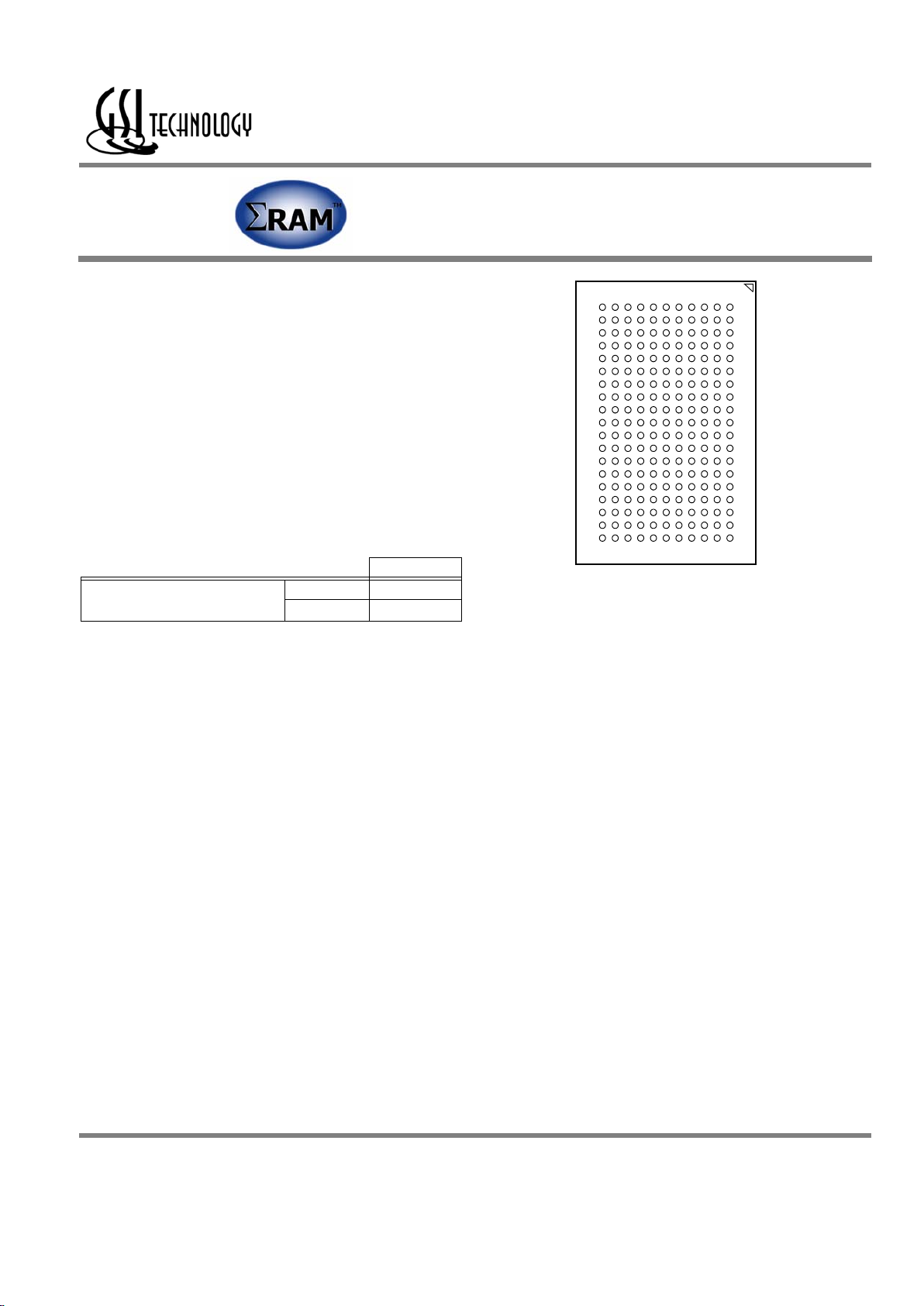
209-Bump, 14 mm x 22 mm BGA
1 mm Bump Pitch, 11 x 19 Bump Array
Bottom View
Page 2
Rev: 1.00e 6/2002 2/31 © 2002, GSI Technology, Inc.
Specifications cited are design targets and are subject to change without notice. For latest documentation contact your GSI representative.
Preliminary
GS8170DD18/36C-333/300/250
8170DD36 512K x 36 Pinout
512K x 36 Common I/O—Top View
1234567891011
A NC NC A E2 A
ADV A E3 A DQb DQb
B NC NC
MCL
NC A W
A
MCL
NC DQb DQb
C NC NC NC MCL NC
(144M)
E1
NC NC MCL DQb DQb
D NC NC V
SS
NC NC MCL NC NC V
SS
DQb DQb
E NC DQc V
DDQ
V
DDI
V
DD
V
DD
V
DD
V
DDI
V
DDQ
NC DQb
F DQc DQc V
SS
V
SS
V
SS
ZQ V
SS
V
SS
V
SS
NC NC
G DQc DQc V
DDQ
V
DDQ
V
DD
EP2 V
DD
V
DDQ
V
DDQ
NC NC
H DQc DQc V
SS
V
SS
V
SS
EP3 V
SS
V
SS
V
SS
NC NC
J DQc DQc V
DDQ
V
DDQ
V
DD
MCH V
DD
V
DDQ
V
DDQ
NC NC
K CQ2 CQ2
CK NC V
SS
MCL V
SS
NC NC CQ1 CQ1
L NC NC V
DDQ
V
DDQ
V
DD
MCL V
DD
V
DDQ
V
DDQ
DQa DQa
M NC NC V
SS
V
SS
V
SS
MCH V
SS
V
SS
V
SS
DQa DQa
N NC NC V
DDQ
V
DDQ
V
DD
MCH V
DD
V
DDQ
V
DDQ
DQa DQa
P NC NC V
SS
V
SS
V
SS
MCL V
SS
V
SS
V
SS
DQa DQa
R DQd NC V
DDQ
V
DDI
V
DD
V
DD
V
DD
V
DDI
V
DDQ
DQa NC
T DQd DQd V
SS
NC NC MCL NC NC V
SS
NC NC
U DQd DQd NC A NC (72M) A NC (36M) A NC NC NC
VDQdDQdAAAA1AAANC NC
WDQdDQdTMSTDI A MCL A TDO TCK NC NC
• 2001.03
11 x 19 Bump BGA—14 x 22 mm2 Body—1 mm Bump Pitch
Page 3
Rev: 1.00e 6/2002 3/31 © 2002, GSI Technology, Inc.
Specifications cited are design targets and are subject to change without notice. For latest documentation contact your GSI representative.
Preliminary
GS8170DD18/36C-333/300/250
8170DD18 1M x 18 Pinout
1M x 18 Common I/O—Top View
1234567891011
A NC NC A E2 A ADV A E3 A NC NC
B NC NC
MCL
NC A W
A NC NC NC NC
C NC NC NC NC NC
(144M)
E1
A NC MCL NC NC
D NC NC V
SS
NC NC MCL NC NC V
SS
NC NC
E NC DQb V
DDQ
V
DDI
V
DD
V
DD
V
DD
V
DDI
V
DDQ
NC NC
F DQb DQb V
SS
V
SS
V
SS
ZQ V
SS
V
SS
V
SS
NC NC
G DQb DQb V
DDQ
V
DDQ
V
DD
EP2 V
DD
V
DDQ
V
DDQ
NC NC
H DQb DQb V
SS
V
SS
V
SS
EP3 V
SS
V
SS
V
SS
NC NC
J DQb DQb V
DDQ
V
DDQ
V
DD
MCH V
DD
V
DDQ
V
DDQ
NC NC
K CQ2 CQ2
CK NC V
SS
MCL V
SS
NC NC CQ1 CQ1
L NC NC V
DDQ
V
DDQ
V
DD
MCL V
DD
V
DDQ
V
DDQ
DQa DQa
M NC NC V
SS
V
SS
V
SS
MCH V
SS
V
SS
V
SS
DQa DQa
N NC NC V
DDQ
V
DDQ
V
DD
MCH V
DD
V
DDQ
V
DDQ
DQa DQa
P NC NC V
SS
V
SS
V
SS
MCL V
SS
V
SS
V
SS
DQa DQa
R NC NC V
DDQ
V
DDI
V
DD
V
DD
V
DD
V
DDI
V
DDQ
DQa NC
T NC NC V
SS
NC NC MCL NC NC V
SS
NC NC
U NC NC NC A NC
(72M)
A NC
(36M)
A NC NC NC
VNCNCAAAA1AAANC NC
WNCNCTMSTDIA MCL A TDO TCK NC NC
• 2001.03
11 x 19 Bump BGA—14 x 22 mm2 Body—1 mm Bump Pitch
Page 4
Rev: 1.00e 6/2002 4/31 © 2002, GSI Technology, Inc.
Specifications cited are design targets and are subject to change without notice. For latest documentation contact your GSI representative.
Preliminary
GS8170DD18/36C-333/300/250
Pin Description Table
Pin Location Symbol Description Type Comments
A3, A5, A7, A9, B7, U4,
U6, U8, V3, V4, V5, V6,
V7, V8, V9, W5, W7
A Address Input —
C7 A Address Input x18 version only
B5 A Address Input x18 and x36 versions
A6 ADV Advance Input Active High
K3 CK Clock Input Active High
K1, K11 CQ Echo Clock Output Active High
K2, K10 CQ
Echo Clock Output Active Low
E2, F1, F2, G1, G2, H1,
H2, J1, J2, L10, L11,
M10, M11, N10, N11,
P10, P11, R10
DQ Data I/O Input/Output x18 and x36 versions
A10, A11, B10, B11,
C10, C11, D10, D11,
E11, R1, T1, T2, U1, U2,
V1, V2, W1, W2
DQ Data I/O Input/Output x36 version
C6 E1
Chip Enable Input Active Low
A4, A8 E2 & E3 Chip Enable Input Programmable Active High or Low
G6, H6 EP2 & EP3 Chip Enable Program Pin Input —
W9 TCK Test Clock Input Active High
W4 TDI Test Data In Input —
W8 TDO Test Data Out Output —
W3 TMS Test Mode Select Input —
J6, M6, N6 MCH Must Connect High Input Active High (all versions)
B3, C9, D6, K6, L6, P6,
T6, W6
MCL Must Connect Low Input Active Low (all versions)
B8, C4 MCL Must Connect Low Input Active Low (x36 version)
Page 5
Rev: 1.00e 6/2002 5/31 © 2002, GSI Technology, Inc.
Specifications cited are design targets and are subject to change without notice. For latest documentation contact your GSI representative.
Preliminary
GS8170DD18/36C-333/300/250
A1, A2, B1, B2, B4, B9,
C1, C2, C3, C5, C8, D1,
D2, D4, D5, D7, D8,E1,
E10, F10, F11, G10,
G11, H10, H11, J10, J11,
K4, K8, K9, L1, L2, M1,
M2, N1, N2, P1, P2, R2,
R11, T4, T5, T7, T8, T10,
T11, U3, U5, U7, U9,
U10, U11, V10, V11,
W10, W11
NC No Connect — Not connected to die (all versions)
C7 NC No Connect — Not connected to die (x36 version)
A1, A2, B1, B2, B4, B9,
C1, C2, C3, C8, D1, D2,
E1, E10, F10, F11, G10,
G11, H10, H11, J10, J11,
L1, L2, M1, M2, N1, N2,
P1, P2, R2, R11, T10,
T11, U10, U11, V10,
V11, W10, W11
NC No Connect — Not connected to die (x36/x18 versions)
A10, A11, B8, B10, B11,
C4, C10, C11, D10, D11,
E11, R1, T1, T2, U1, U2,
V1, V2, W1, W2
NC No Connect — Not connected to die (x18 version)
B6 W
Write Input Active Low
E5, E6, E7, G5, G7, J5,
J7, L5, L7, N5, N7, R5,
R6, R7
V
DD
Core Power Supply Input 1.8 V Nominal
E3, E4, E8, E9, J3, J4,
J8, J9, L3, L4, L8, L9,
N3, N4, N8, N9, R3, R4,
R8, R9
V
DDQ
Output Driver Power Supply Input 1.8 V or 1.5 V Nominal
E4, E8, R4, R8
V
DDI
Input Buffer Power Supply Input 1.8 V or 1.5 V Nominal
D3, D9, F3, F4, F5, F7,
F8, F9, H3, H4, H5, H7,
H8, H9, K5, K7, M3, M4,
M5, M7, M8, M9, P3, P4,
P5, P7, P8, P9, T3, T9
V
SS
Ground Input —
F6 ZQ Output Impedance Control Input
Low = Low Impedance [High Drive]
High = High Impedance [Low Drive]
Pin Description Table
Pin Location Symbol Description Type Comments
Page 6
Rev: 1.00e 6/2002 6/31 © 2002, GSI Technology, Inc.
Specifications cited are design targets and are subject to change without notice. For latest documentation contact your GSI representative.
Preliminary
GS8170DD18/36C-333/300/250
Background
The central characteristics of ΣRAMs are that they are extremely fast and consume very little power. Because both operating and
interface power is low, ΣRAMs can be implemented in a wide (x36) configuration, providing very high single package bandwidth
(in excess of 20 Gb/s in ordinary pipelined configuration) and very low random access latency (5 ns). The use of very low voltage
circuits in the core and 1.8 V or 1.5 V interface voltages allow the speed, power and density performance of ΣRAMs.
The ΣRAM family of pinouts has been designed to support a number of different common read and write protocols. The following
timing diagrams provide a quick comparison between the late write read and write protocol and the DDR protocol options available
in the context of the ΣRAM standard. This particular datasheet covers the Double Data Rate (DDR) ΣRAM.
The character of the applications for fast synchronous SRAMs in networking systems are extremely diverse. ΣRAMs have been
developed to address the broad variety of applications in the networking market in a manner that can be supported with a unified
development and manufacturing infrastructure. ΣRAMs address each of the bus protocol options commonly found in networking
systems. This allows the ΣRAM to find application in radical shrinks and speed-ups of existing networking chip sets that were
designed for use with older SRAMs, like the NBT, Late Write, or Double Data Rate SRAMs, as well as with new chip sets and
ASIC’s that employ the Echo Clocks and realize the full potential of the ΣRAMs.
All address and control inputs (with the exception of PE2, PE3, ZQ, and the mode pins, L6, M6, and J6) are synchronized to rising
clock edges. Data in is captured on both rising and falling edges of CK. Read and write operations must be initiated with the
Advance/Load
pin (ADV) held low, in order to load the new address. Device activation is accomplished by asserting all three of the
Chip Enable inputs (E1
, E2, and E3). Deassertion of any one of the Enable inputs will deactivate the device. It should be noted
that ONLY deactivation of the RAM via E2 and/or E3 deactivates the Echo Clocks, CQ1–CQ2.
Mode Selection Truth Table Standard
L6 M6 J6 Name Function Analogous to... In This Data Sheet?
000
Σ
1x1Ef
Early Write, Flow through Read Flow through Burst RAM No
001
Σ
1x1Lf
Late Write, Flow through Read Flow through NBT SRAM No
010 RFU n/a
011
Σ
1x2Lp
DDR Double Data Rate SRAM Yes
100
Σ
1x1Ep
Early Write, Pipelined Read Pipelined Burst RAM No
101
Σ
1x1Dp
Double Late Write, Pipelined Read Pipelined NBT SRAM No
110
Σ
1x1Lp
Late Write, Pipelined Read Pipelined Late Write SRAM No
Page 7
Rev: 1.00e 6/2002 7/31 © 2002, GSI Technology, Inc.
Specifications cited are design targets and are subject to change without notice. For latest documentation contact your GSI representative.
Preliminary
GS8170DD18/36C-333/300/250
Read Operations
Double Data Rate Read
In applications where a data rate markedly faster than the RAM’s latency is desired, Double Data Rate reads double the data
transfer rate (read or write bandwidth) achieved in Pipeline mode while keeping the RAM’s clock frequency constant. In Double
Data Rate mode, the RAM multiplexes the results of a read out of the RAM on half the usual number of data pins. The output
register/mux behaves just as if it were in Pipeline mode for the first transfer, but then makes a second transfer in response to the
next falling edge of clock as well. SigmaRAM DDR RAMs burst in linear order only.
Double Data Rate Pipelined Read
QA0 QA1 QC0 QC1 QD0 QD1
CK
Read Deselect
AXX F
Read Read Read
ADV
DEC
/E
1
/W
DQ
Address
CQ
Key
Hi-Z Access
Page 8
Rev: 1.00e 6/2002 8/31 © 2002, GSI Technology, Inc.
Specifications cited are design targets and are subject to change without notice. For latest documentation contact your GSI representative.
Preliminary
GS8170DD18/36C-333/300/250
Write Operations
Write operation occurs when the following conditions are satisfied at the rising edge of clock: All three chip enables (E1, E2, and
E3) are active, the write enable input signal (W
) is asserted low, and ADV is asserted low.
Double Data Rate Write
A Double Data Rate Write is a specialized form of Late Write. In Double Data Rate mode, the RAM will capture Data In on both
rising and falling edges of the RAM clock, CK, beginning with the rising edge of clock that follows the capture of the write address
and command.
SigmaRAM Double Data Rate Read and Write
QA0 QA1 DC0 DC1 QD0 QD1
ADV
Read
CQ
E
Deselect
CD
Write ReadRead
CK
Address A
Key
Hi-Z Access
/E
1
/W
DQ
FB
Page 9
Rev: 1.00e 6/2002 9/31 © 2002, GSI Technology, Inc.
Specifications cited are design targets and are subject to change without notice. For latest documentation contact your GSI representative.
Preliminary
GS8170DD18/36C-333/300/250
Special Functions
Burst Cycles
ΣRAMs provide an on-chip burst address generator that can be utilized, if desired, to further simplify burst read or write
implementations. The ADV control pin, when driven high, commands the SRAM to advance the internal address counter and use
the counter generated address to read or write the SRAM. The starting address for the first cycle in a burst cycle series is loaded
into the SRAM by driving the ADV pin low, into Load mode.
SigmaRAM DDR Burst Read with Counter Wrap-around
Counter Wraps
QA2 QA3 QA0 QA1 QA2 QA3 QB0 QB1
ADV
B3A2 B0
CQ
DQ
/E
1
/W
XX
Internal
Address
A2 A0 B2 B1A3
Continue
A1 A3 B 1
B0
CK
XX
Read Continue
Extern al
Address
A2 XX XX
Continue Read
Page 10
Rev: 1.00e 6/2002 10/31 © 2002, GSI Technology, Inc.
Specifications cited are design targets and are subject to change without notice. For latest documentation contact your GSI representative.
Preliminary
GS8170DD18/36C-333/300/250
Burst Order
The burst address counter wraps around to its initial state after four internal addresses (the loaded address and three more) have
been accessed. SigmaRAMs always count in linear burst order.
Linear Burst Order
Notes:
1. The burst counter wraps to initial state on the 3rd rising edge of clock.
2. The DDR SigmaRAM always begins an read or write at A0 = 0. A0 is internally set to 0 at the rising edge of clock and is not
available to the user.
A[1:0] A[1:0]
1st address (Rising Edge CK) 00 10
2nd address (Falling Edge CK) 01 11
3rd address (Rising Edge CK) 10 00
4th address (Falling Edge CK) 11 01
SigmaRAM DDR Burst Write with Counter Wrap-around
ADV
DB2
CQ
DA2 DA3 DA0 DA1 DA2 DA3 DB0 DB1
/E
1
/W
DQ
B2 B3 B1
Counter Wraps
XX
Internal
Address
A2 A3 A0 A1 A2 A3 B 0 B 1
XX B0 XX
Write Continue Continue Write Continue
CK
Extern al
Address
A2 XX
Page 11

Rev: 1.00e 6/2002 11/31 © 2002, GSI Technology, Inc.
Specifications cited are design targets and are subject to change without notice. For latest documentation contact your GSI representative.
Preliminary
GS8170DD18/36C-333/300/250
Echo Clock
ΣRAMs feature Echo Clocks, CQ1,CQ2, CQ
1, and CQ2 that track the performance of the output drivers. The Echo Clocks are
delayed copies of the main RAM clock, CK. Echo Clocks are designed to track changes in output driver delays due to variance in
die temperature and supply voltage. The Echo Clocks are designed to fire with the rest of the data output drivers. SigmaRAMs
provide both in-phase, or true, Echo Clock outputs (CQ1 and CQ2) and inverted Echo Clock outputs (CQ1
and CQ2).
It should be noted that deselection of the RAM via E2 and E3 also deselects the Echo Clock output drivers. The deselection of
Echo Clock drivers is always pipelined to the same degree as output data. Deselection of the RAM via E1
does not deactivate the
Echo Clocks.
Programmable Enables
ΣRAMs feature two user-programmable chip enable inputs, E2 and E3. The sense of the inputs, whether they function as active
low or active high inputs, is determined by the state of the programming inputs, PE2 and PE3. For example, if PE2 is held at V
DD
,
E2 functions as an active high enable. If PE2 is held to V
SS
, E2 functions as an active low chip enable input.
Programmability of E2 and E3 allows four banks of depth expansion to be accomplished with no additional logic. By programming
the enable inputs of four ΣRAMs in binary sequence (00, 01, 10, 11) and driving the enable inputs with two address inputs, four
ΣRAMs can be made to look like one larger RAM to the system.
Example Four Bank Depth Expansion Schematic—Σ1x2Lp
A
CK
E1
E2
E3
W
A1–A
n
CK
W
DQ0–DQ
n
Bank 0
Bank 1 Bank 2
Bank 3
Bank Enable Truth Table
EP2 EP3 E2 E3
Bank 0
V
SS
V
SS
Active Low Active Low
Bank 1 V
SS
V
DD
Active Low Active High
Bank 2
V
DD
V
SS
Active High Active Low
Bank 3
V
DD
V
DD
Active High Active High
E1
A
n – 1
A
n
A1–A
n – 2
A
n – 1
A
n
A1–A
n – 2
A
n – 1
A
n
A1–A
n – 2
A
n – 1
A
n
A1–A
n – 2
DQ
A
CK
E2
E3
W
DQ
A
CK
E2
E3
W
DQ
A
CK
E2
E3
W
DQ
E1
E1
E1
CQ CQ CQ
CQ
CQ
EP2
EP3
0
0
EP2
EP3
1
0 EP2
EP3
0
1
EP2
EP3
1
1
Page 12

Rev: 1.00e 6/2002 12/31 © 2002, GSI Technology, Inc.
Specifications cited are design targets and are subject to change without notice. For latest documentation contact your GSI representative.
Preliminary
GS8170DD18/36C-333/300/250
It should be noted that deselection of the RAM via E2 and E3 also deselects the Echo Clock output drivers. The deselection of
Echo Clock drivers is always pipelined to the same degree as output data. Deselection of the RAM via E1
does not deactivate the
Echo Clocks.
In some applications it may be appropriate to pause between banks; to deselect both RAMs with E1
before resuming read
operations. An E1
deselect at a bank switch will allow at least one clock to be issued from the new bank before the first read cycle
in the bank. Although the following drawing illustrates a E1
read pause upon switching from Bank 1 to Bank 2, a write to Bank 2
would have the same effect, causing the RAM in Bank 2 to issue at least one clock before it is needed.
Echo Clock Control in Two Banks of SigmaRAM Double Data Rate RAMs
QA0 QA1 QC0 QC1
QB0 QB1 QD0 QD1
Note: E1\ does not deselect the Echo Clock Outputs. Echo Clock outputs are synchronously deselected by E2 or E3 being sampled false.
CQ1 + CQ2
Read Read
DQ
Bank 2
CQ
Bank 2
CQ
Bank 1
Read
DQ
Bank 1
Address A B
ADV
Read Read
F
/E2 Bank 1
E2 Bank 2
CDE
CK
Page 13

Rev: 1.00e 6/2002 13/31 © 2002, GSI Technology, Inc.
Specifications cited are design targets and are subject to change without notice. For latest documentation contact your GSI representative.
Preliminary
GS8170DD18/36C-333/300/250
FLXDrive™ Output Driver Impedance Control
The ZQ pin allows selection between ΣRAM nominal drive strength (ZQ floating or low) for multi-drop bus applications and low
drive strength (ZQ high) point-to-point applications. See ”Output Driver Characteristics” on page 42 for details.
SigmaRAM DDR Bank Switch with E1 Deselect
QA0 QA1
QC0 QC1 QD0 QD1
Note: E1\ does not deselect the Echo Clock Outputs. Echo Clock outputs are synchronously deselected by E2 or E3 being sampled false.
F
/E2 Bank 1
E2 Bank 2
DQ
Bank 1
/E
1
C
ADV
Read
D
Read
DQ
Bank 2
CQ
Bank 1
CQ1 + CQ2
Read
CQ
Bank 2
CK
E
Read No Op
Address A XX
Page 14

Rev: 1.00e 6/2002 14/31 © 2002, GSI Technology, Inc.
Specifications cited are design targets and are subject to change without notice. For latest documentation contact your GSI representative.
Preliminary
GS8170DD18/36C-333/300/250
Late Write, Pipelined Read Truth Table
CK
E1
(tn)E(tn)
ADV
(tn)W(tn)
Previous
Operation
Current Operation
DQ/CQ
(tn)
DQ/CQ
(t
n+½
)
DQ/CQ
(t
n+1
)
DQ/CQ
(t
n+1½
)
0→1 X F 0 X X Bank Deselect *** Hi-Z
0
→
1 X X 1 X Bank Deselect Bank Deselect (Continue) Hi-Z Hi-Z
0
→
1 1 T 0 X X Deselect *** Hi-Z/CQ
0
→
1 X X 1 X Deselect Deselect (Continue) Hi-Z/CQ Hi-Z/CQ
0
→
10 T 0 0 X
Write
Loads new address
*** D1/CQ D2/CQ
0
→
1X X 1 X Write
Write Continue
Increments address by 2
Dn-2/CQ Dn-1/CQ Dn/CQ Dn+1/CQ
0
→
10 T 0 1 X
Read
Loads new address
*** Q1/CQ Q2/CQ
0
→
1 X X 1 X Read
Read Continue
Increments address by 2
Qn-2/CQ Qn-2/CQ Qn/CQ Qn+1/CQ
Notes:
1. If E2 = EP2 and E3 = EP3 then E = “T” else E = “F”.
2. “1” = input “high”; “0” = input “low”; “X” = input “don’t care”; “T” = input “true”; “F” = input “false”.
3. “***” indicates that the DQ input requirement / output state and CQ output state are determined by the previous operation.
4. DQs are tri-stated in response to Bank Deselect, Chip Deselect, and Write commands, one full cycle after the command is
sampled.
5. CQs are tri-stated in response to Bank Deselect commands only, one full cycle after the command is sampled.
6. One (1) Continue operation may be initiated after a Read or Write operation is initiated to burst transfer a total of four (4) distinct pieces of data per single external address input. If a second (2nd) Continue operation is initiated, the internal address
wraps back to the initial external (base) address.
Page 15

Rev: 1.00e 6/2002 15/31 © 2002, GSI Technology, Inc.
Specifications cited are design targets and are subject to change without notice. For latest documentation contact your GSI representative.
Preliminary
GS8170DD18/36C-333/300/250
Common I/O State Diagram
Notes:
1. The notation “X,X,X,X” controlling the state transitions above indicate the states of inputs E1
, E, ADV, and W respectively.
2. If (E2 = EP2 and E3 = EP3) then E = “T” else E = “F”.
3. “1” = input “high”; “0” = input “low”; “X” = input “don’t care”; “T” = input “true”; “F” = input “false”.
Deselect
Bank
Deselect
Read
Read
Write
Write
Continue
X,F,0,X or X,X,1,X
Continue
X,F,0,X
1,T,0,X
X,F,0,X
1,T,0,X
1,T,0,X
X,F,0,X
1,T,0,X
1,T,0,X or X,X,1,X
0,T,0,00,T,0,1
0,T,0,00,T,0,1
X,F,0,X
X,F,0,X
0,T,0,0
0,T,0,1 X,X,1,X X,X,1,X
0,T,0,0
0,T,0,1
1,T,0,X
0,T,0,0
0,T,0,1
X,X,1,X X,X,1,X
0,T,0,1 0,T,0,0
Clock (CK)
Command
Current State Next State
ƒƒƒƒ
Current State & Next State Definition for Read/Write Control State Diagram
Current State (n)
Next State (n + 1)
Transition
ƒ
Input Command Code
Key
nn+1n+2n+3
Page 16

Rev: 1.00e 6/2002 16/31 © 2002, GSI Technology, Inc.
Specifications cited are design targets and are subject to change without notice. For latest documentation contact your GSI representative.
Preliminary
GS8170DD18/36C-333/300/250
Note:
Permanent damage to the device may occur if the Absolute Maximum Ratings are exceeded. Operation should be restricted to
Recommended Operating Conditions. Exposure to conditions exceeding the Recommended Operating Conditions, for an extended
period of time, may affect reliability of this component.
Recommended Operating Conditions
Absolute Maximum Ratings
(All voltages reference to V
SS
)
Symbol Description Value Unit
V
DD
Voltage on VDD Pins
–0.5 to 2.5 V
V
DDI
Voltage in V
DDI
Pins
–0.5 to 2.5 V
V
DDQ
Voltage in V
DDQ
Pins –0.5 to V
DD
V
V
I/O
Voltage on I/O Pins
–0.5 to V
DDQ
+0.5 (≤ 2.5 V max.)
V
V
IN
Voltage on Other Input Pins
–0.5 to V
DDI
+0.5 (≤ 2.5 V max.)
V
I
IN
Input Current on Any Pin +/–100 mA dc
I
OUT
Output Current on Any I/O Pin +/–100 mA dc
T
J
Maximum Junction Temperature 125
o
C
T
STG
Storage Temperature –55 to 125
º
C
Power Supplies
Parameter Symbol Min. Typ. Max. Unit Notes
Supply Voltage
V
DD
1.7 1.8 1.95 V
1.8 V Input Supply Voltage
V
DDI
1.7 1.8
V
DD
V1
1.8 V I/O Supply Voltage
V
DDQ
1.7 1.8
V
DD
V1
1.5 V Input Supply Voltage
V
DDI
1.4 1.5 1.6 V V 1
1.5 V I/O Supply Voltage
V
DDQ
1.4 1.5 1.6 V V 1
Ambient Temperature
(Commercial Range Versions)
T
A
02570°C2
Ambient Temperature
(Industrial Range Versions)
T
A
–40 25 85 °C2
Notes:
1. Unless otherwise noted, all performance specifications quoted are evaluated for worst case at both 1.4 V ≤ V
DDQ
≤ 1.6V (i.e., 1.5 V I/O)
and 1.7 V ≤ V
DDQ
≤ 1.95 V (i.e., 1.8 V I/O) and quoted at whichever condition is worst case.
2. Most speed grades and configurations of this device are offered in both Commercial and Industrial Temperature ranges. The part number
of Industrial Temperature Range versions end the character “I”. Unless otherwise noted, all performance specifications quoted are evaluated for worst case in the temperature range marked on the device.
Page 17

Rev: 1.00e 6/2002 17/31 © 2002, GSI Technology, Inc.
Specifications cited are design targets and are subject to change without notice. For latest documentation contact your GSI representative.
Preliminary
GS8170DD18/36C-333/300/250
Note: This parameter is sample tested.
Notes:
1. Junction temperature is a function of SRAM power dissipation, package thermal resistance, mounting board temperature, ambient.
Temperature air flow, board density, and PCB thermal resistance.
2. SCMI G-38-87
3. Average thermal resistance between die and top surface, MIL SPEC-883, Method 1012.1
CMOS I/O DC Input Characteristics
Parameter Symbol Min. Typ. Max. Unit Notes
CMOS Input High Voltage
V
IH
0.65 * V
DDI
—
V
DDI
+ 0.3
V1
CMOS I/O Input High Voltage
V
IH
0.65 * V
DDI
—
V
DDI
+ 0.3
V1
CMOS Input Low Voltage
V
IL
–0.3 —
0.35 * V
DDI
V1
Note: For devices supplied with CMOS input buffers. Compatible with both 1.8 V and 1.5 V I/O drivers.
Capacitance
(TA = 25oC, f = 1 MHZ, V
DD
= 1.8 V)
Parameter Symbol Test conditions Typ. Max. Unit
Input Capacitance
C
IN
V
IN
= 0 V
45pF
Output Capacitance
C
OUT
V
OUT
= 0 V
67pF
Package Thermal Characteristics
Rating Layer Board Symbol Max Unit Notes
Junction to Ambient (at 200 lfm) single
R
ΘJA
TBD °C/W 1,2
Junction to Ambient (at 200 lfm) four
R
ΘJA
TBD °C/W 1,2
Junction to Case (TOP) n/a
R
ΘJC
TBD °C/W 3
20% tKC
V
SS
– 1.0 V
50%
V
SS
V
IH
Undershoot Measurement and Timing Overshoot Measurement and Timing
20% tKC
V
DD
+ 1.0 V
50%
V
DD
V
IL
Page 18

Rev: 1.00e 6/2002 18/31 © 2002, GSI Technology, Inc.
Specifications cited are design targets and are subject to change without notice. For latest documentation contact your GSI representative.
Preliminary
GS8170DD18/36C-333/300/250
AC Test Load Diagram
AC Test Conditions
Parameter Conditions
Input high level
V
DDQ
Input low level 0 V
Max. input slew rate 2 V/ns
Input reference level
V
DDI
/2
Output reference level
V
DDQ
/2
Input and Output Leakage Characteristics
Parameter Symbol Test Conditions Min. Max Notes
Input Leakage Current
(except mode pins)
I
IL
V
IN
= 0 to V
DD
–2 uA 2 uA —
Mode and ZQ, MCH, MCL, EP1, EP2
Pin Input Current
I
INM
V
DD ≥
V
IN
≥
VIL
0 V
≤ V
IN
≤ V
IL
–2 uA
–50 uA
50 uA
2 uA
—
Output Leakage Current
I
OL
Output Disable,
V
OUT
= 0 to V
DDQ
–2 uA 2 uA —
Selectable Impedance Output Driver DC Electrical Characteristics
Parameter Symbol Test Conditions Min. Max Notes
Low Drive Output High Voltage
V
OHL
I
OHL
= –4 mA V
DDQ
– 0.4 V
—1
Low Drive Output Low Voltage
V
OLL
I
OLL
= 4 mA
— 0.4 V 1
High Drive Output High Voltage
V
OHH
I
OHH
= –8 mA V
DDQ
– 0.4 V
—2
High Drive Output Low Voltage
V
OLH
I
OLH
= 8 mA
— 0.4 V 2
Notes:
1. ZQ = 1; High Impedance output driver setting
2. ZQ = 0; Low Impedance output driver setting
DQ
VT = V
DDQ
/2
50Ω
ZQ = High (CMOS I/O)
Page 19

Rev: 1.00e 6/2002 19/31 © 2002, GSI Technology, Inc.
Specifications cited are design targets and are subject to change without notice. For latest documentation contact your GSI representative.
Preliminary
GS8170DD18/36C-333/300/250
Operating Currents
Parameter Symbol
-333 -300 -250
Test Conditions
0°C to
70°C
–40°C to
+85°C
0°C to
70°C
–40°C to
+85°C
0°C to
70°C
–40°C to
+85°C
Operating
Current
x36
I
DDP
Pipeline
345 mA 355 mA 320 mA 330 mA 275 mA 285 mA
E1
≤ V
IL
Max.
tKHKH ≥ tKHKH Min.
All other inputs
V
IL
≥ V
IN
≥ V
IH
x18
I
DDP
Pipeline
245 mA 255 mA 225 mA 235 mA 200 mA 210 mA
Chip Disable
Current
x36
I
SB1
Pipeline
75 mA 85 mA 70 mA 80 mA 65 mA 75 mA
E1
≥ V
IH
Min. or
tKHKH ≥ tKHKH Min.
All other inputs
V
IL
≥ V
IN
≥ V
IH
x18
I
SB1
Pipeline
70 mA 80 mA 65 mA 75 mA 60 mA 70 mA
Bank Deselect
Current
x36
I
SB2
Pipeline
75 mA 85 mA 70 mA 80 mA 65 mA 75 mA
E2 or E3 False
tKHKH ≥ tKHKH Min.
All other inputs
V
IL
≥ V
IN
≥ V
IH
x18
I
SB2
Pipeline
70 mA 80 mA 65 mA 75 mA 60 mA 70 mA
CMOS
Deselect
Current
I
DD3
45 mA 55 mA 45 mA 55 mA 45 mA 55 mA
Device Deselected
All inputs
V
SS
+ 0.10 V
≥ VIN ≥
V
DD
– 0.10 V
Page 20

Rev: 1.00e 6/2002 20/31 © 2002, GSI Technology, Inc.
Specifications cited are design targets and are subject to change without notice. For latest documentation contact your GSI representative.
Preliminary
GS8170DD18/36C-333/300/250
AC Electrical Characteristics
Parameter Symbol
-333 -300 -250
Unit Notes
Min Max Min Max Min Max
Clock Cycle Time tKHKH 3.0 — 3.3 — 4.0 — ns —
Clock High Time tKHKL 1.2 — 1.3 — 1.5 — ns —
Clock Low Time tKLKH 1.2 — 1.3 — 1.5 — ns —
Clock High to Echo Clock Low-Z tKHCX1 0.5 — 0.5 — 0.5 — ns 2
Clock High to Echo Clock High tKHCH 0.5 1.5 0.5 1.7 0.5 2.0 ns —
Echo Clock High Time tCHCL tKHKL +/- 100 ps tKHKL +/- 120 ps ns 2
Clock Low to Echo Clock Low tKLCL 0.5 1.5 0.5 1.7 0.5 2.0 ns
Echo Clock Low Time tCLCH tKLKH +/- 100 ps tKHKL +/- 120 ps ns 2
Clock High to Echo Clock High-Z tKHCZ 0.5 1.5 0.5 1.7 0.5 2.0 ns 1, 2
Clock High to Output in Low-Z tKHQX1 0.5 — 0.5 — 0.5 — ns 1
Clock High to Output Valid tKHQV 1.6 1.8 2.1 ns —
Clock Low to Output Invalid tKLQX 1.6 1.8 2.1 ns —
Clock Low to Output Valid tKLQV 0.5 — 0.5 — 0.5 — ns —
Clock High to Output Invalid tKHQX 0.5 — 0.5 — 0.5 — ns —
Clock High to Output in High-Z tKHQZ 0.5 1.6 0.5 1.8 0.5 2.1 ns 1
Echo Clock High to Output Valid tCHQV — 0.2 — 0.2 — 0.25 ns 2
Echo Clock Low to Output Invalid tCLQX –0.2 — –0.2 — –0.25 — ns 2
Echo Clock Low to Output Valid tCLQV — 0.2 — 0.2 — 0.25 ns 2
Echo Clock High to Output Invalid tCHQX -0.2 — -0.2 — -0.25 — ns 2
Address Valid to Clock High tAVKH 0.6 — 0.7 — 0.8 — ns —
Clock High to Address Don’t Care tKHAX 0.4 — 0.4 — 0.5 — ns —
Enable Valid to Clock High tEVKH 0.6 — 0.7 — 0.8 — ns —
Clock High to Enable Don’t Care tKHEX 0.4 — 0.4 — 0.5 — ns —
Write Valid to Clock High tWVKH 0.6 — 0.7 — 0.8 — ns —
Clock High to Write Don’t Care tKHWX 0.4 — 0.4 — 0.5 — ns —
Clock High to Byte Write Don’t Care tKHBX 0.4 — 0.4 — 0.5 — ns —
Data In Valid to Clock High tDVKH 0.32 — 0.35 — 0.40 — ns —
Clock High to Data In Don’t Care tKHDX 0.27 — 0.30 — 0.35 — ns —
Notes:
1. Measured at 100 mV from steady state. Not 100% tested.
2. Guaranteed by design. Not 100% tested.
3. For any specific temperature and voltage tKHCZ < tKHCX1.
Page 21

Rev: 1.00e 6/2002 21/31 © 2002, GSI Technology, Inc.
Specifications cited are design targets and are subject to change without notice. For latest documentation contact your GSI representative.
Preliminary
GS8170DD18/36C-333/300/250
Data In Valid to Clock Low tDVKL 0.32 — 0.35 — 0.40 — ns
Clock Low to Data In Don’t Care tKLDX 0.27 — 0.30 — 0.35 — ns
ADV Valid to Clock High tadvVKH 0.6 — 0.7 — 0.8 — ns —
Clock High to ADV Don’t Care tKHadvX 0.4 — 0.4 — 0.5 — ns —
Parameter Symbol
-333 -300 -250
Unit Notes
Min Max Min Max Min Max
Notes:
1. Measured at 100 mV from steady state. Not 100% tested.
2. Guaranteed by design. Not 100% tested.
3. For any specific temperature and voltage tKHCZ < tKHCX1.
Page 22

Rev: 1.00e 6/2002 22/31 © 2002, GSI Technology, Inc.
Specifications cited are design targets and are subject to change without notice. For latest documentation contact your GSI representative.
Preliminary
GS8170DD18/36C-333/300/250
Timing Parameter Key—Read Cycle Timing
tKHQX
tKHQZ
tKHQX1
tKHQV
tAVKH
tKHAX
CK
A
DQ (DDR)
tKHKH
tKLKH
tKHKL
CD
E
QB1
CQ
tCHQV tCLQV
tCLQX
tKHCH
tKHCX1
tKHCZ
= CQ High Z
tKLQX
tCLCHtCHCL
tCHQX
tKLQV
QB2
Page 23

Rev: 1.00e 6/2002 23/31 © 2002, GSI Technology, Inc.
Specifications cited are design targets and are subject to change without notice. For latest documentation contact your GSI representative.
Preliminary
GS8170DD18/36C-333/300/250
Timing Parameter Key—Control and Data In Timing
JTAG Port Operation
Overview
The JTAG Port on this RAM operates in a manner that is compliant with IEEE Standard 1149.1-1990, a serial boundary scan
interface standard (commonly referred to as JTAG). The JTAG Port input interface levels scale with V
DDI
. The JTAG output
drivers are powered by V
DDQ
.
Disabling the JTAG Port
It is possible to use this device without utilizing the JTAG port. The port is reset at power-up and will remain inactive unless
clocked. To assure normal operation of the RAM with the JTAG Port unused, TCK, TDI, and TMS may be left floating or tied to
V
DDI
. TDO should be left unconnected.
tKHnX
tnVKH
tAVKH
tKHAX
CK
A
AB
C
E1, E2, E3,
W
, Bn, ADV
tKHDX
tDVKH
DA1 DA2
tKLDX
tDVKL
DDR Write
DQ (Data In)
Note: tnVKH = tEVKH, tWVKH, tBVKH, etc. and tKHnX = tKHEX, tKHWX, tKHBX, etc.
DB1 DB2
Page 24

Rev: 1.00e 6/2002 24/31 © 2002, GSI Technology, Inc.
Specifications cited are design targets and are subject to change without notice. For latest documentation contact your GSI representative.
Preliminary
GS8170DD18/36C-333/300/250
JTAG Port Registers
Overview
The various JTAG registers, refered to as Test Access Port or TAP Registers, are selected (one at a time) via the sequences of 1s
and 0s applied to TMS as TCK is strobed. Each of the TAP registers are serial shift registers that capture serial input data on the
rising edge of TCK and push serial data out on the next falling edge of TCK. When a register is selected, it is placed between the
TDI and TDO pins.
Instruction Register
The Instruction Register holds the instructions that are executed by the TAP controller when it is moved into the Run, Test/Idle, or
the various data register states. Instructions are 3 bits long. The Instruction Register can be loaded when it is placed between the
TDI and TDO pins. The Instruction Register is automatically preloaded with the IDCODE instruction at power-up or whenever the
controller is placed in Test-Logic-Reset state.
Bypass Register
The Bypass Register is a single-bit register that can be placed between TDI and TDO. It allows serial test data to be passed through
the RAM’s JTAG Port to another device in the scan chain with as little delay as possible.
Boundary Scan Register
The Boundary Scan Register is a collection of flip flops that can be preset by the logic level found on the RAM’s input or I/O pins.
The flip flops are then daisy chained together so the levels found can be shifted serially out of the JTAG Port’s TDO pin. The
Boundary Scan Register also includes a number of place holder flip flops (always set to a logic 1). The relationship between the
device pins and the bits in the Boundary Scan Register is described in the Scan Order Table following. The Boundary Scan
Register, under the control of the TAP Controller, is loaded with the contents of the RAMs I/O ring when the controller is in
Capture-DR state and then is placed between the TDI and TDO pins when the controller is moved to Shift-DR state. SAMPLE-Z,
SAMPLE/PRELOAD and EXTEST instructions can be used to activate the Boundary Scan Register.
JTAG Pin Descriptions
Pin Pin Name I/O Description
TCK Test Clock In
Clocks all TAP events. All inputs are captured on the rising edge of TCK and all outputs propagate
from the falling edge of TCK.
TMS Test Mode Select In
The TMS input is sampled on the rising edge of TCK. This is the command input for the TAP
controller state machine. An undriven TMS input will produce the same result as a logic one input
level.
TDI Test Data In In
The TDI input is sampled on the rising edge of TCK. This is the input side of the serial registers
placed between TDI and TDO. The register placed between TDI and TDO is determined by the state
of the TAP Controller state machine and the instruction that is currently loaded in the TAP Instruction
Register (refer to the TAP Controller State Diagram). An undriven TDI pin will produce the same
result as a logic one input level.
TDO Test Data Out Out
Output that is active depending on the state of the TAP state machine. Output changes in response
to the falling edge of TCK. This is the output side of the serial registers placed between TDI and TDO.
Note:
This device does not have a TRST (TAP Reset) pin. TRST is optional in IEEE 1149.1. The Test-Logic-Reset state is entered while TMS is held
high for five rising edges of TCK. The TAP Controller is also reset automaticly at power-up.
Page 25

Rev: 1.00e 6/2002 25/31 © 2002, GSI Technology, Inc.
Specifications cited are design targets and are subject to change without notice. For latest documentation contact your GSI representative.
Preliminary
GS8170DD18/36C-333/300/250
JTAG TAP Block Diagram
Identification (ID) Register
The ID Register is a 32-bit register that is loaded with a device and vendor specific 32-bit code when the controller is put in
Capture-DR state with the IDCODE command loaded in the Instruction Register. The code is loaded from a 32-bit on-chip ROM.
It describes various attributes of the RAM as indicated below. The register is then placed between the TDI and TDO pins when the
controller is moved into Shift-DR state. Bit 0 in the register is the LSB and the first to reach TDO when shifting begins.
Tap Controller Instruction Set
Overview
There are two classes of instructions defined in the Standard 1149.1-1990; standard (Public) instructions, and device specific
(Private) instructions. Some Public instructions are mandatory for 1149.1 compliance. Optional Public instructions must be
implemented in prescribed ways. The TAP on this device may be used to monitor all input and I/O pads. This device will not
perform INTEST but can perform the preload portion of the SAMPLE/PRELOAD command.
ID Register Contents
Die
Revision
Code
Not Used
I/O
Configuration
GSI Technology
JEDEC Vendor
ID Code
Presence Register
Bit # 313029 282726 252423 2221201918 171615 1413121110987654321 0
x36
0000000000000001100000011011001 1
x18
0000000000000001101000011011001 1
Instruction Register
ID Code Register
Boundary Scan Register
012
012
····
31 30 29
012
···
······
n
0
Bypass Register
TDI
TDO
TMS
TCK
Test Access Port (TAP) Controller
Page 26

Rev: 1.00e 6/2002 26/31 © 2002, GSI Technology, Inc.
Specifications cited are design targets and are subject to change without notice. For latest documentation contact your GSI representative.
Preliminary
GS8170DD18/36C-333/300/250
When the TAP controller is placed in Capture-IR state, the two least significant bits of the instruction register are loaded with 01.
When the controller is moved to the Shift-IR state, the Instruction Register is placed between TDI and TDO. In this state the
desired instruction is serially loaded through the TDI input (while the previous contents are shifted out at TDO). For all
instructions, the TAP executes newly loaded instructions only when the controller is moved to Update-IR state. The TAP
instruction set for this device is listed in the following table.
JTAG Tap Controller State Diagram
Instruction Descriptions
BYPASS
When the BYPASS instruction is loaded in the Instruction Register, the Bypass Register is placed between TDI and TDO. This occurs when
the TAP controller is moved to the Shift-DR state. This allows the board level scan path to be shortened to facilitate testing of other devices
in the scan path.
SAMPLE/PRELOAD
SAMPLE/PRELOAD is a Standard 1149.1 mandatory public instruction. When the SAMPLE / PRELOAD instruction is loaded in the Instruction Register, moving the TAP controller into the Capture-DR state loads the data in the RAMs input and I/O buffers into the Boundary Scan
Register. Some Boundary Scan Register locations are not associated with an input or I/O pin, and are loaded with the default state identified
in the BSDL file. Because the RAM clock is independent from the TAP Clock (TCK) it is possible for the TAP to attempt to capture the I/O
ring contents while the input buffers are in transition (i.e. in a metastable state). Although allowing the TAP to sample metastable inputs will
not harm the device, repeatable results cannot be expected. RAM input signals must be stabilized for long enough to meet the TAP’s input
data capture set-up plus hold time (tTS plus tTH ). The RAM’s clock inputs need not be paused for any other TAP operation except capturing
Select DR
Capture DR
Shift DR
Exit1 DR
Pause DR
Exit2 DR
Update DR
Select IR
Capture IR
Shift IR
Exit1 IR
Pause IR
Exit2 IR
Update IR
Test Logic Reset
Run Test Idle
0
0
1
0
1
1
0
0
1
1
1
0
0
1
1
0
0
0
0
1
1
0 0
1
1
0
0
0
1
111
Page 27

Rev: 1.00e 6/2002 27/31 © 2002, GSI Technology, Inc.
Specifications cited are design targets and are subject to change without notice. For latest documentation contact your GSI representative.
Preliminary
GS8170DD18/36C-333/300/250
the I/O ring contents into the Boundary Scan Register. Moving the controller to Shift-DR state then places the Boundary Scan Register
between the TDI and TDO pins. The Update-DR controller state transfers the contents of boundary scan cells into the holding register of
each cell associated with an output pin on the RAM.
EXTEST
EXTEST is an IEEE 1149.1 mandatory public instruction. It is to be executed whenever the instruction register is loaded with all logic 0s. The
EXTEST command does not block or override the RAM’s input pins (except CK); therefore, the RAM’s internal state is still determined by its
input pins.
Typically, the Boundary Scan Register is loaded with the desired pattern of data with the SAMPLE/PRELOAD command. Then the EXTEST
command is used to output the Boundary Scan Register’s contents, in parallel, on the RAM’s data output drivers on the falling edge of TCK
when the controller is in the Update-IR state.
Alternately, the Boundary Scan Register may be loaded in parallel using the EXTEST command. When the EXTEST instruction is selected,
the state of all the RAM’s input and I/O pins, as well as the default values at Scan Register locations not associated with a pin, are sampled
and transferred in parallel into the Boundary Scan Register on the rising edge of TCK in the Capture-DR state. Boundary Scan Register contents may then be shifted serially through the register using the Shift-DR command or the controller can be skipped to the Update-DR command. When the controller is placed in the Update-DR state, a RAM that has a fully compliant EXTEST function drives out the value of the
Boundary Scan Register location associated with which each output pin.
IDCODE
The IDCODE instruction causes the ID ROM to be loaded into the ID register when the controller is in Capture-DR mode and places the ID
register between the TDI and TDO pins in Shift-DR mode. The IDCODE instruction is the default instruction loaded in at power up and any
time the controller is placed in the Test-Logic-Reset state.
SAMPLE-Z/PRELOAD
The SAMPLE-Z instruction operates exactly like SAMPLE/PRELOAD except that loading the SAMPLE-Z instruction forces all the RAM’s
output drivers, except TDO, to an inactive drive state (high-Z).
RFU
These instructions are reserved for future use.
Page 28

Rev: 1.00e 6/2002 28/31 © 2002, GSI Technology, Inc.
Specifications cited are design targets and are subject to change without notice. For latest documentation contact your GSI representative.
Preliminary
GS8170DD18/36C-333/300/250
JTAG TAP Instruction Set Summary
Instruction Code Description Notes
EXTEST 000 Places the Boundary Scan Register between TDI and TDO. 1
IDCODE 001 Preloads ID Register and places it between TDI and TDO. 1, 2
SAMPLE-Z/
PRELOAD
010
Captures I/O ring contents. Places the Boundary Scan Register between TDI and TDO.
Forces all Data and Clock output drivers to High-Z.
1
Private 011 Private instruction. 1
SAMPLE/
PRELOAD
100 Captures I/O ring contents. Places the Boundary Scan Register between TDI and TDO. 1
Private 101 Private instruction. 1
Private 110 Private instruction. 1
BYPASS 111 Places Bypass Register between TDI and TDO. 1
Notes:
1. Instruction codes expressed in binary, MSB on left, LSB on right.
2. Default instruction automatically loaded at power-up and in Test-Logic-Reset state.
JTAG Port Recommended Operating Conditions and DC Characteristics
Parameter Symbol Min. Max. Unit Notes
Test Port Input High Voltage
V
IHT
0.65 * V
DD
VDD+0.3
V1
Test Port Input Low Voltage
V
ILT
–0.3
0.35 * V
DD
V1
TMS, TCK and TDI Input Leakage Current
I
INTH
–2 2 uA 2
TMS, TCK and TDI Input Leakage Current
I
INTL
–50 2 uA 3
TDO Output Leakage Current
I
OLT
–2 2 uA 4
Test Port Output High Voltage
V
OHT
VDD – 100 mV
—V5, 6
Test Port Output Low Voltage
V
OLT
— 100 mV V 7
Notes:
1. Input Under/overshoot voltage must be –1 V < Vi < V
DD
+ 1 V with a pulse width not to exceed 20% tTKC.
2. V
DDI ≥
V
IN
≥
VIL
3. 0 V
≤ V
IN
≤ V
IL
4. Output Disable, V
OUT
= 0 to V
DDI
5. The TDO output driver is served by the V
DDQ
supply.
6. I
OH
= –100 uA
7. I
OL
= +100 uA
Page 29

Rev: 1.00e 6/2002 29/31 © 2002, GSI Technology, Inc.
Specifications cited are design targets and are subject to change without notice. For latest documentation contact your GSI representative.
Preliminary
GS8170DD18/36C-333/300/250
JTAG Port Timing Diagram
JTAG Port AC Electrical Characteristics
Parameter Symbol Min Max Unit
TCK Cycle Time tTKC 50 — ns
TCK Low to TDO Valid tTKQ — 10 ns
TCK High Pulse Width tTKH 20 — ns
TCK Low Pulse Width tTKL 20 — ns
TDI & TMS Set Up Time tTS 5 — ns
TDI & TMS Hold Time tTH 5 — ns
Notes:
1. Include scope and jig capacitance.
2. Test conditions as as shown unless otherwise noted.
JTAG Port AC Test Conditions
Parameter Conditions
Input high level
V
DDI
– 200 mV
Input low level 200 mV
Input slew rate 1 V/ns
Input reference level
V
DDI
/2
Output reference level
V
DDQ
/2
DQ
V
T
= V
DDQ
/2
50Ω
JTAG Port AC Test Load
tTKQ
tTS tTH
tTKH
tTKL
TCK
TMS
TDI
TDO
tTKC
Page 30

Rev: 1.00e 6/2002 30/31 © 2002, GSI Technology, Inc.
Specifications cited are design targets and are subject to change without notice. For latest documentation contact your GSI representative.
Preliminary
GS8170DD18/36C-333/300/250
209 BGA Package Drawing
14 mm x 22 mm Body, 1.0 mm Bump Pitch, 11 x 19 Bump Array
Symbol Min Typ Max Units
A 1.70 mm
A1
0.40 0.50 0.60 mm
∅b 0.50 0.60 0.70 mm
c 0.31 0.36 0.38 mm
D
21.9 22.0 22.1 mm
D1 18.0 (BSC) mm
E 13.9 14.0 14.1 mm
E1
10.0 (BSC) mm
e
1.00 (BSC) mm
aaa
0.15 mm
Rev 1.0
A
A1
C
∅b
e
e
E
E1
D1
D
aaa
Bottom View
Side View
Page 31

Rev: 1.00e 6/2002 31/31 © 2002, GSI Technology, Inc.
Specifications cited are design targets and are subject to change without notice. For latest documentation contact your GSI representative.
Preliminary
GS8170DD18/36C-333/300/250
Ordering Information—GSI SigmaRAM
Org
Part Number
1
Type Package
Speed
(MHz)
T
A
3
512K x 36 GS8170DD36C-333
Σ
1x2Lp DDR ΣRAM
1 mm Pitch, 209-Pin BGA 333 C
512K x 36 GS8170DD36C-300
Σ
1x2Lp DDR ΣRAM
1 mm Pitch, 209-Pin BGA 300 C
512K x 36 GS8170DD36C-250
Σ
1x2Lp DDR ΣRAM
1 mm Pitch, 209-Pin BGA 250 C
512K x 36 GS8170DD36C-333I
Σ
1x2Lp DDR ΣRAM
1 mm Pitch, 209-Pin BGA 333 I
512K x 36 GS8170DD36C-300I
Σ
1x2Lp DDR ΣRAM
1 mm Pitch, 209-Pin BGA 300 I
512K x 36 GS8170DD36C-250I
Σ
1x2Lp DDR ΣRAM
1 mm Pitch, 209-Pin BGA 250 I
1Mx 18 GS8170DD18C-333
Σ
1x2Lp DDR ΣRAM
1 mm Pitch, 209-Pin BGA 333 C
1Mx 18 GS8170DD18C-300
Σ
1x2Lp DDR ΣRAM
1 mm Pitch, 209-Pin BGA 300 C
1Mx 18 GS8170DD18C-250
Σ
1x2Lp DDR ΣRAM
1 mm Pitch, 209-Pin BGA 250 C
1Mx 18 GS8170DD18C-333I
Σ
1x2Lp DDR ΣRAM
1 mm Pitch, 209-Pin BGA 333 I
1Mx 18 GS8170DD18C-300I
Σ
1x2Lp DDR ΣRAM
1 mm Pitch, 209-Pin BGA 300 I
1Mx 18 GS8170DD18C-250I
Σ
1x2Lp DDR ΣRAM
1 mm Pitch, 209-Pin BGA 250 I
Notes:
1. Customers requiring delivery in Tape and Reel should add the character “T” to the end of the part number. Example:
GS817x18C-300T.
2. T
A
= C = Commercial Temperature Range. TA = I = Industrial Temperature Range.
 Loading...