

Page 1
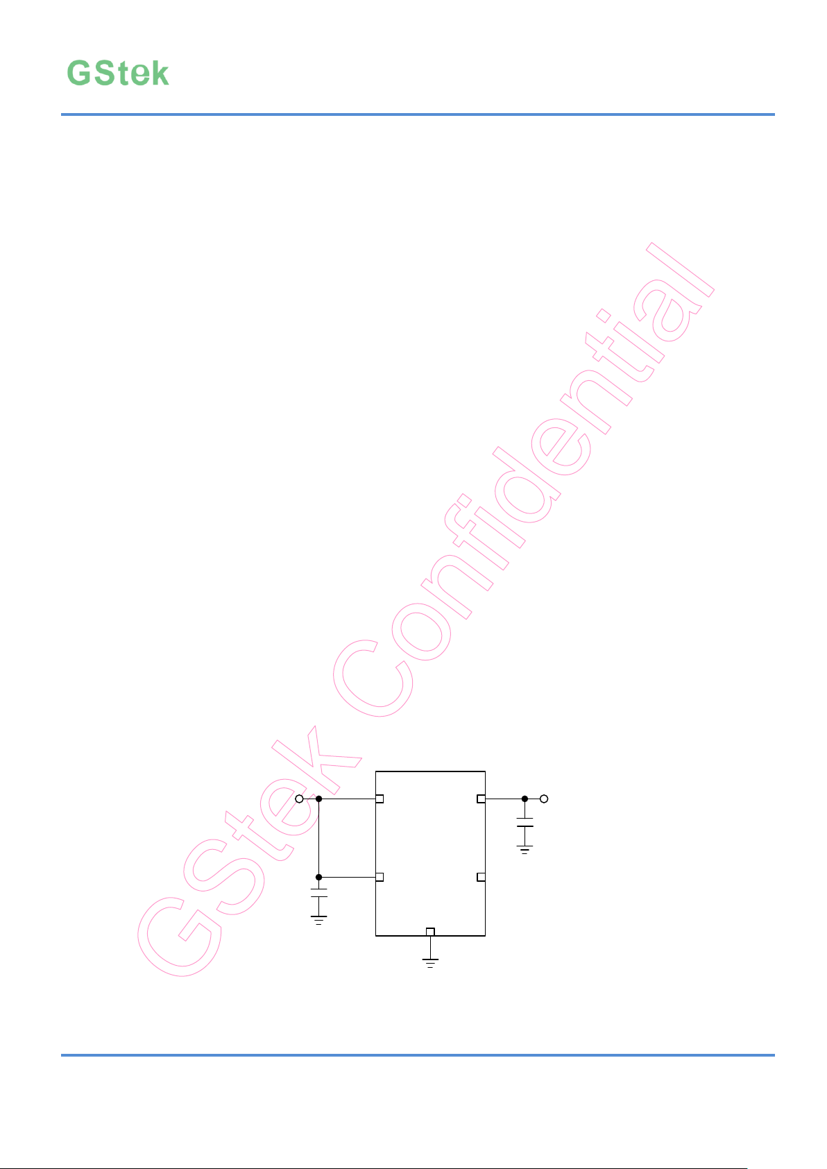
300mA, Fast Transient Response LDO Regulator GS7132
1.8V~5.5V
VDD
EN
1uF
1uF
Vout
NC
GS7132
1
3 4
5
2
This document is GStek's confidential information. Anyone having confidential obligation to GStek shall keep this document confidential. Any unauthorized
disclosure or use beyond authorized purpose will be considered as violation of confidentiality and criminal and civil liability will be asserted.
Features
Optimized for fast transient response
General Description
The GS7132 is a CMOS linear regulator
Low Shutdown Current ~0.1uA (Typ.)
Output Current ~300mA
High Power Supply Rejection Ratio
~70db@1KHz
1.8~5.5V Operation
±2% Initial Voltage Accuracy
Low Temperature Drift Coefficient ~100ppm
Line Regulation ~0.06%/V(Typ.)
Low ESR Capacitor ~1uF ceramic capacitor
uDFN4-1x1、SOT-23-5、SOT-23、
SOT-353(SC-75) 、SOT-89-5、TDFN6-2x2
package
Green Product (RoHS, Lead-Free,
Halogen-Free Compliant)
Applications
Portable communication equipment
optimized for fast transient response. It
guarantees delivery of 300mA output current. The
device is available in fixed output voltage from
1.0V~4.8V and as an adjustable device with a
1.0V reference voltage.
Based on its low quiescent current consumption
and its less than 1uA shutdown mode, the
GS7132 is ideal for battery- powered applications.
The line transient response and load transient
response of the GS7132 are excellent, thus the
device is suitable for the power supply for
handheld communication equipment. The
regulator is stable with small ceramic capacitive
loads (1µF typical).
Notebook Computer
Battery Powered Systems
Typical Application
Figure 1(a) Fix mode of GS7132
Green Solution Technology Co.,LTD.
Rev.:1.72 1 Jan-17
Page 2
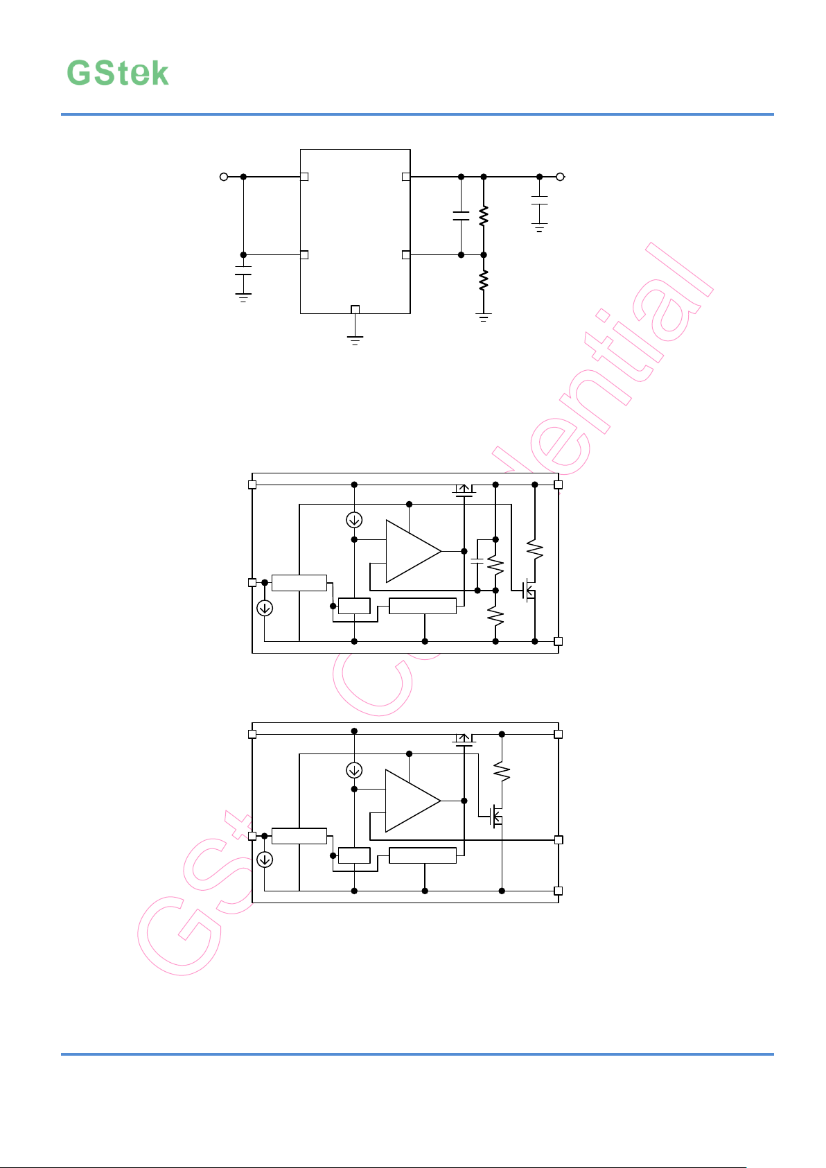
300mA, Fast Transient Response LDO Regulator GS7132
Coption
Coption:10p~100p
1.8V~5.5V
VDD
EN
1uF
1uF
Vout
SET
GS7132
1
3 4
5
2
R2
R1
R1=100K
Vout=(1+R2/R1)*1V
Current Limit
Vref
VDD
EN
GND
VOUT
0.4uA
EN Control
EN
+
-
Current Limit
Vref
EN
+
-
VDD
EN
GND
VOUT
SET
EN Control
0.4uA
Figure 1(b) Adjustable mode of GS7132
Function Block Diagram
Figure 2(a) Functional diagram of Fix mode
Figure 2(b) Functional diagram of Adjustable mode
Figure 2 Function Block Diagram
Green Solution Technology Co.,LTD.
Rev.:1.72 2 Jan-17
Page 3
300mA, Fast Transient Response LDO Regulator GS7132
1
2 3
6 5 4
VDD GND EN
SET / NCVOUT
1 2 3
45
(Top view)
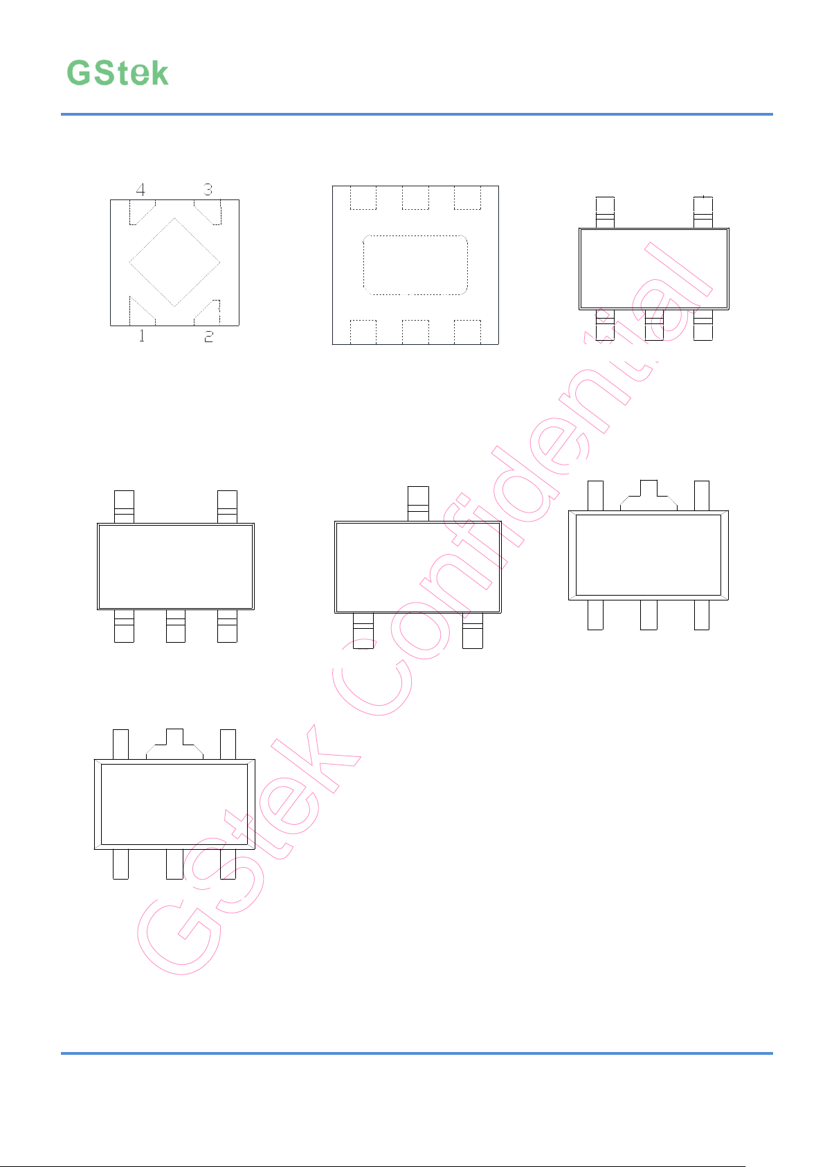
Figure 3a uDFN4-1x1
package
(Top view)
Figure 3b TDFN6-2x2
package
Figure 3c SOT-23-5(ST)/
SOT-353 package
1
2 3
4
5
VDDGND
EN
SET/NC
VOUT
GND
1
2
3
VOUT
VDD/EN
1 2 3
5
4
VOUT GND NC
VDD EN
Figure 3d SOT-23-5(S5) package
Figure 3e MSOT-23 package
Figure 3f SOT-89-5(S1) package
1 2 3
5
4
NC GND EN
VOUT VDD
Figure 3g SOT-89-5(S8) package
VOUT
GND
5. NC
NC
NC
EN
GND
VDD
VOUT
VDD
EN
7.GND
Pin Configuration
The dissipation pad for the uDFN4-1X1 and TDFN6-2x2 packages should be solder-plated in reference mount pattern
and metal masking so as to enhance mounting strength and heat release. If the pad needs to be connected to other
pins, it should be connected to the GND pin.
Green Solution Technology Co.,LTD.
Rev.:1.72 3 Jan-17
Page 4
300mA, Fast Transient Response LDO Regulator GS7132
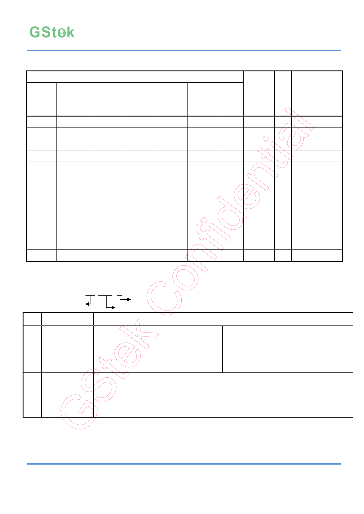
No
Name
I/O
type
Description
uDFN4
-1x1
SOT-23-5
(ST)/
SOT-353
SOT-23-5
(S5)
MSOT-23
SOT-89-5
(S1)
SOT-89-5
(S8)
TDFN6
-2x2
2 2 2 1 2 2 2,7
GND
I/O
Ground pin
4 1 3 3 5 4 3
VDD
I
Input Voltage Pin
1 5 4 2 1 5 4
VOUT
O
Output Voltage Pin
3 3 1 3 4 3 1
EN
I
Enable Pin
4 5
SET
O
Not connected/
Connected to the
center tap of an
external resistor
divider network to
set the output
voltage as V
OUT
=(1+R2/R1)*1V
5
4 5 3 1
5,6
NC
No internal
Connection.
No
Item
Contents
1
Package
UD: uDFN4-1x1
ST: SOT-23-5(ST)
S5: SOT-23-5(S5)
SR: MSOT-23
C5: SOT-353 (SC-75)
D2:TDFN6-2x2
S1: SOT-89-5
S8: SOT-89-5
2
Output Voltage
ADJ: ADJ, 105:1.05V, 1P3: 1.3V, 1P5: 1.5V, 1P8: 1.8V, 185:1.85V, 002: 2.0V, 2P3:
2.3V, 2P5: 2.5V, 2P6: 2.6V, 2P7: 2.7V, 2P8: 2.8V, 2P9: 2.9V, 003: 3.0V, 3P1: 3.1V,3P3:
3.3V,3P5: 3.5V
3
Shipping
R: Tape & Reel
GS7132PP-XXX- R
3. Shipping
2. Output Voltage
1. Package
Pin Descriptions
Ordering Information
Example: GS7132 MSOT-23 2.5V Tape & Reel ordering information is “GS7132SR-2P5-R”
Green Solution Technology Co.,LTD.
Rev.:1.72 4 Jan-17
Page 5
300mA, Fast Transient Response LDO Regulator GS7132
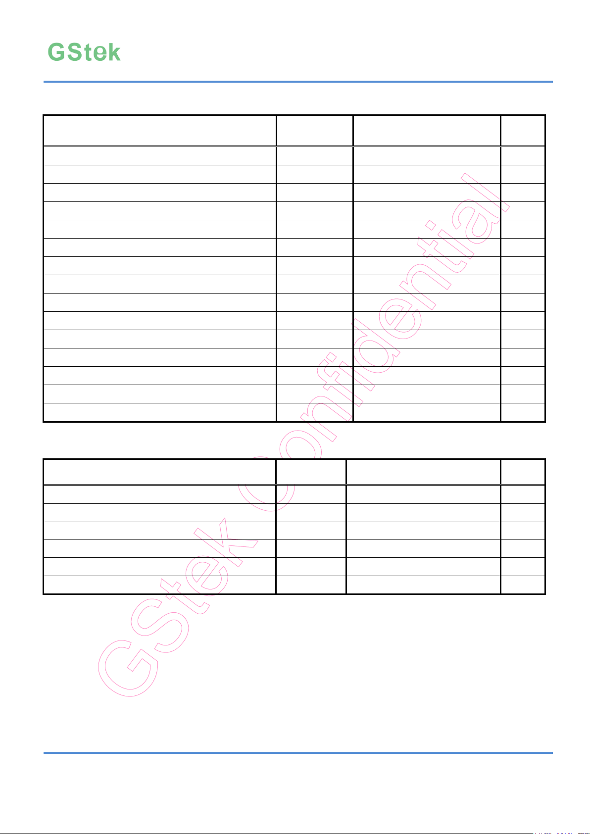
Parameter
Symbol
Limits
Units
VDD to GND
VDD
-0.3 < VDD < 5.5
V
VEN to GND
VEN
-0.3 < VEN< 5.5
V
Output Voltage
V
OUT
-0.3 < V
OUT
< VDD +0.3
V
Output Current
I
OUT
300
mA
Package Power Dissipation at TA≦25°C
P
D_uDFN4-1x1
400
mW
Package Power Dissipation at TA≦25°C
P
D_SOT-23-5
420
mW
Package Power Dissipation at TA ≦25°C
P
D_SOT-353
300
mW
Package Power Dissipation at TA≦25°C
P
D_MSOT-23
380
mW
Package Power Dissipation at TA≦25°C
P
D_SOT-89-5
500
mW
Package Power Dissipation at TA =25°C
P
D_TDFN6-2x2
1087
mW
Junction Temperature
TJ
- 45 ~ 150
°C
Storage Temperature
T
STG
- 65 ~ 150
°C
Lead Temperature (Soldering) 10S
T
LEAD
260
°C
ESD (Human Body Mode) (Note 2)
V
ESD_HBM
2K
V
ESD (Machine Mode) (Note 2)
V
ESD_MM
200
V
Parameter
Symbol
Limits
Units
Thermal Resistance Junction to Ambient
θ
JA_uDFN4-1x1
250
°C/W
Thermal Resistance Junction to Ambient
θ
JA_SOT-23-5
238
°C/W
Thermal Resistance Junction to Ambient
θ
JA_SOT-353
333
°C/W
Thermal Resistance Junction to Ambient
θ
JA_MSOT-23
263
°C/W
Thermal Resistance Junction to Ambient
θ
JA_SOT-89-5
200
°C/W
Thermal Resistance Junction to Ambient
θ
JA_TDFN6-2x2
92
°C/W
Absolute Maximum Rating (Note 1)
Thermal Information (Note 3)
Green Solution Technology Co.,LTD.
Rev.:1.72 5 Jan-17
Page 6
300mA, Fast Transient Response LDO Regulator GS7132
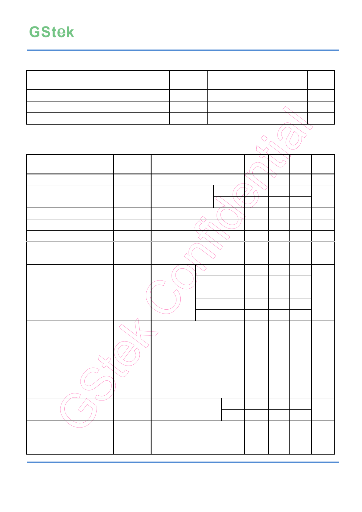
Parameter
Symbol
Limits
Units
VDD to GND
VDD
1.8 to 5.5
V
Junction Temperature
TJ
- 40 ~ 125
°C
Ambient Temperature
TA
-40 ~ 85
°C
Parameter
Symbol
Conditions
Min
Typ
Max
Units
Supply Voltage
VDD
1.8
5.5
V
Supply Current
I
VDD
VDD=3.5V, V
OUT
=2.5V ,Unload
FIX
93
140
uA
ADJ
85
130
Standby Current
I
STBY
VEN=0
0.1
1.0
uA
EN Input Current
IEN
VEN= 5V
0.4 uA
Output Current
I
OUT
300
mA
Output Voltage
V
OUT
I
OUT
=1mA, V
OUT
=1.0V~ 4.8V
-2 +2
%
Dropout Voltage (Note 5)
V
DROP
I
OUT
=300mA
V
OUT
=1.2V
940
1200
mV
V
OUT
=1.8V
580
750
V
OUT
=2.5V
400
510
V
OUT
=2.8V
380
500
V
OUT
=3.3V
330
450
Line Regulation
△V
LNR
VDD= V
OUT
+1V to 5.5V,
I
OUT
=10mA
0.06
0.12
%/V
Load Regulation
△V
LDR
VDD= V
OUT
+1V,
I
OUT
=1mA to 150mA
0.005
0.018
%/mA
Ripple Rejection Rate
PSRR
VDD=MAX{V
OUT
+1.0V, 3V},
Ripple 0.2Vp-p, I
OUT
=10mA,
f=1KHz
70 dB
Limit Current
I
LIM
VDD=3.5V, V
OUT
=2.5V
FIX
450
505
650
mA
ADJ
500
625
750
Short Current
I
SHORT
V
OUT
=0V, VDD=3.5V
90
150
200
mA
EN Input Voltage High
V
ENH
1.2
V
EN Input Voltage Low
V
ENL
0.3
V
Recommend Operating Condition (Note 4)
Electrical Characteristics
(VDD = V
+ 1V, TA =TJ=25°C, C
OUT
VDD=CVOUT
=1uF, I
=1mA, unless otherwise specified)
OUT
Green Solution Technology Co.,LTD.
Rev.:1.72 6 Jan-17
Page 7
300mA, Fast Transient Response LDO Regulator GS7132
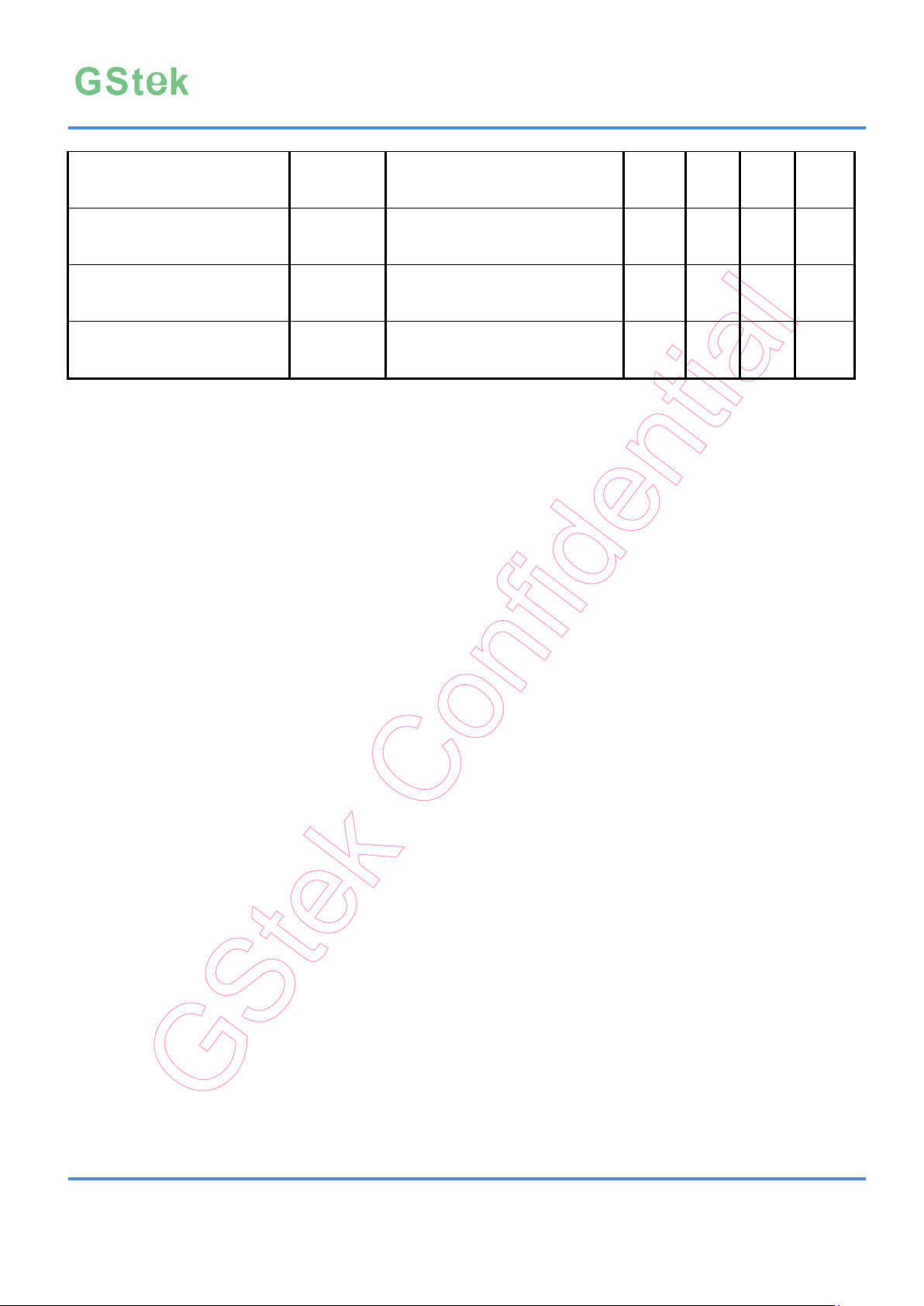
CL Auto-Discharge
Resistance
R
DISCHG
VDD=4.0V, VEN=0V
103
Ω Temperature Drift
△V
OUT
/△TA
I
OUT
=1mA,
TA= -40°C to +85°C
100
ppm/°C
Thermal Shutdown
temperature
T
SHDN
155 °C
Thermal Shutdown
Hysteresis
△T
SHDN
20 °C
Note 1. Stresses listed as the above “Absolute Maximum Ratings” may cause permanent damage to the
device. These are for stress ratings. Functional operation of the device at these or any other
conditions beyond those indicated in the operational sections of the specifications is not implied.
Exposure to absolute maximum rating conditions for extended periods may remain possibility to
affect device reliability.
Note 2. Devices are ESD sensitive. Handling precaution recommended.
Note 3. θ
is measured in the natural convection at TA=25°C on a high effective thermal conductivity test
JA
board (4 Layers, 2S2P) of JEDEC 51-7 thermal measurement standard.
Note 4. The device is not guaranteed to function outside its operating conditions.
Note 5. The dropout voltage is defined as VDD- V
which is measured when V
OUT,
OUT
is V
-100mV
OUT.
Green Solution Technology Co.,LTD.
Rev.:1.72 7 Jan-17
Page 8
300mA, Fast Transient Response LDO Regulator GS7132
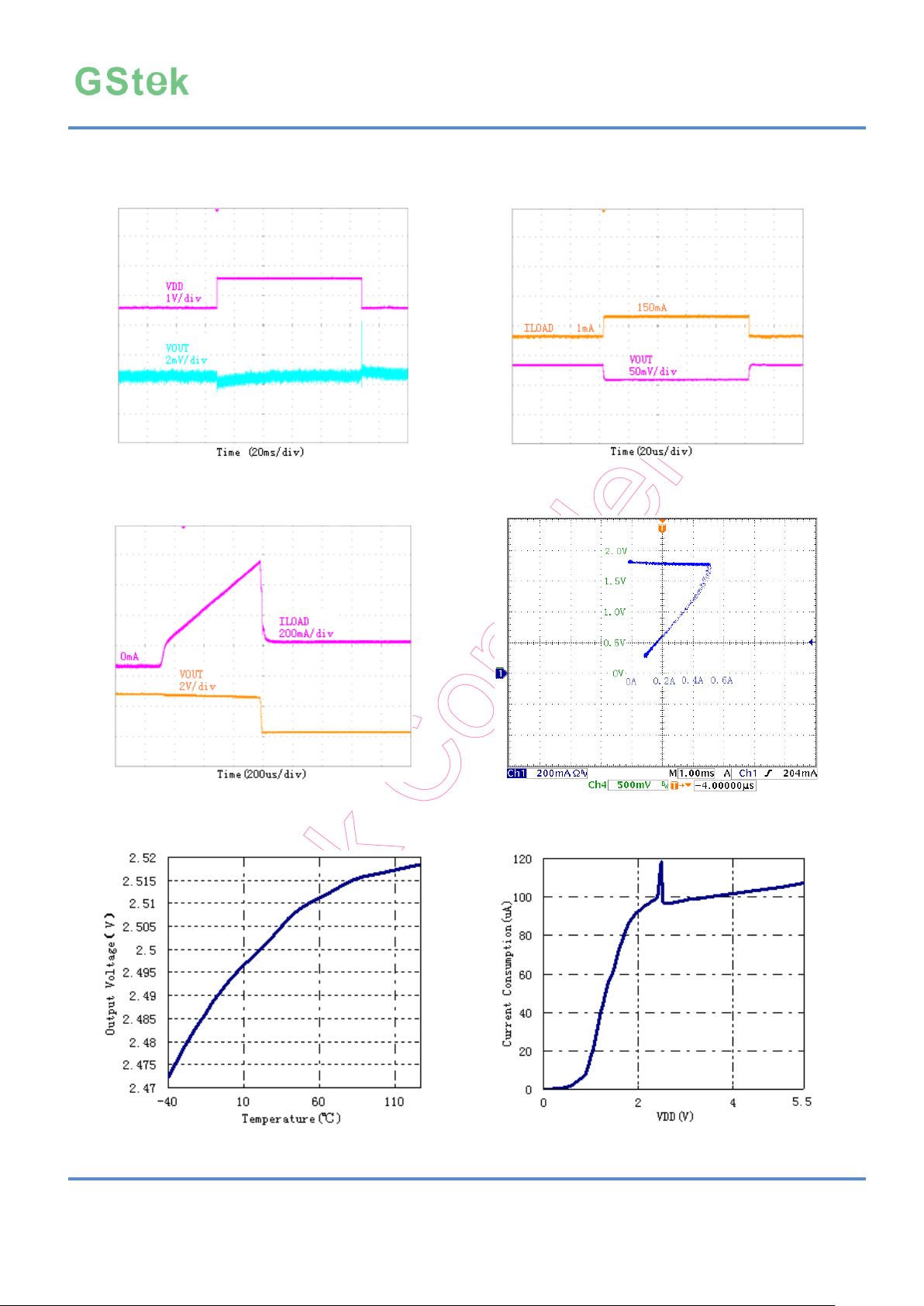
Line transient
Load transient
V
OUT
=2.5V,I
LOAD
=10mA, VDD=4.5V~3.5V~4.5V,tr=tf=10us
V
OUT
=2.5V,VDD=3.5,I
LOAD
=1mA~150mA~1mA,tr=tf=0.5us
Over current protection characteristics
Output Short Current
V
OUT
=2.5V, VDD=3.5V
V
OUT
=1.8V
Output voltage vs. temp
Current Consumption vs. VDD
V
OUT
=2.5 V, I
LOAD
=1mA, VDD=3.5
V
OUT
=2.5V, VDD=3.5, no load (FIX)
Typical Characteristics
Green Solution Technology Co.,LTD.
Rev.:1.72 8 Jan-17
Page 9
300mA, Fast Transient Response LDO Regulator GS7132
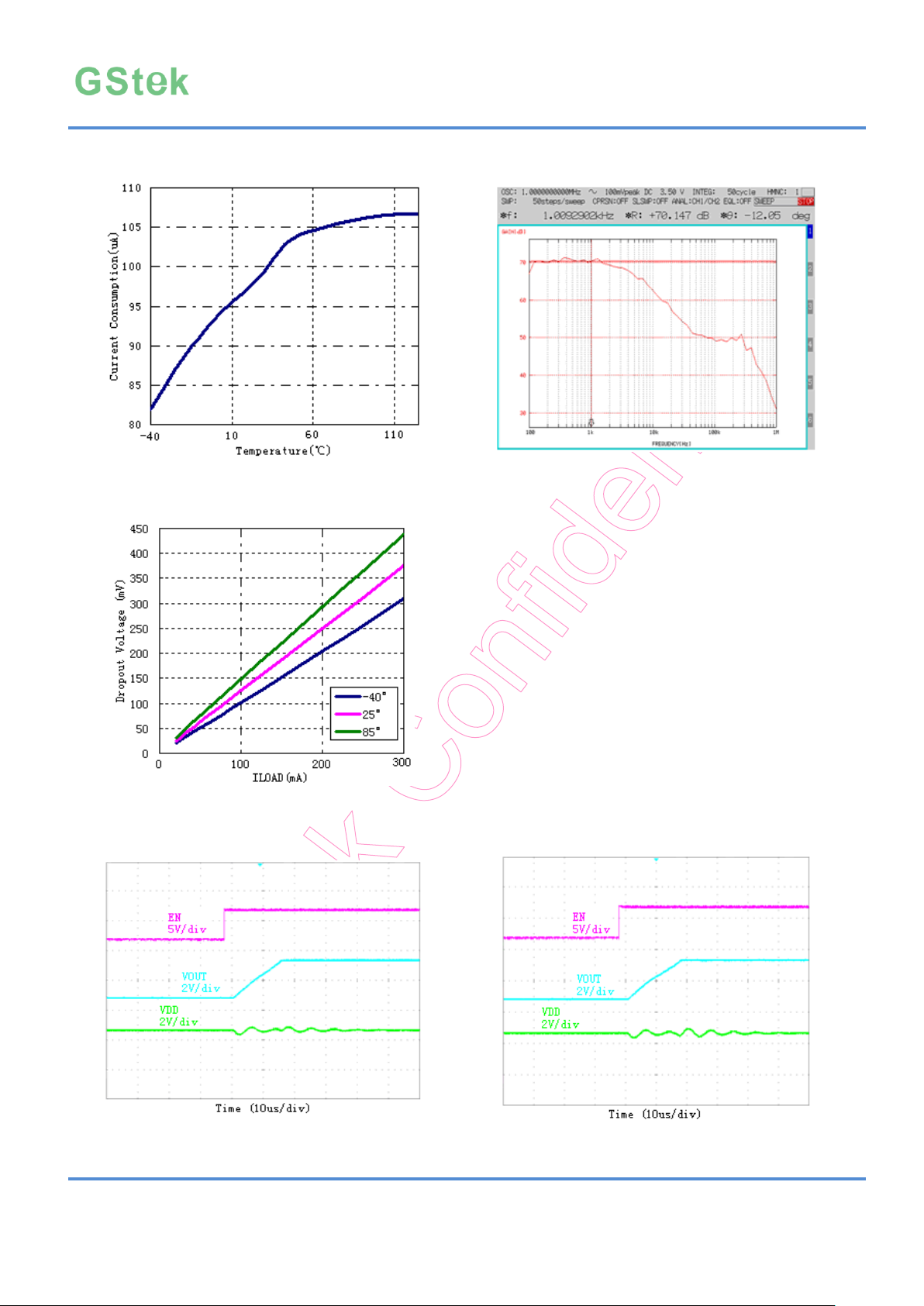
Current Consumption vs. temperature
PSRR vs. frequency
V
OUT
=2.5V, VDD=3.5,no load(FIX)
Dropout voltage vs. ILOAD
V
OUT
=2.5V
V
OUT
=2.5 V, VDD=3.5, I
LOAD
=1mA, Vpp=0.2V
Turn On Speed with EN pin(No Load)
Turn On Speed with EN pin(50mA Load)
V
OUT
=2.5V, VDD=3.5,no load
V
OUT
=2.5V, VDD=3.5, I
LOAD
=50mA
Green Solution Technology Co.,LTD.
Rev.:1.72 9 Jan-17
Page 10
300mA, Fast Transient Response LDO Regulator GS7132
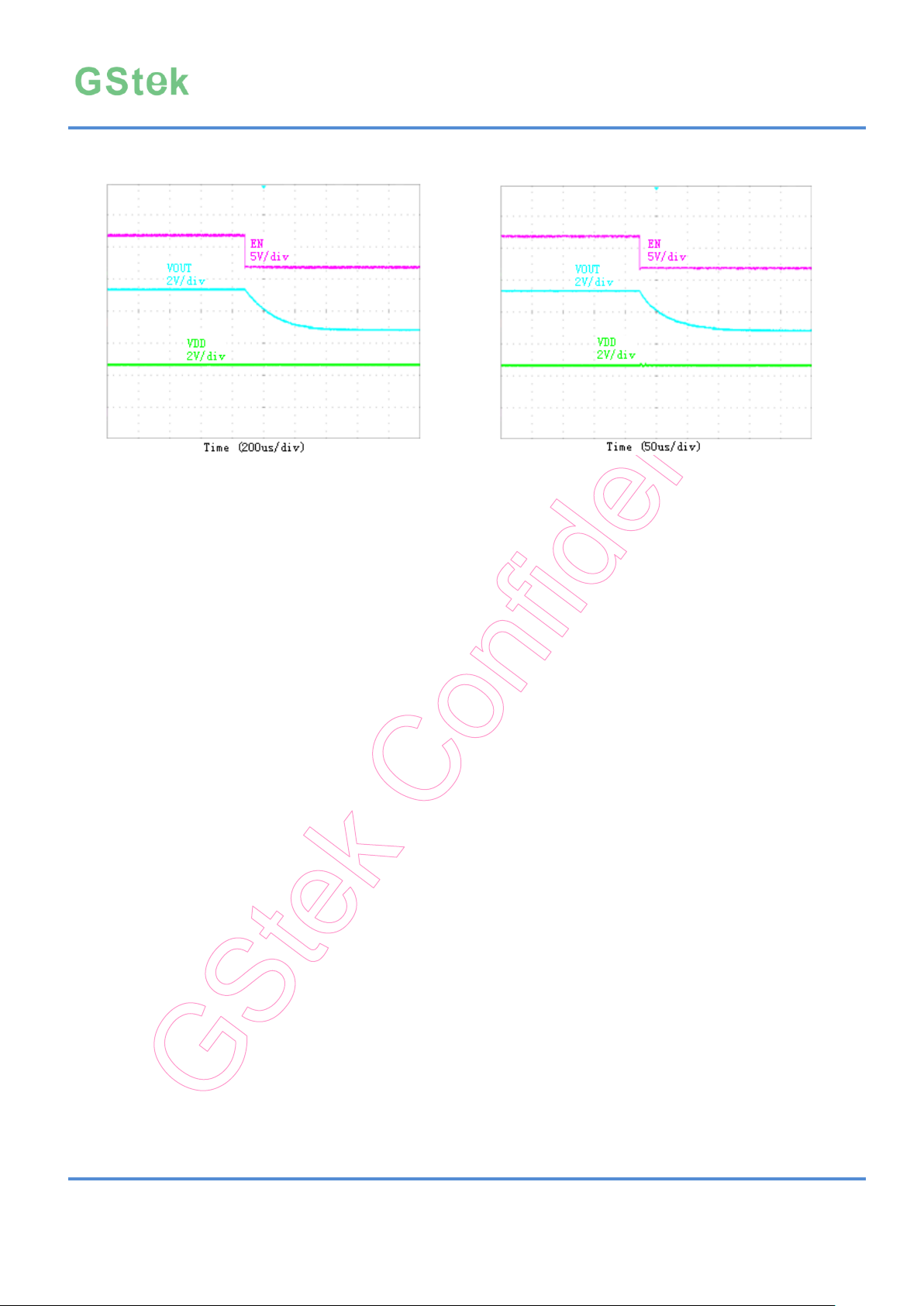
Turn Off Speed with EN pin(No Load)
Turn Off Speed with EN pin(50mA Load)
V
OUT
=2.5V, VDD=3.5,no load
V
OUT
=2.5V, VDD=3.5, I
LOAD
=50mA
Green Solution Technology Co.,LTD.
Rev.:1.72 10 Jan-17
Page 11

300mA, Fast Transient Response LDO Regulator GS7132
Application Information
Enable
dimensions’ capacitor.
The GS7132 has a dedicated enable pin(EN). When
the EN pin is in the logic low (VEN<0.3V), the
regulator will be turned off, reducing the supply
current to less than 1uA.
When the EN pin is in the logic high (VEN>1.2V),
the regulator will be turned on. Left open, the EN pin
is pulled down by a internal resistor to shut down the
regulator.
Current Limit
The GS7132 contains a foldback over current
protection function. It allows the output current to
reach the maximum value of 0.5A. Then further
decreases in the load resistance reduce both the
load current and the load voltage. The main
advantage of foldback limiting is less power
dissipation in the pass transistor under shorted- load
conditions.
Input Capacitor
Good bypassing is recommended from input to
ground to help improve AC performance. A 1uF
(X7R) input capacitor or greater located as close as
possible to the IC is recommended. Place the
capacitors physically as close as possible to the
device with wide and direct PCB traces.
Power Dissipation and Layout Considerations
Excessive power dissipation may cause thermal
overload, and hence the increase of the IC junction
temperature beyond a safe operating level. For
continuous operation, it is highly recommended to
keep the junction temperature below the maximum
operation junction temperature 125°C for maximum
reliability.
The relationship between θ
and T
JA
J(MAX)
can be
calculated as:
Output Capacitor
The GS7132 is specifically designed to employ
ceramic output capacitors as low as 1uF (X7R). The
ceramic capacitors offer significant cost and space
savings, along with high frequency noise filtering.
Place the capacitors physically as close as possible
to the device with wide and direct PCB traces.
Ceramic capacitors have different temperature
characteristics and bias characteristics which
depend on their dimensions and manufacturers. If
the setting voltage is 2.5V or more and the
capacitor’s dimensions for V
is too small, the
OUT
capacitance value might be extremely low. As a
result, the capacitance might be much less than
expected value. In such cases, the operation might
be unstable at low temperature (-25°C or less). In
that case, use a larger capacity, or a large
P
Where T
D(MAX)
= ( T
J(MAX)
− TA ) / θJA
J(MAX)
is the maximum operation junction
temperature 125°C, TA is the ambient temperature
and the θ
is the junction to ambient thermal
JA
resistance.
The power dissipation definition in device is:
PD = (VDD − V
OUT
) x I
+ VDD x IQ
OUT
As the above equations indicate, it is desirable to
work ICs whose θ
T
does not increase strongly with PD. To avoid
J(MAX)
values are small such that
JA
thermally overloading the GS7132, refrain from
exceeding the absolute maximum junction
temperature rating of 150°C under continuous
operating condition. Overstressing the regulator with
high loading currents and elevated input-to-output
differential voltages can increase the IC die
temperature significantly.
Green Solution Technology Co.,LTD.
Rev.:1.72 11 Jan-17
Page 12
300mA, Fast Transient Response LDO Regulator GS7132
D
E
e
1
2
3
4
Top View
Bottom View
Detail A
Pin #1 ID Options
Note:The configuration of the Pin#1 identifier is
optional,but must be located within the zone indicated.
Side View
See Detail A
1
1
L
b
D2
E2
A1
A
A3
pin 1 dot
b1
L1
Symbol
Dimensions in
Millimeters
Min
Max A 0.45
0.60
A1
0.00
0.05
A3
0.10
0.152
b
0.15
0.30
b1
0.02
0.12
D
0.90
1.10
D2
0.40
0.60
E
0.90
1.10
E2
0.40
0.60
e
0.65 REF.
L
0.20
0.30
L1
0.02
0.12
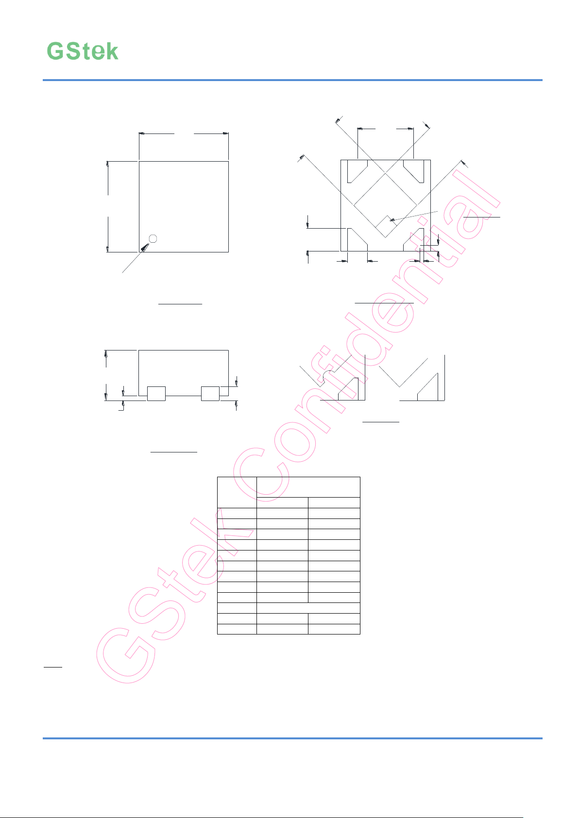
Package Dimensions, uDFN4-1x1
Note
1.Min.: Minimum dimension specified.
2.Max.: Maximum dimension specified.
3.REF.: Reference. Normal/Regular dimension specified for reference.
Green Solution Technology Co.,LTD.
Rev.:1.72 12 Jan-17
Page 13
300mA, Fast Transient Response LDO Regulator GS7132
A
L
DETAIL A
DETAIL A
c
A3
A1
e1
e
E
E1
D
b
5
4
1
2
3
Symbol
Dimensions in
Millimeters
Min.
Max.
A
0.90
1.45
A1
0.00
0.15
A3
0.90
1.30
b
0.30
0.50
c
0.08
0.25
e
0.95 REF.
e1
1.90 REF.
D
2.90 REF.
E
2.80 REF.
E1
1.60 REF.
L
0.30
0.60 θ 0o
8o
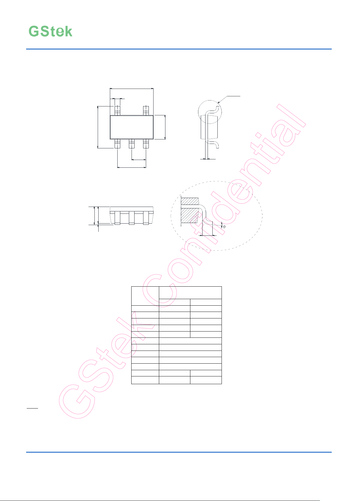
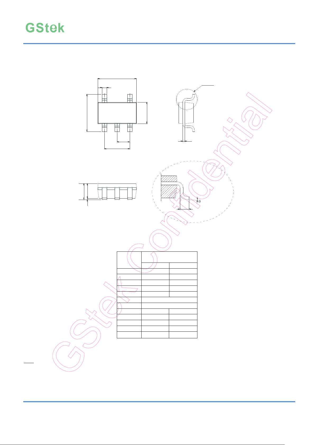
Package Dimensions, SOT-23-5
˙
Note
1.Min.: Minimum dimension specified.
2.Max.: Maximum dimension specified.
3.REF.: Reference. Normal/Regular dimension specified for reference.
Green Solution Technology Co.,LTD.
Rev.:1.72 13 Jan-17
Page 14
300mA, Fast Transient Response LDO Regulator GS7132
A
L
DETAIL A
DETAIL A
c
A3
A1
e1
e
E
E1
D
b
5
4
1
2
3
Symbol
Dimensions in
Millimeters
Min.
Max.
A
0.85
1.10
A1
0.00
0.10
A3
0.80
1.00
b
0.15
0.35
c
0.08
0.15
e
0.65 REF.
e1
1.30 REF.
D
2.00
2.20
E
2.15
2.45
E1
1.15
1.35
L
0.26
0.46 θ 0o
8o
Package Dimensions, SOT-353(SC-75)
Note:
1.Min.: Minimum dimension specified.
2.Max.: Maximum dimension specified.
3.REF.: Reference. Normal/Regular dimension specified for reference.
Green Solution Technology Co.,LTD.
Rev.:1.72 14 Jan-17
Page 15
300mA, Fast Transient Response LDO Regulator GS7132
A
L
DETAIL A
DETAIL A
c
A3
A1
e1
e
E
E1
D
b
1
2
3
Symbol
Dimensions in
Millimeters
Min.
Max.
A
0.90
1.15
A1
0.00
0.10
A2
0.90
1.05
b
0.30
0.50
c
0.08
0.15 e 0.95 REF.
e1
1.90 REF.
D
2.90 REF.
E
2.40 REF.
E1
1.30 REF.
L
0.30
0.50 θ 0o
8o
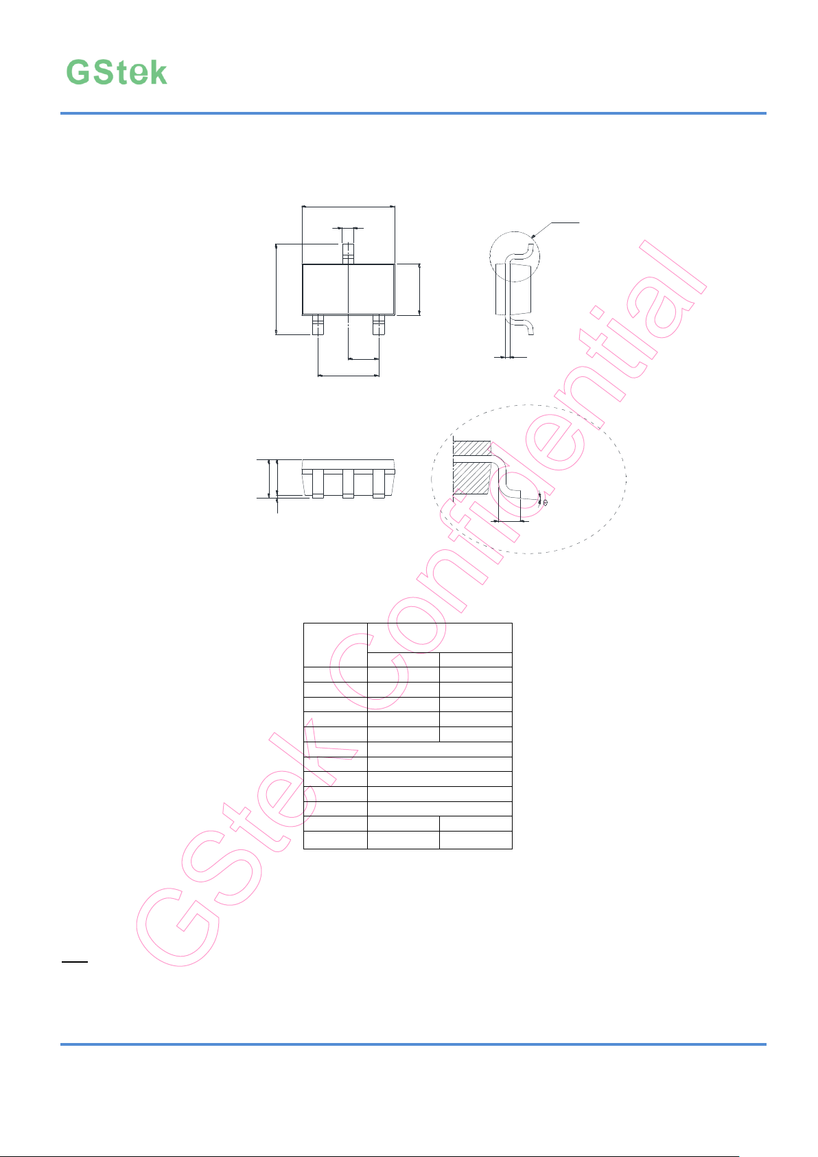
Package Dimensions, MSOT-23
Note
˙
1. Min.: Minimum dimension specified.
2. Max.: Maximum dimension specified.
3. REF.: Reference. Normal/Regular dimension specified for reference.
Green Solution Technology Co.,LTD.
Rev.:1.72 15 Jan-17
Page 16
300mA, Fast Transient Response LDO Regulator GS7132
Symbol
Dimensions in
Millimeters
Min.
Max.
A
1.40
1.60
A1
0.30
0.50
b
0.36
0.56
b1
0.41
0.53
C
0.35
0.44
D
4.40
4.60 E -
4.25
E1
2.30
2.60 e 1.50 REF.
L
0.80
1.10
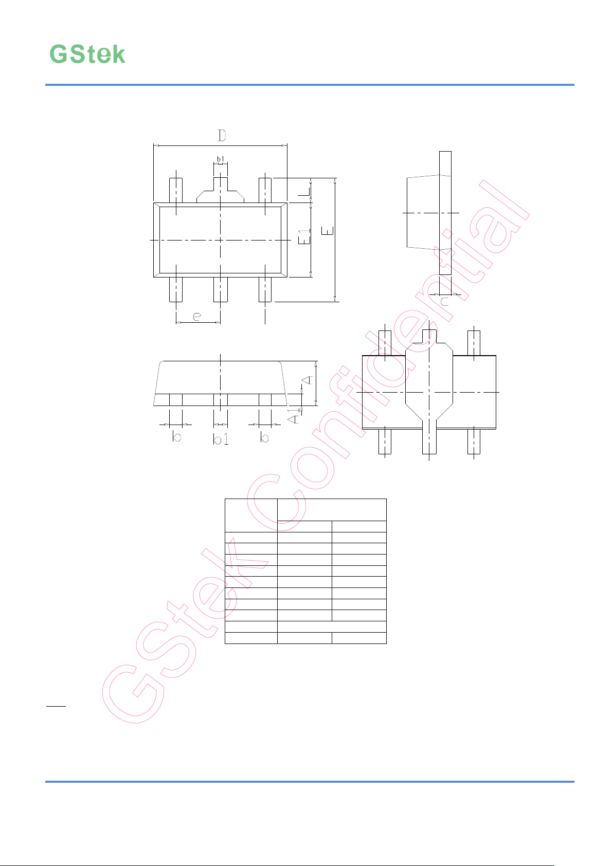
Package Dimensions, SOT-89-5
Note.
1.Min.: Minimum dimension specified.
2.Max.: Maximum dimension specified.
3.REF.: Reference. Normal/Regular dimension specified for reference.
Green Solution Technology Co.,LTD.
Rev.:1.72 16 Jan-17
Page 17
300mA, Fast Transient Response LDO Regulator GS7132
D
Pin 1 dot
A3
See Detail A
Detail A
Pin #1 ID Options
Note:The configuration of the Pin#1 identifier is
optional,but must be located within the zone indicated.
Top view
Bottom view
Side view
E
E1
L
D1
b
e
A1
A
Symbol
Dimensions in
Millimeters
Min.
Max.
A
0.70
0.80
A1
0.00
0.05
A3
0.203 REF.
b
0.18
0.35 e 0.65 REF.
D
1.90
2.10
E
1.90
2.10
D1
1.00
1.45
E1
0.50
0.85
L
0.25
0.45
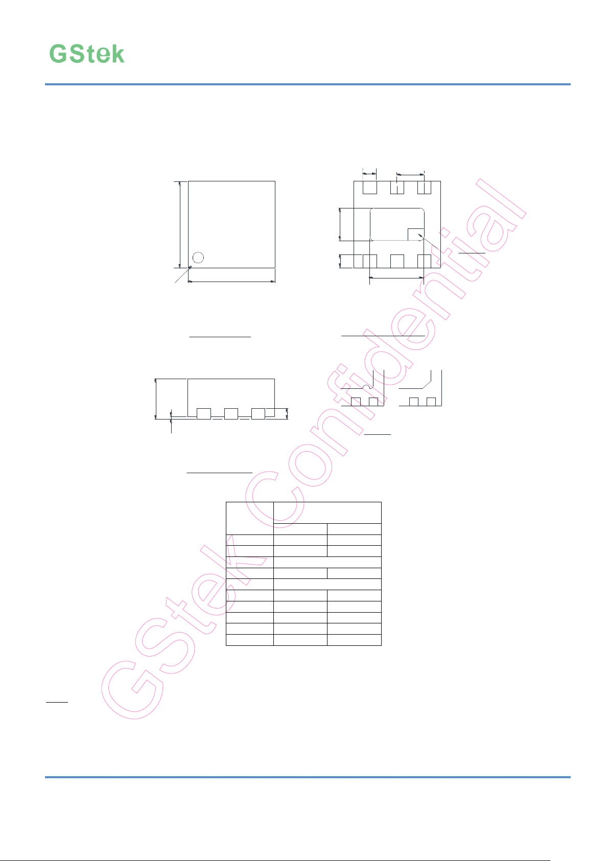
Package Dimensions, TDFN6-2x2
Note:
1. Min.: Minimum dimension specified.
2. Max.: Maximum dimension specified.
3. REF.: Reference. Normal/Regular dimension specified for reference.
Green Solution Technology Co.,LTD.
Rev.:1.72 17 Jan-17
Page 18

300mA, Fast Transient Response LDO Regulator GS7132
DISCLAIMERS
Please read the notice stated in this preamble carefully before Admission e accessing any contents of the
document attached. Admission of GStek’s statement therein is presumed once the document is released
to the receiver.
Notice:
Firstly, GREEN SOLUTION CO., LTD. (GStek) reserves the right to make corrections, modifications, enhancements, improvements, and
other changes to its information herein without notice.. And the aforesaid information does not form any part or parts of any quotation or
contract between GStek and the information receiver.
Further, no responsibility is assumed for the usage of the aforesaid information. GStek makes no representation that the interconnect
of its circuits as described herein will not infringe on exiting or future patent rights and other intellectual property rights, nor do the
descriptions contained herein express or imply that any licenses under any GStek patent right, copyright, mask work right, or other GStek
intellectual property right relating to any combination, machine, or process in which GStek products or services are used.
Besides, the product in this document is not designed for use in life support appliances, devices, or systems where malfunction of this
product can reasonably be expected to result in personal injury. GStek customers’ using or selling this product for use in such applications
shall do so at their own risk and agree to fully indemnify GStek for any damage resulting from such improper use or sale.
At last, the information furnished in this document is the property of GStek and shall be treated as highly confidentiality; any kind of
distribution, disclosure, copying, transformation or use of whole or parts of this document without duly authorization from GStek by prior
written consent is strictly prohibited. The receiver shall fully compensate GStek without any reservation for any losses thereof due to its
violation of GStek’s confidential request. The receiver is deemed to agree on GStek’s confidential request therein suppose that said receiver
receives this document without making any expressly opposition. In the condition that aforesaid opposition is made, the receiver shall
return this document to GStek immediately without any delay.
Green Solution Technology Co.,LTD.
Rev.:1.72 18 Jan-17
 Loading...