


™
PRO-LINX
GS7005
Complete Serial Digital Video Receiver
DATA SHEET
FEATURES
• SMPTE 259M-C compliant
• fully integrated 270 Mb/s SDI receiver
• integrated cable equa lization (10 0m Belden 8 281 typica l)
• low power consumption (750mW typical)
• operates from 0°C to 85°C
• small footprint with minimal external components
• Lock and Carrier Detect output indications
• H timing signal output
• SMPTE descrambler and NRZI decoder may be
disabled for DVB - ASI applications
• ease of design use and adjustment free operation
APPLICATIONS
Limited space, low power SMPTE 259M-C or generic
270Mb/s serial to parallel interfaces; DVB-ASI 270Mb/s
receive interface; broadcast quality uncompressed video
interface for industrial and professional video equipment
such as video editing workstations.
DESCRIPTION
The GS7005 is a BiCMOS integrated circuit capable of
operating as a complete 270Mb/s Serial Digital Video
receiver. The GS7005 provides a complete serial digital
video receive solution while consuming only 750mW.
The serial data input accepts SMPTE 259M-C compliant
signals. An on-chip by-passable equalizer typically provides 100m of co-axial cable equalization. The clock
recovery is performed on chip with minimal external
components. The incoming serial data is decoded using an
NRZI decoder and SMPTE descrambler to provide SMPTE
125M compliant 27Mb/s parallel data outputs and clock.
ORDERING INFORMATION
PART NUMBER PACKAGE TEMPERATURE
GS7005 - CQT 52 pin MQFP 0°C to 85°C
GS7005 - CTT 52 pin MQFP Tape 0°C to 85°C
GS7005
C
1C2
LOCK
CD
SDI
SDI
SIGNAL
LOCK
DETECT
EQUALIZER
EQ
SLICER
MUX
NRZI
DECODER
DESCRAMBLER
SMPTE
f/10PLL
TRS
DETECTOR
S to P
PCLK
OUT
H
D
OUT[9:0}
10
BLOCK DIAGRAM
Revision Date: January 2001 Document No. 522 - 14 - 06
GENNUM CORPORATION P.O. Box 489, Stn. A, Burlington, Ontario, Canada L7R 3Y3
Tel. +1 (905) 632-2996 Fax. +1 (905) 632-5946 E-mail: info@gennum.com
www.gennum.com
ABSOLUTE MAXIMUM RATINGS
PARAMETER VALUE
Supply Voltage 5.5V
Input Voltage Range (any input) GND < V
IN
< V
DC Input Current (any one input) 10mA
Power Dissipation (V
= 5.25V) 1W
CC
Maximum Die Temperature 125°C
Operating Temperature Range 0°C <= T
Storage Temperature Range -65°C <= T
<= 85°C
A
<= 150°C
S
Lead Temperature (soldering 10s) 260°C
DC ELECTRICAL CHARACTERISTICS
VCC = 5V, TA = 25°C, unless otherwise specified.
Serial data rate = 270Mb/s, Parallel Data Rate = 27Mb/s, ƒ
PARAMETER SYMBOL CONDITIONS MIN TYP MAX UNITS NOTES TEST LEVEL
Positive Supply Voltage V
CC
Power Consumption P V
Supply Current
Logic Inputs - Low V
Logic Inputs - High V
I
CC
IL
IH
= 27MHz
PCLK
Operating
range
= 5.25V - 750 - mW 5
CC
VCC = 5.25V - 140 - mA 1
VCC = 5.25V - - 0.8 V 6
VCC = 4.75V 2 - - V 6
CC
GS7005
4.75 5.00 5.25 V 6
Logic Outputs - Low V
Logic Outputs - High V
OL
OH
VCC = 5.25V - - 0.5 V 1
VCC = 4.75V 2.4 - - V 1
TEST LEVELS
1. Production test at room temperature and nominal supply voltage with guardbands for supply and temperature ranges.
2. Production test at room temperature and nominal supply voltage with guardbands for supply and temperature ranges using
correlated test.
3. Production test at room temperature and nominal supply voltage.
4. QA sample test.
5. Calculated result based on Level 1,2, or 3.
6. Not tested. Guaranteed by design simulations.
7. Not tested. Based on characterization of nominal parts.
8. Not tested. Based on existing design/characterization data of similar product.
GENNUM CORPORATION
2
522 - 14 - 06
AC ELECTRICAL CHARACTERISTICS
VCC = 5V, TA = 25°C, unless otherwise specified in ‘conditions’
Serial data rate = 270Mb/s, Parallel Data Rate = 27Mb/s, ƒ
PARAMETER SYMBOL CONDITIONS MIN TYP MAX UNITS
PCLK
= 27MHz
NOTESTEST
LEVEL
Parallel Data - Rise/Fall Time t
PCLK Rising Edge to D
Centre t
OUT(N)
PCLK Rise/Fall Time t
R/F_DOUT
D
R/F_PCLKOUT
Input Return Loss LOSS
IN
CL = 20pF 1.0 - 6.0 ns 1 4, 7
- - ±5 ns 2, 3 4, 7
CL = 20pF 0.5 - 3.0 ns 1 4, 7
75Ω match
-17 - dB 7
5MHz to 270MHz
Asynchronous Lock Time t
Synchronous Lock Time t
LOCK_ASYNC
LOCK_SYNC
Input Jitter Tolerance t
Output PCLK Jitter t
J_PCLKOUT
J_SI
Pathological Input - 0.35 - U.I. 6 7
Pseudorandom
- - 250 ms 4 1
- - 10 µs 5 1
- 800 - ps p-p 1
Input
Pathological Input - 1000 - ps p-p 6 7
Error Free Cable Length Pseudorandom
- 100 - m 7
Input
Pathological Input 75 100 - m 6, 7 1
NOTES
1. Rise/Fall time is defined as the time for the signal to rise from 20% to 80% of the specified p-p value, or to fall from 80% to 20% of the
specified value.
2. Refer also to Figure 10.
3. This is the time difference between the rising edge of PCLK
and the centre of the bit period.
OUT
4. This is the time delay between a valid serial TRS signal on the input to the moment valid data appears on the parallel outputs.
5. This is the time for the PLL to re-lock when video streams are switched during the vertical blanking interval in accordance with SMPTE
RP168-1993. The two streams may be 180° out of phase with respect to one another, but pixel aligned.
6. This pathological pattern is defined in SMPTE RP178-1996, paragraphs 4.1 and 4.3.
7. "Error free" is defined as no single bit errors over a period of 10 minutes, using Belden 8281 Cable and 75Ω connections. The MIN
value is fully tested and the TYP value is based on using the EB7005 Evaluation Board.
GS7005
TEST LEVELS
1. Production test at room temperature and nominal supply voltage with guardbands for supply and temperature ranges.
2. Production test at room temperature and nominal supply voltage with guardbands for supply and temperature ranges using correlated
test.
3. Production test at room temperature and nominal supply voltage.
4. QA sample test.
5. Calculated result based on Level 1,2, or 3.
6. Not tested. Guaranteed by design simulations.
7. Not tested. Based on characterization of nominal parts.
8. Not tested. Based on existing design/characterization data of similar product.
3
GENNUM CORPORATION
522 - 14 - 06
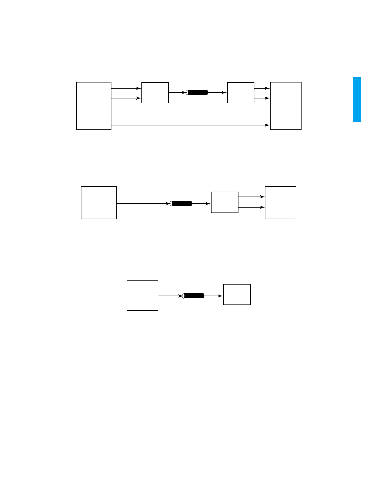
TEST SETUP
TEKTRONIX
GigaBERT
1400
TRANSMITTER
TEKTRONIX
VIDEO SlGNAL
GENERATOR
DATA
DATA
CLOCK
VIDEO STREAM
WITH EDH
BELDEN 8281
GS9028
CABLE
DRIVER
CABLE
EB7005
BOARD
Fig. 1a T est Setup for Jitter Measurements
BELDEN 8281
CABLE
EB7005
BOARD
Fig. 1b Test Setup for Error-Free Cable Length
GS7005
TEKTRONIX
TDS 820
SCOPE
TRIGGER
EB9021
EDH ERROR
COUNTER
GENNUM CORPORATION
BELDEN 8281
HP 4195A
NETWORK
ANALYSER
CABLE
EB7005
BOARD
Fig. 1c T est Setup for Return Loss Measurements
4
522 - 14 - 06

PIN CONNECTIONS
OUT
RSVD1
RSVD1
GS7005
TOP VIEW
1C2
C
CC3
V
CC1
V
CD
SDI
SMPTE
RSVD0
SDI
CC2
V
RSVD0
PCLK
GND
RSVD0
VDDGND
EQ
RSVD1
GND
39
38
37
36
35
34
33
32
31
30
29
28
27
GND
GND
D
OUT0
D
OUT1
D
OUT2
D
OUT3
D
OUT4
D
OUT5
D
OUT6
D
OUT7
D
OUT8
D
OUT9
LOCK
GND
NOTE: RSVD = Reserved
GND
GND
52 51 50 49 48 47 46 45 44 43 42 41 40
1
GND
GND
2
3
4
5
6
7
8
9
10
11
12
H
13
14 15 16 17 18 19 20 21 22 23 24 25 26
GND
GND
RSVD0
RSVD0
RSVD0
RSVD0
RSVD0
RSVD0
RSVD0
RSVD0
RSVD0
RSVD0
PIN DESCRIPTIONS
NUMBER SYMBOL TYPE DESCRIPTION
1, 13, 14, 26, 27,
39, 40, 52
2-11, 22, 44, 45 RSVD0 - Connect to Ground.
12 H O H Indication. HIGH after EAV ID and LOW after SAV ID.
15 GND - Ground for analog blocks of the device.
16, 17 C
18 V
19, 20 SDI, SDI
21 V
23 GND - Ground for PECL blocks of the device.
24 EQ
25, 49, 50 RSVD1 - Connect to V
28 LOCK O Signal Lock Indication Output. Goes HIGH approximately 38µs after valid parallel data
29-38 D
41 GND - Ground for CMOS blocks of the device.
42 V
43 PCLK
46 SMPTE
47 CD
48 V
51 GND - Ground for analog and PECL blocks of the device.
GND - Connect to Ground.
1
, C
CC1
2
- External 100nF loop filter capacitor connection.
- Power supply for analog blocks of the device.
I Differential Serial Data Input
CC2
- Power supply for PECL blocks of the device.
I Equalizer Control; LOW = EQ on, HIGH = EQ bypassed.
CC.
occurs.
OUT[9:0]
DD
OUT
O 27Mb/s Parallel Data Outputs.
- Power supply for CMOS blocks of the device.
O 27MHz Clock Output.
I NRZI decoding and descrambling control.
LOW = NRZI and SMPTE mode on. HIGH = NRZI and SMPTE mode disabled.
O Carrier Detect. Active LOW. Goes LOW when carrier is detected and high when carrier is
lost.
CC3
- Power supply for Analog and PECL blocks of the device.
GS7005
GENNUM CORPORATION
5
522 - 14 - 06

INPUT / OUTPUT CIRCUITS
V
DD
ESD
GS7005
IN
GND
Fig. 2 SDI, SDI
V
DD
TO INTERNAL
STRUCTURES
ESD
TO INTERNAL
STRUCTURES
Fig. 3 D
ESD
TTL-IN
GND
, H, LOCK, CD, PCLK
OUT[9:0]
V
DD
TO INTERNAL
STRUCTURES
GND
OUT
OUT
GENNUM CORPORATION
Fig. 4 EQ, SMPTE
6
522 - 14 - 06

TYPICAL PERFORMANCE CURVES
0
(V
= 5V, TA = 25°C unless otherwise shown)
CC
J1
J2
J0.5
-10
-20
-30
270MHz
135MHz
RETURN LOSS (dB)
-40
-50
0.05 GHz 1 GHz
FREQUENCY (GHz)
Fig. 5 Input Return Loss
0
600kHz
-3
AMPLITUDE (dB)
-6
1k 10k 100k 1M 10M
FREQUENCY (Hz)
54MHz
1.97GHz
540MHz
Impedances
normalized
to 50
W
-J0.5
-J1
Fig. 7 Input Impedance
800
700
600
500
400
300
POWER (mW)
200
100
0
0 10 20 30 40 50 60 70 80 90
TEMPERATURE (˚C)
GS7005
270MHz
-J2
GENNUM CORPORATION
Fig. 6 Loop Bandwidth
Fig. 8 Power vs. Temperature
7
522 - 14 - 06

RECEIVER OPERATION
EQ SMPTE GS7005 Operating mode
0 0 SMPTE 259M Receiver (Equalizer ON, SMPTE / NRZI Descrambler enabled).
1 0 SMPTE 259M Receiver with equalizer bypassed.
0 1 Receiver function with equalizer enabled and NRZI and SMPTE Descrambler disabled.
1 1 Receiver function with equalizer bypassed and NRZI and SMPTE Descrambler disabled.
The output of the LOCK pin is logic high approximately
38µs after the receiver has successfully locked to the input
serial bit stream. The output H is set low after the SAV ID
and is set high after the EAV ID when these sequences are
identified in the incoming bit stream.
If external equalization is performed prior to this device,
bypass the equalization control function (EQ
) by setting it
HIGH.
To turn off the NRZI and SMPTE Descrambler function, set
SMPTE
HIGH. When operating in this mode, the output of H
is either "1" or "0" (indeterminate).
DIAGRAMS
The figure below shows the timing relationship between the outputs of the GS7005.
PCLK
D
OUT
OUT[9:0]
H
XXX XXX 3FF 000 000
Fig. 9 Timing Diagram for Parallel Outputs, PCLK
XXX XXX XXX XXX XXX XXX 3FF 000 000 EAV ID XXX XXX
SAV ID
...
...
...
, and H
OUT
The figure below shows the relationship between the parallel clock and the parallel data outputs. The rising edge of the
parallel clock is within ±5ns of the centre of the data.
GS7005
D
OUT[9:0]
PCLK
WORD CENTRE
5ns
5ns
OUT
Fig. 10 Parallel Clock Alignment
GENNUM CORPORATION
8
522 - 14 - 06

DETAILED DESCRIPTION
The main functional blocks of the GS7005 are:
1. PECL input buffer
signal by applying the same algorithm to the received
signal. For data structures that do not require descrambling and NRZI-NRZ conversion, bypass this block
by setting the SMPTE
pin to logic HIGH.
2. Fixed Gain Equalizer
3. Slicer
4. NRZI Decoder & SMPTE Descrambler
5. TRS Detector
6. Signal Lock Detect
7. Serial to Parallel Convertor
Refer to the Functional Block Diagram on the front page of
this data sheet.
1. PECL INPUT BUFFER
This differential input buffer features a built-in load
termination for the incoming SDI signal. The load is
characterized as 75Ω over a wide frequency range and is
made up of an internal fixed resistor and current source.
2. FIXED GAIN EQUALIZER
The Fixed Gain Equalizer stage is used to compensate the
frequency dependent loss of the SDI signal through co-axial
cable. The SDI signal is connected to the input pins (SDI/
SDI
) either differentially or single ended. The input signal
passes through a fixed gain equalizing stage whose
frequency response closely matches the inverse cable loss
characteristic. The equalizer typically provides 100m of
coaxial cable equalization. The frequency response is
optimized for maximum cable length. For short cable
lengths (<10m), bypass the equalizing stage by setting the
EQ control pin to a logic HIGH level. If an external equalizer
is used, bypass the internal equalizer of the GS7005 to
avoid over-equalization (
3. POST EQUALIZATION SLICER
see Figure 12
).
The Post Equalization Slicer stage slices the equalized
signal, thereby eliminating any DC offset due to the AC
coupling requirement of the SDI signal. Using a differential
comparator, the received signal voltage is compared to a
midway voltage, known as the baseline or the slicing level.
The sliced signal is then applied to the NRZI/SMPTE
Decoder/Descrambler and the PLL MUX.
4. NRZI DECODER & SMPTE DESCRAMBLER
To comply with the the ANSI/SMPTE 259M standard, use a
scrambled, polarity free NRZI code. The polynomial
generator for the scrambler is G1(X) = X
9+X4
+1. The NRZI
code is produced by a second polynomial, G2(X) = X+1.
The NRZI Decoder and SMPTE Descrambler blocks within
the GS7005 regenerate the original NRZ unscrambled
5. PLL, MUX and f/10
The PLL clock recovery circuitry provides an internal,
synchronous 270MHz clock. The 27MHz parallel data clock
is derived from the serial clock through a resettable
frequency divider. To synchronize the parallel clock signal,
set the frequency divider to the initial state at the same time
the state machine has detected the Timing Reference
Signal (TRS).
The PLL self-centres the VCO to approximately 29MHz
when there are no input data transitions. This allows the PLL
to lock when a valid signal within the lock range is applied.
However, if the GS7005 detects a spurious input with
random data transitions, the centering function of the VCO
is inhibited. This causes the VCO control voltage to drift to a
low clamp level resulting in a VCO frequency of 22MHz. To
prevent this “latch-up” condition implementation of a high
impedance (1MΩ) bleed resistor across the C1 and C2
(loop filter, pins 16 and 17) is recommended. Due to the
large resistance value, the effect on IJT is negligible (
Figure 11
6. TRS DETECTOR
).
see
The TRS Detector detects the TRS headers (EAV and SAV).
It consists of a word-counter, bit-counter and control statemachine. The bit-counter is reset by either the decoded
data or the output of the state-machine. In a normal case,
the state-machine output is LOW. The reset of the bit
counter is active LOW so that the bit-counter will be started
when the data is HIGH. The detection of a valid TRS header
is indicated by a level change of the H-signal pin.
7. SIGNAL LOCK DETECT
When there are no input data transitions, the CD pin goes to
a HIGH logic level and forces the VCO to the centre
frequency as described in section 5,
PLL, MUX, and f/10
This output can be used to control an external transistor
and LED. When there are input data transitions (valid or
invalid), the CD
pins goes to a LOW logic state.
The locking state of the PLL is indicated by the output
LOCK signal being set to a logical HIGH level. This pin
however, may have periodic transitions to a LOW logic state
of 64µs maximum duration even though the device is
properly locked. The parallel data signal integrity is not
affected under these conditions. Therefore, the LOCK pin
should not be used as a logic control signal if a steady level
is required. The output voltage remains in a logic HIGH
state for a sufficient period and can be used to drive visual
indicators such as LEDs.
GS7005
.
GENNUM CORPORATION
9
522 - 14 - 06

8. SERIAL TO PARALLEL CONVERTOR
The final function of the GS7005 is the serial-to-parallel
conversion. The output signals of the receiver are ten data
signals and one clock signal. The shift register is filled by
the serial data and read out at a positive edge of the readout signal. After parallel read out of the shift register, the
parallel data is sampled with the negative edge of the
27MHz clock to achieve synchronization.
GS7005
GENNUM CORPORATION
10
522 - 14 - 06

APPLICATION CIRCUITS
V
CC
220
CD
10k
100n
MODE
V
CC
52 51 50 49 48 47 46 45 44 43 42 41 40
CD
RSVD1
RSVD1
C1C2V
100n
CC3
V
GS7005
CC1
SDI
100n
GND
1
2
3
4
5
6
7
8
9
10
11
12
13
GND
RSVD0
RSVD0
RSVD0
RSVD0
RSVD0
RSVD0
RSVD0
RSVD0
RSVD0
RSVD0
H
GND
GND
GND
GND
14 15 16 17 18 19 20 21 22 23 24 25 26
1M
SERIAL DIGITAL
INPUT
Fig. 11 Application Circuit - Unbalanced Serial Input Operation
RSVD0
SMPTE
CC2
SDI
V
100n
V
CC
10µ10µ
V
CC
OUT
RSVD0
PCLK
RSVD0
GNDEQRSVD1
33
V
CC
100n
10p
100n
V
CC
V
CC
10µ
GS7005
DD
V
GND
GND
GND
D
OUT0
D
OUT1
D
OUT2
D
OUT3
D
OUT4
D
OUT5
D
OUT6
D
OUT7
D
OUT8
D
OUT9
LOCK
GND
GND
V
CC
39
38
37
36
35
34
33
32
31
30
29
28
27
10k
V
CC
EQ
PARALLEL
CLOCK OUT
PARALELL
DATA OUT
V
CC
220
LOCK
RSVD = Reserved.
All resistors in ohms,
all capacitors in farads,
unless otherwise shown.
100n
SERIAL
DIGITAL INPUT
10n
10n
75
37.5
V
CC1
10µ
10n
V
CC
75
75
V
10n
CC
OUTPUT EYE
MONITOR
GND
AGC
GND
V
CC
D
IN
D
IN
GND
V
CC
100n
TRISTATE
GS9024
75
1µ
V
CC
SSI-CD
13 12 11 10 9 8 7 6 5 4 3 2 1
H
GND
RSVD0
RSVD0
14
GND
15
GND
16
C
1
17
C
2
18
V
CC1
19
SDI
20
SDI
21
V
CC2
22
RSVD0
23
GND
24
EQ
25
RSVD1
26
GND
GND
27
28 29 30 31 32 33 34 35 36 37 38 39
10k
RSVD0
OUT9DOUT8DOUT7DOUT6DOUT5DOUT4DOUT3DOUT2DOUT1DOUT0
LOCK
D
PARALLEL DATA OUTPUTS
CD-ADJ
V
CC
AGC
D
D
OEM
10n
CD
OUT
OUT
10n
10n
1M
V
CC
100n
7575
100n
V
CC
475
2k
475
CC
100n
V
CC
V
CC
220
V
LOCK
Fig. 12 Typical Application Circuit with External Equalizer
RSVD0
RSVD0
RSVD0
RSVD0
GS7005
RSVD = Reserved.
All resistors in ohms,
all capacitors in farads,
unless otherwise shown.
RSVD0
RSVD0
PCLK
GND
RSVD0
GND
GND
RSVD1
RSVD1
V
CC3
CD
SMPTE
RSVD0
RSVD0
OUT
V
DD
GND
GND
GND
V
CC
220
V
CC
52
51
100n
CD
50
49
48
V
10k
CC
47
46
45
MODE
44
43
42
41
33
40
PCLK OUT
10p
V
CC
100n
GENNUM CORPORATION
11
522 - 14 - 06

PACKAGE DIMENSIONS
17.20 BSC
14.00 BSC
2.67
±0.08
0.25 MAX
0.10 MIN
1.00 BSC
0.50 MAX
0.35 MIN
All dimensions are in millimetres.
52 pin MQFP
BSC = Basic or nominal
14.00
BSC
0.18
±0.05
17.20
BSC
3.00 MAX
2.7
14 ±2˚
14 ±2˚
0.13 MIN.
RADIUS
1.60
REF
0.40 MIN
0˚ MIN
0.88
±0.15
0.13 MIN
RADIUS
7˚ MAX
0˚ MIN
GS7005
CAUTION
ELECTROSTATIC
SENSITIVE DEVICES
DO NOT OPEN PACKAGES OR HANDLE
EXCEPT AT A STATIC-FREE WORKSTATION
DOCUMENT IDENTIFICATION
DATA SHEET
The product is in production. Gennum reserves the right to make
changes at any time to improve reliability, function or design, in order to
provide the best product possible.
GENNUM CORPORATION
MAILING ADDRESS:
P.O. Box 489, Stn. A, Burlington, Ontario, Canada L7R 3Y3
Tel. +1 (905) 632-2996 Fax. +1 (905) 632-5946
SHIPPING ADDRESS:
970 Fraser Drive, Burlington, Ontario, Canada L7L 5P5
Gennum Corporation assumes no responsibility for the use of any circuits described herein and makes no representations that they are free from patent infringement.
REVISION NOTES:
Added label to package dimension drawing to show package
thickness and included the third view; Added information to
section 5,
PLL, MUX and f/10
; Removed Figures 5 and 6 “Data to Follow”; Added resistor to Figures 11 and 12; Added
to Package Dimensions legend.
For the latest product information, visit www.gennum.com.
GENNUM JAPAN CORPORATION
C-101, Miyamae Village, 2-10-42 Miyamae, Suginami-ku
Tokyo 168-0081, Japan
Tel. +81 (03) 3334-7700 Fax. +81 (03) 3247-8839
GENNUM UK LIMITED
25 Long Garden Walk, Farnham, Surrey, England GU9 7HX
Tel. +44 (0)1252 747 000 Fax +44 (0)1252 726 523
© Copyright November 1999 Gennum Corporation. All rights reserved. Printed in Canada.
12
522 - 14 - 06
 Loading...