

Page 1
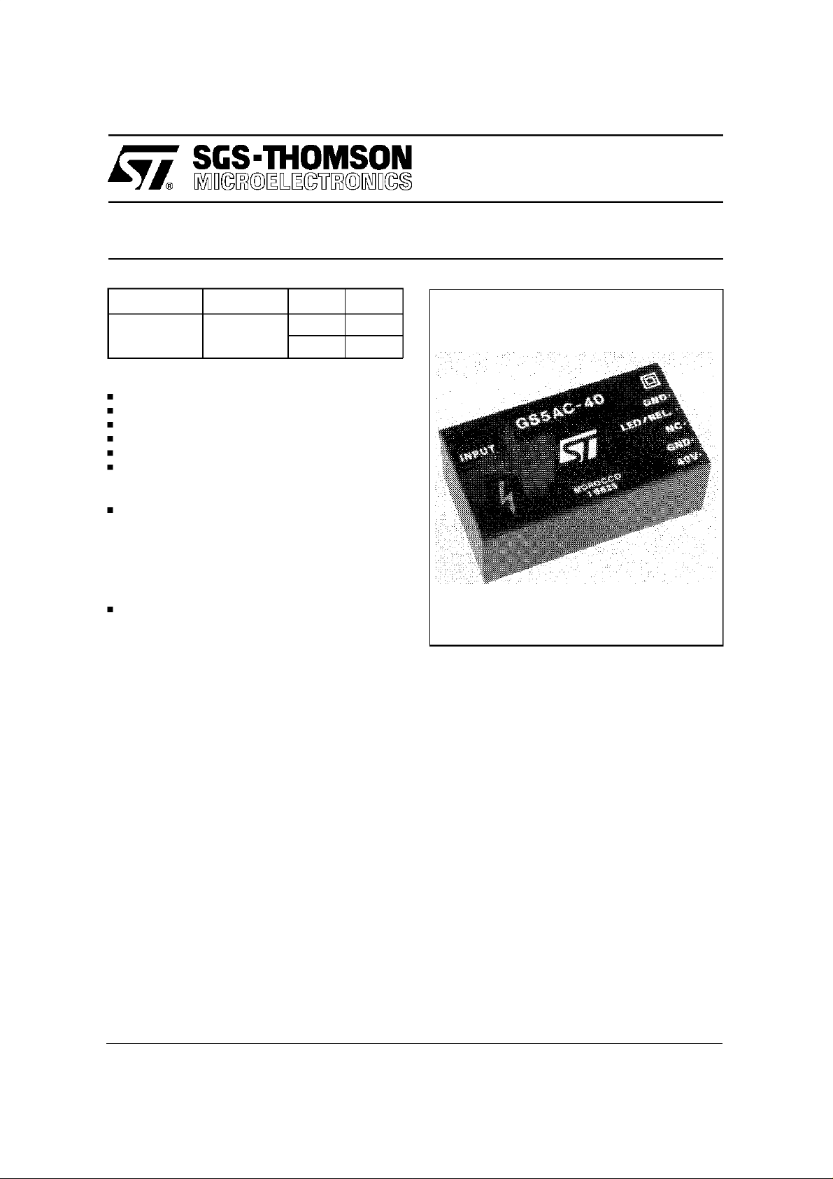
GS5AC-40
ISDN AC-DCCONVERTER
PRELIMINARYDATA
Type V
GS5AC-40 180 to 264V
i
V
o
out 1: 40V 110mA
out 2: 40V 10 mA
I
o
FEATURES
Large Input voltage range: 180 to 264 VRMS
Input filterto meet EMI requirements
Peakinput overvoltage whitstanding
Input fuse
Input to output insulation
2 insulated outputs:
Vo1= 35 to 42 V for ”S” interface
Vo2=36 to 47 V forexternalrelayand LED driver
”S” interface output characteristics:
Peakoutput of 8 W for 150 ms
Typical output power: 4,5 W
Output filtering to meet ETSI requirements
Holdup time: 20 mswith 4,5 Woutput power
Continuousshort circuit protection
Peak overvoltage withstand:250 V for 10/700µs
Mechanicaldimensions (LxWxH):80x43x30 mm
DESCRIPTION
The GS5AC-40 converter has been designed for
an ISDN-NTBA (Network Termination Basic Access) system with either 4B3T or 2B1Q standard
trasmission.
The converteris able to deliver 40V/110mA for ”S”
interface and is equipped also with asecond, auxiliary 40V/10 mA output for relay and LED driving.
The converteroffersshort-circuit protection onboth
outputs (short-circuit on 40V output doesn’t affect
relay/LED output and the input power never exceeds the limit of 15 W) and also provides to
remove the auxiliary(relay &LED) output when the
mains is missing,thus allowingthe useof a second
”emergency” voltage source (relay contacts are
released). 3000 V
insulation voltage for 60
RMS
secondsisprovided betweeninputandtheoutputs.
Output 1 and Output 2 share the same common
ground (pin 4 is internally connected with pin 6).
The design of the module has been conducted
using,as reference standards, the following:
EN 60950, VDE0878 part 1 class B (EMC),
EN55022classB (EMC), CCITT 430, ETS300012
and ETS 300 047 (ISDN BASIC ACCESS, Safety
and Protection);anyway,pleasenote that no certification processes have been carried out on the
moduleitself.
20 January1997 1/4
Page 2

GS5AC-40
ELECTRICAL CHARACTERISTICS (T
amb
Std. Conditions: Vin = 180 to 264 V
Po1 = 0 to 4.5 W Io2 = 0 to 10 mA Vo2= 36 to 47 V
Symbol
Input Voltage
V
i
Input Frequency Vi = 230 V
fi
Input Power StandardConditions
Pi
Input Power AbnormalConditions
Pi
Vist
V
Vo2
V
Vor1
Io1
Ioo1
Io1sc
Io2
Vo1pf
Vipf
Vipk
Vo1pk
Vis
Vis
MTBF
T
T
Startup Input Voltage
Output Voltage1 StandardConditions
o1
Output Voltage2 StandardConditions
Output Voltage2 EmergencyConditions
o2
Output Ripple Voltage 1
Output Current1 Standard Conditions
Output Overcurrent
Output 1 short circuitcurrent
Output current2 StandardConditions
Power FailVo1 threshold Vo2fails below 1 V
Power FailVi threshold
Input TransientOvervoltage t = 10/700 µs
Out 1 TransientOvervoltage t = 10/700 µs
InsulationVoltage Input to outputs, t=60 s
InsulationVoltage (pulse)
Hold-up time
t
h
Mean Time Before Failure Ground Fixed, MIL-HDBK-217E
OperatingAmbient
op
TemperatureRange
Storage
stg
TemperatureRange
Parameter TestConditions Min Typ Max Unit
=25°Cunless otherwise specified)
RMS
RMS
Output parameters asper
StandardConditions
StandardConditions
BW: 0 - 20 MHz
t = 150 ms, Vo1= 35.5to 42V
at Switch-On
Output parameters asper
StandardConditions
Input to outputs,
t = 10/700 µs (pulse)
Vin = 180 V
Loads as per Std.Conditions
RMS
180 264 V
43 56 Hz
7W
15 W
100 150 V
36 38 42 V
36 38 47 V
01V
100 mV
0110mA
180 250 mA
10 50 80 mA
010mA
35.5 36.5 V
150 180 V
2.5 kV
250 V
3000 V
4kV
20 ms
1 Mhours
-5 +70 °C
- 40 +85 °C
RMS
RMS
RMS
RMS
RMS
2/4 20 January1997
Page 3

Figure1. Connection diagram and mechanicaldata
GS5AC-40
1 (0.04)
80 (3.15)
71.12 (2.80)
3
Bottom view
2
10.16 (0.4)
1
5.08 (0.2)
10.16 (0.4)
5.08 (0.2)
4
5
43 (1.69)
6
PIN DESCRIPTION
Pin Function Description
30 (1.18)
0.6 (0.023)
3 (0.12)
1 ACInput Mainsinput
2 ACInput Mainsinput
3 +Vo1 + 40 V Output for ”S” interface
4 &6 - Vo1 & -Vo2 Output CommonGround
5 + Vo2 + External Relay &LED driver
20 January 1997
3/4
Page 4

GS5AC-40
Figure 2. Typical applicationexample
40 V
Relay/Led
+
-
+
-
Mains
input
1
2
AC/DC converter
GS5AC-40
3
Led
4
5
1
6
Relay
GS1T70-D540/2
2
DC/DC converter
40 V
5V
5
+
6
-
3
+
4
-
So
”S”
interf.
”U”
interf.
Uo
NT1 board
Informationfurnishedis believed to be accurate and reliable.However, SGS-THOMSON Microelectronics assumes no responsibility for the
consequences of useof such information nor for any infringementof patentsor other rightsof third parties which may resultfrom its use. No
licenseis granted by implicationor otherwiseunder any patentor patentrights ofSGS-THOMSON Microelectronics.Specification mentioned
in this publication are subject to change without notice. This publication supersedes and replaces all information previously supplied.
SGS-THOMSON Microelectronicsproducts arenot authorizedfor useas critical components inlifesupportdevices or systemswithoutexpress
writtenapproval of SGS-THOMSONMicroelectronics.
1997SGS-THOMSONMicroelectronics – All Rights Reserved
Australia- Brazil- China- Canada- France - Germany - Hong Kong-Italy - Japan - Korea - Malaysia- Malta - Morocco - The Netherlands-
Singapore- Spain - Sweden - Switzerland - Taiwan- Thailand- UnitedKingdom - U.S.A.
4/4
SGS-THOMSONMicroelectronicsGROUPOF COMPANIES
20 January1997
 Loading...