


High Power, Class B
Output Stage
GS551 DATA SHEET
FEATURES
• adjustable gain to 48 dB
• capable of driving low impedance receiver
• low component count, 3 small capacitors and 1 resistor
• gain trim can be used as vol. control for reduced noise
• minimal start-up transient
• no gain expansion
STANDARD PACKAGING
• 10 pin MICROpac
• 10 pin PLID
®
• 10 pin SLT
• Chip (68 x 60 mils)
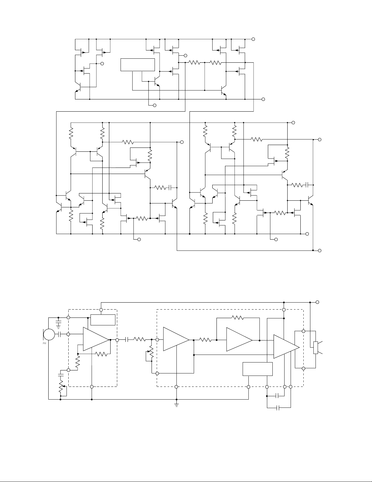
CIRCUIT DESCRIPTION
The GS551 is a 10 pin, low voltage, class B amplifier which
operates over a battery range of 1.1 VDC to 3 VDC.
The GS551 consists of three gain blocks. The first block is
an inverting amplifier with the gain set by two external
resistors. The gain trim feature can be used as a volume
control in hearing aid applications. The second block is an
inverting unity gain amplifier which serves as a phase
splitter. The outputs from the first and second blocks drive
the differential input of the third block. The third block has
a fixed AC gain of 28 dB when driving a receiver.
The amplifier has internal compensation eliminating the
need for a capacitor across the receiver. Two ground pins
are available for “Star” grounding to reduce any second
order harmonic distortion introduced by ground line resistance.
V
B
6
10
C OUT 2
1
C OUT 1
3
A IN
A OUT
4
U.S. Patent No. 4,719,430
Other Patents Pending
5
- A
29
GND 1
- B
REFERENCE
VOLTAGE
GND 2
C
7
VREF DEC 1
8
DEC 2
BLOCK DIAGRAM
Revision Date: January 2001
GENNUM CORPORATION P.O. Box 489, Stn. A, Burlington, Ontario, Canada L7R 3Y3 tel. +1 (905) 632-2996
Web Site: www.gennum.com E-mail: hipinfo@gennum.com
Document No. 510 - 31 - 04

ABSOLUTE MAXIMUM RATINGS
PIN CONNECTION
PARAMETER VALUE/UNITS
Supply Voltage 5 VDC
Operating Temperature -10 to +40 °C
Storage Temperature -20 to +70 °C
CAUTION
A IN
A OUT
DEC 1
GND 1
C OUT 1
5
VB
6
VREF
DEC 2
GND 2
101
COUT 2
CLASS 1 ESD SENSITIVITY
ELECTRICAL CHARACTERISTICS
Conditions: Frequency = 1 kHz, Temperature = 25°C, Supply Voltage V
PARAMETER SYMBOL CONDITIONS MIN TYP MAX UNITS
= 1.3 VDC
B
Gain A
Amplifier Current I
Transducer Current I
V
AMP
TRANS
VO=0.707 VRMS 46 48 50 dB
120 220 335 µA
120 250 390 µA
Input Referred Noise IRN NFB 0.2 to 10 kHz at 12 dB/Oct - 1.3 2.5 µV
Total Harmonic Distortion VO=0.707 VRMS - 0.25 1.3 %
THD
VO=1.3 VRMS - 0.3 1.5 %
Stable with RB to R
Maximum Output Current I
All parameters remain as shown in Test Circuit unless otherwise stated in "Conditions" column
C
R
S
S
10k
0.1
STAB
OUT
5
- A
100k
RB=22Ω - - 22 Ω
VP8=0 - >35 - mA
= 1.3VDC
V
B
6
10
RB = 4.7
I
OUT
V
O
- B
C
RL = 400
510 - 31 - 04
1 kHz
4
All resistors in ohms,all capacitors in farads
unless otherwise stated
REFERENCE
VOLTAGE
1
29783
0.047
0.047
Fig. 1 Test Circuit
2
7
6
4
Base Current
Compensation
2
5
6
1
10
REGULATOR
+
_
4
0.1
30k
R
S
3.9k
3
4.7
2
0.1
230
1
1.0
R
GT
50k
All resistors in ohms,all capacitors in farads unless otherwise stated
5
8
Fig. 2 GS551 Functional Schematic
10k
R
VC
100k
5
- A
4
2
3
2
9
1.3 VDC
6
10
- B
REFERENCE
VOLTAGE
C
1
CI2960
GS551LC506
9783
0.047
0.047
Fig. 3 Application Circuit
3
510 - 31 - 04
10
0
-10
-20
-30
-40
-50
-60
OUTPUT (dBV)
-70
-80
-90
-130 -120 -110 -100 -90 -80 -70 -60 -50 -40 -30 -20 -10
RVC=100k
RVC=47k
RVC=22k
RVC=10k
RVC=3.3k
INPUT (dBV)
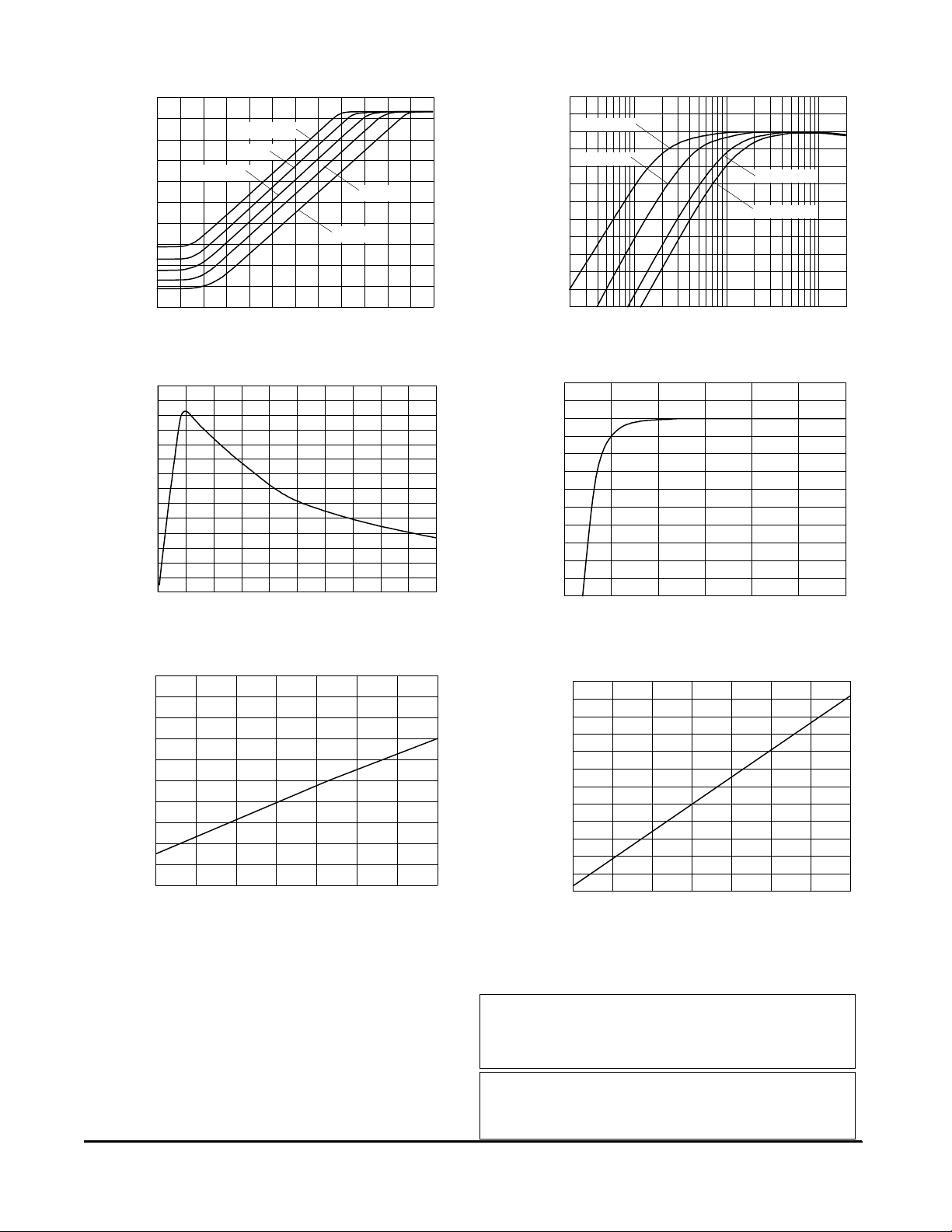
Fig. 4 I/O Characteristics at Various
Gain Settings (RS=3.92k)
14
13
12
11
10
9
8
7
6
5
4
3
POWER OUTPUT (mW)
2
1
0
0 100 200 300 400 500 600 700 800 900 1000
LOAD RESISTANCE (Ω)
Fig. 6 Power Outout vs Load Resistance
at 7% Distortion, RB=0Ω, VB=1.35V
0.10
0.08
0.06
0.04
0.02
0
-0.02
-0.04
RELATIVE GAIN (dB)
-0.06
-0.08
-0.10
-20 -10 0 10 20 30 40 50
TEMPERATURE (°C)
Fig. 8 Gain vs Temperature
4
2
CS=0.22 µF
0
-2
CS=0.1 µF
-4
-6
-8
-10
-12
-14
-16
RELATIVE OUTPUT (dB)
-18
-20
20 200 2k 20k
CS=0.047 µF
CS=0.033µF
FREQUENCY (Hz)
Fig. 5 Closed Loop Frequency Response
at Various CS Values (RS=3.92k)
10
5
0
-5
-10
-15
-20
-25
-30
-35
RELATIVE GAIN (dB)
-40
-45
-50
.8 .9 1 1.1 1.2 1.3 1.4
SUPPLY VOLTAGE (VDC)
Fig. 7 Gain vs Supply Voltage
50
40
30
20
10
0
-10
-20
-30
-40
-50
-60
RELATIVE AMPLIFIER CURRENT (µA)
-70
-20 -10 0 10 20 30 40 50
TEMPERATURE (°C)
Fig. 9 Amplifier Current vs Temperature
GENNUM CORPORATION
MAILING ADDRESS:
P.O. Box 489, Stn. A, Burlington, Ontario, Canada L7R 3Y3
Tel. +1 (905) 632-2996 Fax +1 (905) 632-2814
SHIPPING ADDRESS:
970 Fraser Drive, Burlington, Ontario, Canada L7L 5P5
GENNUM JAPAN CORPORATION
C-101, Miyamae Village, 2-10-42 Miyamae, Suginami-ku, Tokyo 168-0081,
DOCUMENT IDENTIFICATION: DATA SHEET
The product is in production. Gennum reserves the right to make
changes at any time to improve reliability, function or design, in
order to provide the best product possible.
REVISION NOTES:
Changes to standard packaging information.
Japan Tel. +81 (3) 3334-7700 Fax: +81 (3) 3247-8839
Gennum Corporation assumes no responsibility for the use of any circuits described herein and makes no representations that they are free from patent infringement.
510 - 31 - 04
© Copyright August 1988 Gennum Corporation. All rights reserved. Printed in Canada.
4
 Loading...