

Datasheet GS4981-ITA, GS4981-IKA, GS4981-IDA, GS4981-CTA, GS4981-CKA Datasheet (Gennum Corporation)
...
GS1881, GS4881, GS4981
Monolithic Video Sync Separators
DATA SHEET
FEATURES
• noise tolerant odd/even flag, back porch and
horizontal sync pulse
• fast recovery from impulse noise
• excellent temperature stability
• 0.5 V to 4 Vpp input signal amplitude with 5 V
supply
• well-controlled clamp discharge current and
slicing level
• programmable horizontal scan rate (up to 130 kHz)
• composite, vertical, back porch, odd/even
(GS1881, GS4881), horizontal (GS4981) outputs
• predictable vertical output pulse width with
default trigger for non-standard video signals
• 5 V to 12 V supply voltage range
• pin compatible with LM1881 sync separator
SELECTION CHART
APPLICATION CHOOSE DEVICE:
Direct LM1881 Replacement GS1881
with Improved Performance
New Applications GS4881
Substitution for LM1881
New Applications Requiring GS4981
Horizontal Sync Output
DESCRIPTION
The GS1881, GS4881 and GS4981 are general purpose sync
separators for use in a wide variety of video applications. The
devices extract the timing information from composite video
signals with scan rates from 15 to 130 kHz.
The GS1881 is a drop-in replacement for the industry standard
LM1881 with much improved performance. The device
generates composite sync, vertical sync, back porch and
odd/even field signals. The GS4881 is identical to the GS1881
but features a noise immune back porch pulse which maintains
a constant H rate during the vertical interval. The GS4981 is
identical to the GS4881, except that it provides horizontal sync
in place of the odd/even output.
All three devices feature a self-adjusting windowing circuit for
noise immunity, which synchronizes to H rate. This
windowing circuit determines the odd or even field
in the GS1881 and GS4881, gates the back porch pulse in
the GS4881 and GS4981, and generates the horizontal sync
output in the GS4981.
The devices feature an improved input stage which ensures
that the input signal is sliced at a predictable point due to
well-controlled input clamp discharge current and sync
slicing level. A missing pulse detector enables the devices to
recover quickly from impulse noise disturbances by temporarily
increasing the clamp discharge current by roughly ten times.
The input stage will operate with signals from 0.5 to 4 volts
peak to peak with a 5 volt supply.
The GS1881, GS4881 and GS4981 also feature a predictable
vertical output pulse width with a default trigger for non-standard
video signals. All three are available in commercial and
industrial temperature ranges and are packaged in both DIP
and SOIC.
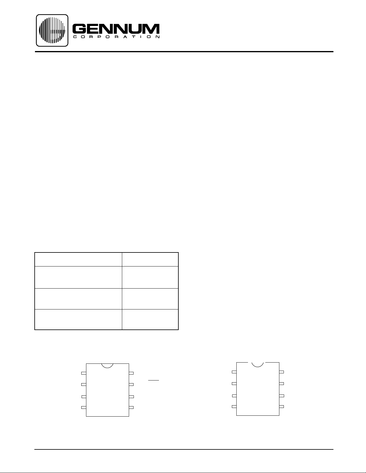
PIN CONNECTIONS
GS1881, GS4881
COMPOSITE
SYNC OUT
COMPOSITE
VIDEO IN
VERTICAL
SYNC OUT
GROUND
Patent No. 5,432,559
Revision Date: October 1995
GENNUM CORPORATION P.O. Box 489, Stn A, Burlington, Ontario, Canada L7R 3Y3 tel. (905) 632-2996 fax: (905) 632-2055
Japan Branch: A-302 Miyamae Village, 2-10-42 Miyamae, Suginami-ku, Tokyo 168, Japan tel. (03) 3247-8838 fax (03) 3247-8839
1
2
3
4
8 PIN DIP
8 PIN SOIC
8
7
6
5
V
cc
ODD/EVEN
R
SET
BACK PORCH
COMPOSITE
SYNC OUT
COMPOSITE
VIDEO IN
VERTICAL
SYNC OUT
GROUND
GS4981
1
2
3
4
8 PIN DIP
8 PIN SOIC
V
8
cc
HORIZONTAL
7
6
R
SET
5
BACK PORCH
Document No. 520 - 23 - 03
GS1881 ELECTRICAL CHARACTERISTICS
(VCC= 5 V, R
= 680 kΩ, TA = 25° C, unless otherwise specified)
SET
PARAMETER CONDITIONS MIN TYP MAX UNITS
Supply Voltage 4.5 5 13.2 V
Supply Current Outputs at Logic 1 V
V
= 5 V - 4.6 6.5 mA
CC
= 12 V - 5.0 7.0 mA
CC
Video Input (Pin 2)
(a) Signal Level V
= 5 V 0.5 - 4 Vp-p
CC
(b) Clamp Current Charge 500 650 850 µA
Discharge - normal 9 11 13 µA
- Nosync flag raised 65 95 115 µ A
(c) Delay to raising of Nosync flag Video input held high 64 95 130 µs
(d) Sync Tip Clamp Voltage - 1.55 - V
Sync Slice Level Relative to sync tip clamp voltage 70 77 84 mV
R
Pin Reference Voltage (Pin 6) See Note 1 1.14 1.24 1.34 V
SET
Composite Sync Out (Pin 1) See Note 2 40 60 80 ns
Delay from Video CL = 15p
Back Porch Pulse Out (Pin 5) CL = 15p
(a) Delay from Rising
Edge of Sync 400 500 650 ns
(b) Pulse Width 2.0 2.5 3.2 µs
Vertical Sync Out (Pin 3)
(a) Pulse Width Serrations during vertical interval 197.7 197.7 197.7 µs
(b) Default Starting Time No serrations during the vertical interval 48 65 82 µs
Horizontal Scan Rate Modified R
SET
15 - 130 kHz
Logic Outputs
(a) V
OH
I
= 40 µA VCC = 5 V 4.2 4.6 - V
OH
VCC = 12 V 11.2 11.6 - V
IOH = 1.6 mA VCC = 5 V 2.4 3.4 - V
VCC = 12 V 9.4 10.4 - V
(b) V
OL
IOL = -1.6 mA - 0.3 0.6 V
Note 1: When placing the R
as possible to pin 6. Care should also be taken to avoid parasitic capacitive coupling from any output pin (pins 1, 3, 5 and 7) to pin 6.
Note 2: Measured from slicing point of input falling edge to 50% point of composite sync falling edge.
resistor and the 0.1µF decoupling capacitor careful attention should be made to ensure that they are as close
SET
ORDERING INFORMATION
Part Number Package Type Temperature Range
GS1881 - CDA 8 PDIP 0° to 70° C
GS1881 - CKA 8 SOIC 0° to 70° C
GS1881 - CTA 8 TAPE 0° to 70° C
GS1881 - IDA 8 PDIP -25° to 85° C
GS1881 - IKA 8 SOIC -25° to 85° C
GS1881 - ITA 8 TAPE -25° to 85° C
520 - 23 - 03
2
CAUTION
ELECTROSTATIC
SENSITIVE DEVICES
DO NOT OPEN PACKAGES OR HANDLE
EXCEPT AT A STATIC-FREE WORKSTATION
GS4881 ELECTRICAL CHARACTERISTICS
(VCC= 5 V, R
= 680 kΩ, TA = 25° C, unless otherwise specified)
SET
PARAMETER CONDITIONS MIN TYP MAX UNITS
Supply Voltage 4.5 5 13.2 V
Supply Current Outputs at Logic 1 V
V
= 5 V - 4.6 6.5 mA
CC
= 12 V - 5.0 7.0 mA
CC
Video Input (Pin 2)
(a) Signal Level V
= 5 V 0.5 - 4 Vp-p
CC
(b) Clamp Current Charge 500 650 850 µA
Discharge - normal 9 11 13 µA
- Nosync flag raised 65 95 115 µA
(c) Delay to raising of Nosync flag Video input held high 64 95 130 µs
(d) Sync Tip Clamp Voltage - 1.55 - V
Sync Slice Level Relative to sync tip clamp voltage 70 77 84 mV
R
Pin Reference Voltage (Pin 6) See Note 1 1.14 1.24 1.34 V
SET
Composite Sync Out (Pin 1) See Note 2 40 60 80 ns
Delay from Video CL = 15p
Back Porch Pulse Out (Pin 5) CL = 15p
(a) Delay from Rising
Edge of Sync 400 500 650 ns
(b) Pulse Width 2.0 2.5 3.2 µs
(c) Occurence Rate H H H
Vertical Sync Out (Pin 3)
(a) Pulse Width Serrations during vertical interval 197.7 197.7 197.7 µs
(b) Default Starting Time No serrations during the vertical interval 48 65 82 µs
Horizontal Scan Rate Modified R
SET
15 - 130 kHz
Logic Outputs
(a) V
OH
I
= 40 µA VCC = 5 V 4.2 4.6 - V
OH
VCC = 12 V 11.2 11.6 - V
IOH = 1.6 mA VCC = 5 V 2.4 3.4 - V
VCC = 12 V 9.4 10.4 - V
(b) V
OL
IOL = -1.6 mA - 0.3 0.6 V
Note 1: When placing the R
as possible to pin 6. Care should also be taken to avoid parasitic capacitive coupling from any output pin (pins 1, 3, 5 and 7) to pin 6.
Note 2: Measured from slicing point of input falling edge to 50% point of composite sync falling edge.
resistor and the 0.1µF decoupling capacitor careful attention should be made to ensure that they are as close
SET
ORDERING INFORMATION
Part Number Package Type Temperature Range
GS4881 - CDA 8 PDIP 0° to 70° C
GS4881 - CKA 8 SOIC 0° to 70° C
GS4881 - CTA 8 TAPE 0° to 70° C
GS4881 - IDA 8 PDIP -25° to 85° C
GS4881 - IKA 8 SOIC -25° to 85° C
GS4881 - ITA 8 TAPE -25° to 85° C
3
520 - 23 - 03
GS4981 ELECTRICAL CHARACTERISTICS
(VCC= 5 V, R
= 680 kΩ, TA = 25° C, unless otherwise specified)
SET
PARAMETER CONDITIONS MIN TYP MAX UNITS
Supply Voltage 4.5 5 13.2 V
Supply Current Outputs at Logic 1 V
V
= 5 V - 4.6 6.5 mA
CC
= 12 V - 5.0 7.0 mA
CC
Video Input (Pin 2)
(a) Signal Level V
= 5 V 0.5 - 4 Vp-p
CC
(b) Clamp Current Charge 500 650 850 µA
Discharge - normal 9 11 13 µA
- Nosync flag raised 65 95 115 µA
(c) Delay to raising of Nosync flag Video input held high 64 95 130 µs
(d) Sync Tip Clamp Voltage - 1.55 - V
Sync Slice Level Relative to sync tip clamp voltage 70 77 84 mV
R
Pin Reference Voltage (Pin 6) See Note 1 1.14 1.24 1.34 V
SET
Composite Sync Out (Pin 1) See Note 2 40 60 80 ns
Delay from Video CL = 15p
Back Porch Pulse Out (Pin 5) CL = 15p
(a) Delay from Rising
Edge of Sync 400 500 650 ns
(b) Pulse Width 2.0 2.5 3.2 µs
(c) Occurence Rate H H H
Vertical Sync Out (Pin 3)
(a) Pulse Width Serrations during vertical interval 197.7 197.7 197.7 µs
(b) Default Starting Time No serrations during the vertical interval 48 65 82 µs
Horizontal Sync Out (Pin 7) CL = 15p
(a) Delay from Video 90 190 290 ns
(b) Pulse Width 5.0 7.0 9.0 µs
Horizontal Scan Rate Modified R
SET
15 - 130 kHz
Logic Outputs
(a) V
OH
I
= 40 µA VCC = 5 V 4.2 4.6 - V
OH
VCC = 12 V 11.2 11.6 - V
IOH = 1.6 mA VCC = 5 V 2.4 3.4 - V
Note 3 VCC = 12 V 9.4 10.4 - V
(b) V
OL
Note 1: When placing the R
as possible to pin 6. Care should also be taken to avoid parasitic capacitive coupling from any output pin (pins 1, 3, 5 and 7) to pin 6.
Note 2: Measured from slicing point of input falling edge to 50% point of composite sync falling edge.
Note 3: Applies only to composite sync, vertical sync, and back porch outputs. Horizontal sync has a passive 10 kΩ pull-up to V
resistor and the 0.1µF decoupling capacitor careful attention should be made to ensure that they are as close
SET
IOL = -1.6 mA - 0.3 0.6 V
.
CC
ORDERING INFORMATION
Part Number Package Type Temperature Range
GS4981 - CDA 8 PDIP 0° to 70° C
GS4981 - CKA 8 SOIC 0° to 70° C
GS4981 - CTA 8 TAPE 0° to 70° C
GS4981 - IDA 8 PDIP -25° to 85° C
GS4981 - IKA 8 SOIC -25° to 85° C
GS4981 - ITA 8 TAPE -25° to 85° C
520 - 23 - 03
4
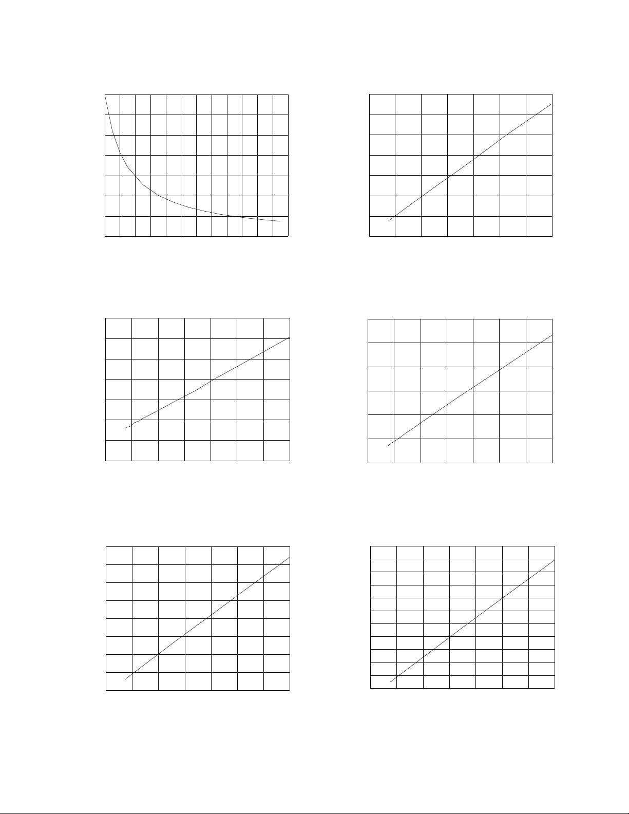
TYPICAL PERFORMANCE CHARACTERISTICS (VS = 5V, TA = 25° C unless otherwise shown)
700
600
500
400
(kΩ)
SET
R
300
200
100
0
15 35 55 75 95 115 135
SCAN RATE (kHz)
Fig. 1 R
700
600
500
400
300
200
vs Scan Rate
SET
BACK PORCH DELAY (ns)
100
70
60
50
40
30
20
VERTICAL DEFAULT TIME (µs)
10
0
0 100 200 300 400 500 600 700
R
(kΩ)
SET
Fig. 2 Vertical Sync Default Starting Time
vs R
SET
3000
2500
2000
1500
1000
BACK PORCH WIDTH (ns)
500
0
0 100 200 300 400 500 600 700
R
(kΩ)
SET
Fig. 3 Back Porch Delay vs R
8000
7000
6000
5000
4000
3000
HORIZONTAL WIDTH (µs)
2000
1000
0
0 100 200 300 400 500 600 700
R
(kΩ)
SET
Fig. 5 Horizontal Width vs R
SET
SET
0
0 100 200 300 400 500 600 700
R
(kΩ)
SET
Fig. 4 Back Porch Width vs R
110
100
90
80
70
60
50
40
30
NOSYNC DELAY TIME (µs)
20
10
0
0 100 200 300 400 500 600 700
R
(kΩ)
SET
Fig. 6 Nosync Delay Time vs R
SET
SET
5
520 - 23 - 03
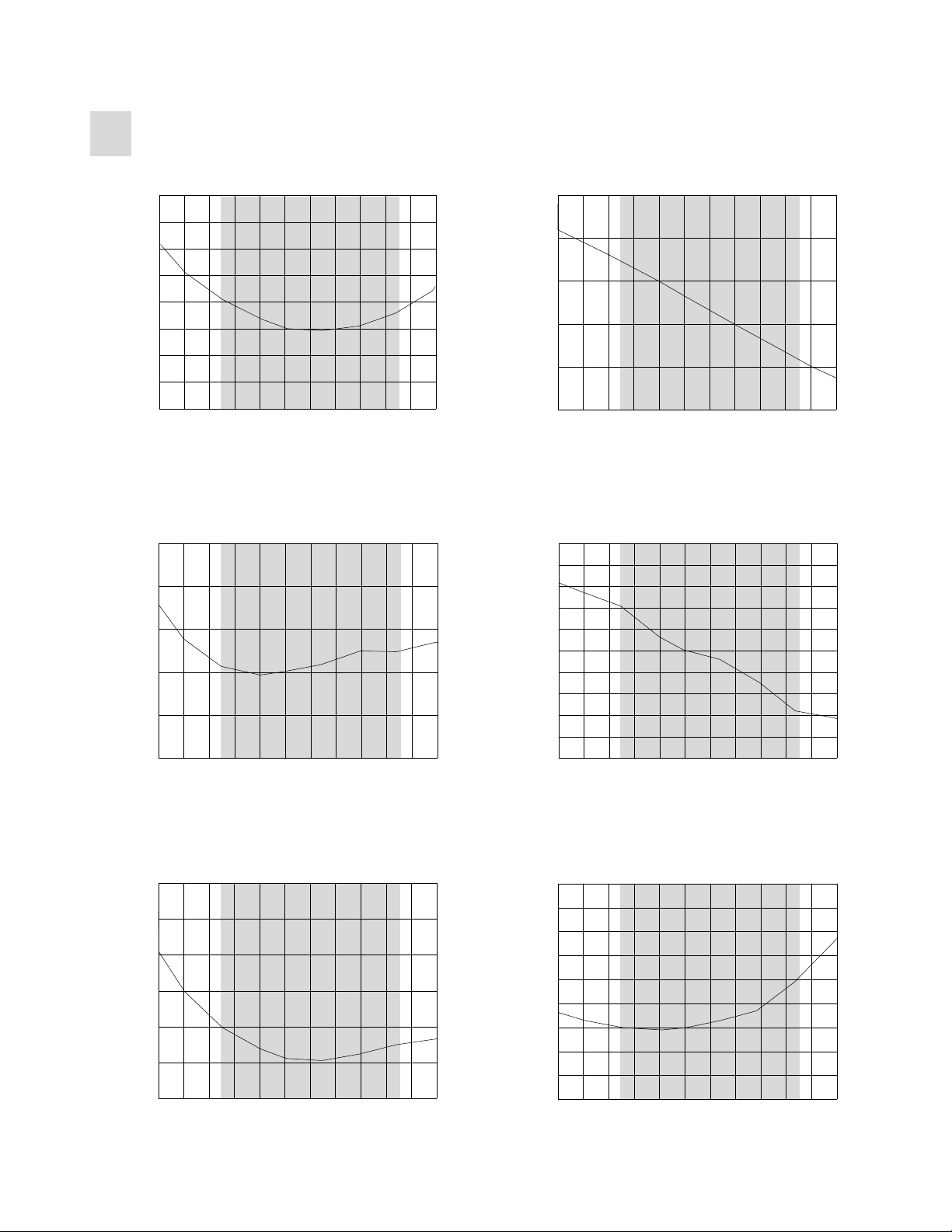
TEMPERATURE CHARACTERISTICS (V
Commercial Temperature Range (0 - 70 °C)
= 5V, R
S
= 680 kΩ unless otherwise shown)
SET
10
8
6
4
2
0
-2
COMPOSITE SYNC DELAY
VARIATION (ns)
-4
-6
-25 -15 -5 5 15 25 35 45 55 65 75 85
TEMPERATURE (°C)
Fig. 7 Composite Sync Delay Variation
vs Temperature
30
20
10
0
-10
BACK PORCH DELAY VARIATION (ns)
-20
-25 -15 -5 5 15 25 35 45 55 65 75 85
TEMPERATURE (°C)
Fig. 9 Back Porch Delay Variation
vs Temperature
850
740
650
550
450
CLAMPING CURRENT (µA)
350
-25 -15 -5 5 15 25 35 45 55 65 75 85
TEMPERATURE (°C)
Fig. 8 Clamping Current vs Temperature
125
100
75
50
25
0
-25
-50
-75
100
BACK PORCH WIDTH VARIATION (ns)
-125
-25 -15 -5 5 15 25 35 45 55 65 75 85
TEMPERATURE (°C)
Fig. 10 Back Porch Width Variation
vs Temperature
25
20
15
10
5
0
HORIZONTAL DELAY VARIATION (ns)
-5
-25 -15 -5 5 15 25 35 45 55 65 75 85
Fig. 11 Horizontal Delay Variation
520 - 23 - 03
TEMPERATURE (°C)
vs Temperature
600
500
400
300
200
100
0
-100
-200
HORIZONTAL WIDTH VARIATION (ns)
-300
-25 -15 -5 5 15 25 35 45 55 65 75 85
6
TEMPERATURE (°C)
Fig. 12 Horizontal Width Variation
vs Temperature
CIRCUIT DESPCRIPTION
BACK PORCH OUTPUT (pin 5)
The block diagrams for the GS1881, GS4881 and GS4981,
are shown in Figures 17 through 19, with timing diagrams for
the devices shown in Figure 20.
When stimulated by a composite input signal, the GS1881
and GS4881 sync separators output composite sync,
vertical sync, back porch, and odd/even field information.
The GS4981 substitutes the odd/even output of the GS4881
with a horizontal output. An external resistor on pin 6 is used
to define internal currents allowing the devices to accommodate
horizontal scan rates from 15 kHz to 130 kHz.
COMPOSITE VIDEO INPUT (pin 2) and COMPOSITE
SYNC OUTPUT (pin 1)
Composite video is AC coupled via an external coupling
capacitor to pin 2. The device clamps the sync tip of the input
video to 1.5 V ( V
clamp voltage ( V
) and then slices at 77 mV above the
clamp
). The resultant signal, provided at
slice
pin 1, is a reproduction of the input signal with the active video
portion removed. As V
clamp
and V
are supply and input
slice
signal independent, for 0.5 V p-p signals (sync height of 143
mV) slicing will occur at just above the 50% point and for 2 V
p-p signals (sync height of 572 mV) slicing will occur at
approximately 13% of sync height.
The video signal path and composite sync slicing circuitry
have been optimized and compensated to achieve a low
propagation delay that is stable over temperature. The typical
delay is 60 ns with less than 3 ns drift over the commercial
temperature range.
In an NTSC composite video signal, horizontal sync pulses are
followed by the back porch interval. The device generates a
negative going pulse on pin 5 during this time. It is delayed
typically 500 ns from the rising edge of sync and has a typical
width of 2.5 µs. Both of these times are set by the external R
SET
resistor.
During the pre-equalizing, vertical sync, and post-equalizing
periods, composite sync doubles in frequency. The GS4881
and GS4981 maintain the back porch output at the horizontal
rate due to Back Porch Enable (BPEN), generated by the
internal windowing circuit, which forces back porch to be
asserted at the horizontal rate. This gating circuit is also the
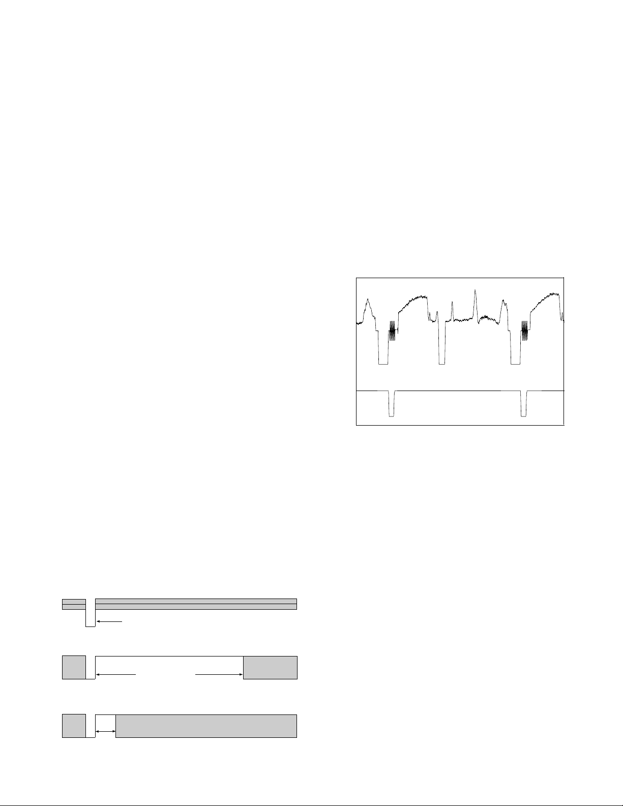
reason for the excellent impulse noise immunity of the back
porch output as shown in Figure 14.
Video
Input
Impulse
Noise
Back
Porch
Output
GS4881
GS4981
Fig. 14 Back Porch Noise Immunity
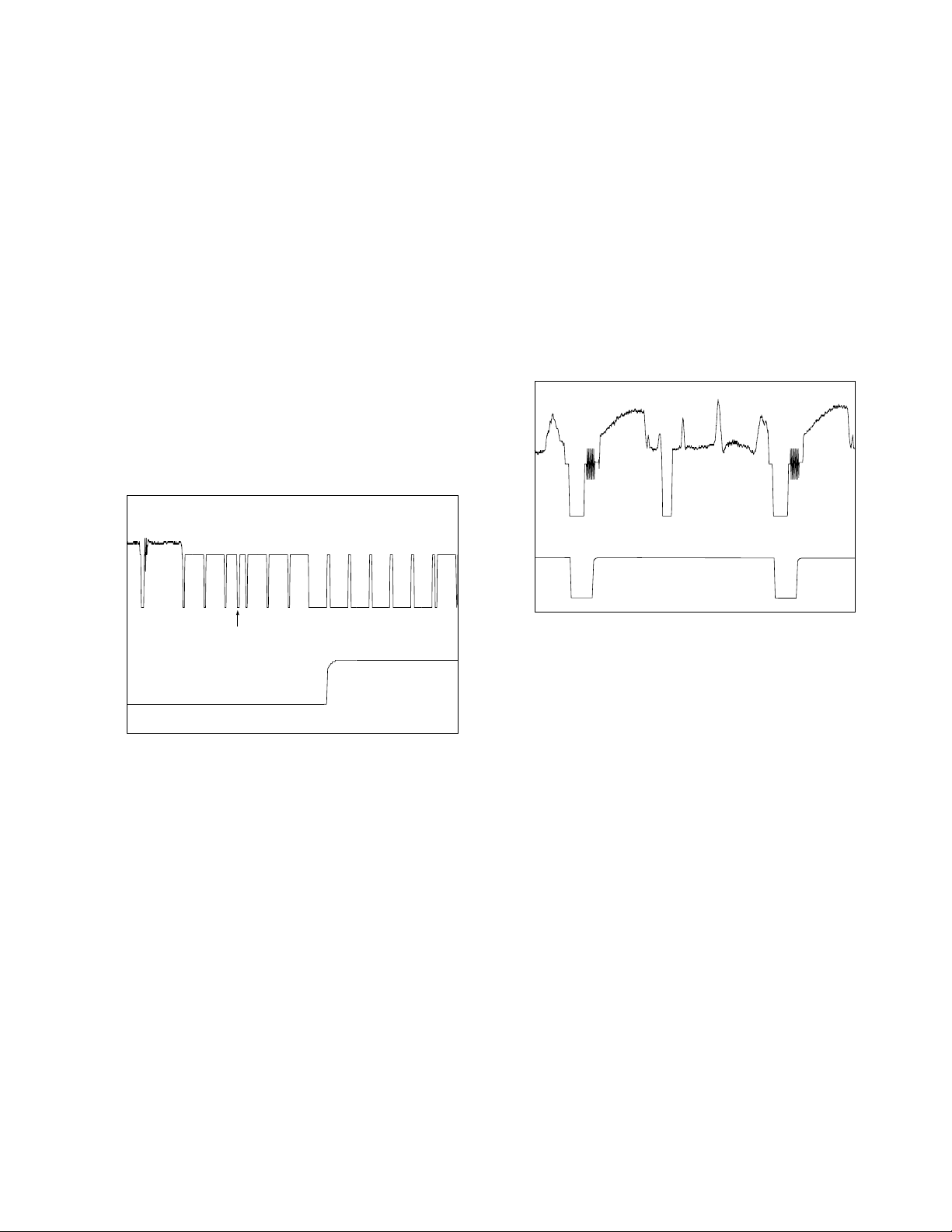
The typical input clamp discharge current is 11µA. This
current is optimal under normal operating circumstances but
needs to be increased when the clamp is trying to recover
from negative going impulse noise. The device improves the
recovery time by raising a NOSYNC flag when there has not
been a sync pulse for approximately 1
1
/2 horizontal lines.
When this flag is raised the discharge current is increased by
85 µA so that the recovery time is sped up by nearly 10 times.
Figure 13 shows a comparison between the recovery times
with and without the increased discharge current.
VIDEO INPUT
IMPULSE NOISE
COMPOSITE SYNC RECOVERY TIME without INCREASED DISCHARGE CURRENT (LM1881)
RECOVERY TIME T1
COMPOSITE SYNC RECOVERY TIME with INCREASED DISCHARGE CURRENT (GS1881, GS4881, GS4981)
RECOVERY TIME
T1 / 10
Fig. 13 Impulse Noise: Recovery Time Comparison
The GS1881 does not gate the Back Porch which allows for
total pin compatibility with the LM1881.
VERTICAL SYNC OUTPUT (pin 3)
The vertical sync interval is detected by integrating the
composite sync pulses. The first broad vertical sync pulse
causes an internal capacitor to charge past a fixed threshold
and raises an internal vertical flag. Once the vertical flag is
raised, the positive edge of the next serration clocks out the
vertical output. When the vertical sync interval ends, the first
post equalizing pulse is unable to charge the capacitor
sufficiently, causing the internal vertical flag to go high. The
rising edge of the second post-equalizing pulse then clocks
out the high flag to end the vertical sync pulse. The vertical
output is clocked in and out and therefore is a fixed width of
197.7 µs (3H + 4.7 µs + 2.3 µs). In the case of a non-standard
vertical interval that has no serrations, a second internal
capacitor is charged and clocks the vertical pulse out after
typically 65 µs. In this case the end of the vertical pulse will still
be the rising edge of the second post-equalizing pulse. As the
vertical detector is designed as a true integrator, it provides
improved noise immunity.
7
520 - 23 - 03
ODD/EVEN FIELD OUTPUT (pin 7 GS1881, GS4881)
HORIZONTAL OUTPUT (pin 7 GS4981)
NTSC PAL and SECAM composite video standards are
interlaced video schemes and therefore have odd and even
fields. For odd fields the first broad vertical sync pulse is
coincident with the start of horizontal, while for even fields the
first broad vertical sync pulse starts in the middle of a horizontal
line. Therefore by comparing the vertical sync with an internally
generated horizontal sync the odd/even field information is
determined. This output is clocked out by the falling edge of
vertical sync. The odd/even output is low during even fields
and high during odd fields. This method of detecting odd and
even fields is very noise tolerant.
Noise during the pre-equalizing pulses does not affect the
output since the field decision is made at the beginning of the
vertical interval. This noise immunity is displayed in Figure 15
in which an extra pre-equalizing pulse has been added to the
video input with no negative effect on the odd/even field
information.
Video
Input
As mentioned above, the odd/even field output of the
GS1881 and GS4881 is generated by comparing vertical
sync with an internal horizontal sync signal. This horizontal
sync signal is a true horizontal signal (i.e. maintained during
the vertical interval) and is outputted on pin 7 for the
GS4981. A delay of 190 ns from the video input and a width
of 6.5 µs are typically characteristics for this signal.
The windowing circuit which generates horizontal provides
excellent impulse noise immunity as shown in Figure 16. This
output buffer is an open collector stage with an internal
10 kΩ pull up resistor.
Video
Input
Impulse
Noise
Horizontal
Output
Odd/Even
Output
Impulse
Noise
Even Odd
Fig. 15 Odd/Even Output
Fig. 16 Horizontal Output
520 - 23 - 03
8
VIDEO
INPUT
(Pin 2)
11µ
V
(Pin 8)
R_SET
(Pin 6)
C SYNC
-
-
V SLICE
+
V CLAMP
+
-
HORIZONTAL
+
WINDOWING
CIRCUIT
Q
D
Q
G
D
CLK
Q
Q
COMPOSITE
SYNC OUTPUT
(Pin 1)
ODD / EVEN
OUTPUT
(Pin 7)
85µ
NOSYNC
CC
VOLTAGE
REGULATOR
VERTICAL
DETECTOR
D
CLK
Q
Q
1.2V
BACK PORCH
TIMING
CURRENTS
DETECTOR
VERTICAL SYNC
OUTPUT
(PIN 3)
BACK PORCH
OUTPUT
(Pin 5)
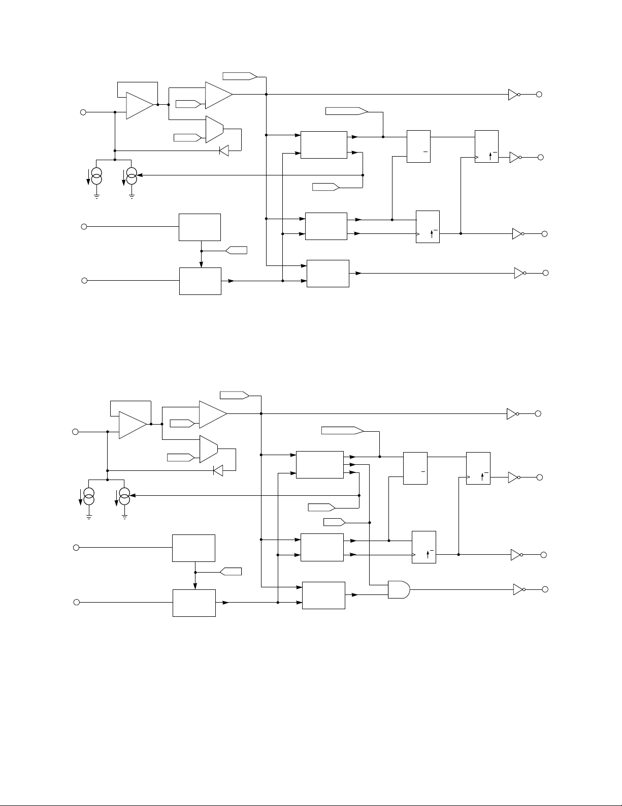
Fig. 17 GS1881 Block Diagram
VIDEO
INPUT
(Pin 2)
11µ
V
(Pin 8)
R_SET
(Pin 6)
C SYNC
-
-
+
V CLAMP
V SLICE
+
-
HORIZONTAL
+
WINDOWING
CIRCUIT
D
Q
Q
G
D
CLK
Q
Q
COMPOSITE
SYNC OUTPUT
(Pin 1)
ODD / EVEN
OUTPUT
(Pin 7)
85µ
NOSYNC
B PEN
CC
VOLTAGE
REGULATOR
VERTICAL
DETECTOR
D
CLK
Q
Q
1.2V
BACK PORCH
TIMING
CURRENTS
DETECTOR
VERTICAL SYNC
OUTPUT
(PIN 3)
BACK PORCH
OUTPUT
(Pin 5)
Fig. 18 GS4881 Block Diagram
9
520 - 23 - 03

VIDEO
INPUT
(Pin 2)
C SYNC
-
+
-
+
V 1
-
+
V 2
WINDOWING
10k
CIRCUIT
COMPOSITE
SYNC OUTPUT
(Pin 1)
HORIZONTAL
OUTPUT
(Pin 7)
11µ
V
(Pin 8)
R_SET
(Pin 6)
COMPOSITE SYNC OUTPUT
GS1881, GS4881, GS4981
BACK PORCH OUTPUT
85µ
CC
COMPOSITE
VIDEO INPUT
GS4881, GS4981
NOSYNC
B PEN
D
CLK
Q
Q
VOLTAGE
REGULATOR
VERTICAL
DETECTOR
1.2V
BACK PORCH
TIMING
CURRENTS
DETECTOR
Fig. 19 GS4981 Block Diagram
525 1 2 3 4 5 6 7 8
VERTICAL SYNC
OUTPUT
(PIN 3)
BACK PORCH
OUTPUT
(Pin 5)
BACK PORCH OUTPUT
HORIZONTAL OUTPUT
VERTICAL SYNC OUTPUT
GS1881, GS4881, GS4981
GS1881
GS4981
ODD/EVEN OUTPUT
GS1881, GS4881
600ns
2.5µs
COMPOSITE
VIDEO INPUT
BACK PORCH
OUTPUT
500ns
2.5µs
Fig. 20 GS1881, GS4881, GS4981 Video Sync Separator Timing Diagram
520 - 23 - 03
10
APPLICATION NOTES
(1) Choosing the Appropriate Input Coupling Capacitor to
Optimize Slicing Level and Hum Rejection
The video designer can adjust the slicing level by choosing the
value of the input coupling capacitor. The relationship between
slicing level and input coupling capacitor is described by the
following equation.
I
∆V
where: I
∆T = T
C
SLICE
DIS
= ∆T = V
C
C
= clamp discharge current = 11 µA
DIS
- T
LINE
= input coupling capacitor
C
DROOP
= (63.5 µs - 4.7 µs)
SYNC
Figure 21 is a graphical representation of this equation and
photographs 1 and 2 show the input video waveforms
for 0.1 µF and 0.01 µF input capacitors respectively. The
advantage in choosing a smaller input coupling capacitor, is
increased hum rejection as the following analyses illustrates.
137
127
117
107
97
SLICING LEVEL (mV)
87
77
0.01 0.02 0.03 0.04 0.05 0.06 0.07 0.08 0.09 0.10
Fig. 21 Slicing Level vs Input Coupling Capacitor
CH1
INPUT COUPLING CAPACITOR (µF)
VIDEO
VIDEO
CH1
CH2
0.1µF
75Ω
Test Circuit 1
CH1
0.01µF
75Ω
CH2
8
2
6
4
680k
0.1µ
CH2
Photograph 1
CH1
8
2
6
4
680k
0.1µ
CH2
Test Circuit 2
11
Photograph 2
520 - 23 - 03

The interfering hum component is defined by:
verifying that there is enough clamping current
v
where: V
ƒ
HUM
HUM
(t) = V
cos(2πƒ
P
= Peak voltage of AC hum
P
HUM
t)
= Frequency of hum (50 Hz or 60 Hz)
The maximum rate of change of this hum signal occurs at the
zero crossing points and is:
dv
HUM
= ± V
dt
t =
π 3π
,
2 2
P
2πƒ
HUM
Since the horizontal scan period is much faster than the period
of the interference ( 63.5 µs << 1/ƒ
is to assume that the maximum line to line voltage change
) a good approximation
HUM
resulting from the interfering hum is:
∆V
where: T
The total line to line voltage change (∆V
by adding the hum component (∆V
component (V
∆V
DROOP
T
= ± VP2πƒ
HUM
= 63.5 µs
LINE
). This calculation results in two cases:
T
HUM
LINE
) can then be calculated
T
) and the droop
HUM
∆V
T
Case A Case B
∆VT = ∆V
To correct for ∆V
in case A, the input stage must be able to
T
charge the input capacitor ∆V
+ V
HUM
DROOP
volts in 4.7 µs. This is not a
T
constraint as the typical clamping current of 650 µA can
accomplish this for practical values of coupling capacitor.
The only way to compensate for ∆VT in case B is to make
V
DROOP
> ∆ V
HUM
. V
is increased by decreasing the input
DROOP
coupling capacitor value. Therefore the video designer can
increase hum rejection by decreasing the value of this capacitor.
The following is a numerical example:
∆V
= 29.4 mV + 29.4 mV = 58.8 mV
t
.
. i = 0.022 µ = 275 µA
.
58.8 mV
( )
4.7 µ
which is less than 650 µA.
(2) FIltering
In order to keep the input to output delay small and temperature
stable, no chrominance filtering is done within the device.
External filtering may be necessary if the input signal contains
large chrominance components (less than 77 mV from sync
tip) or has significant amounts of high frequency noise. This
filter can be a simple low pass RC network constructed by a
resistance (R
to ground. A single pole low pass filter having a corner
) in series with the source and a capacitor (Cƒ)
S
frequency of approximately 500 kHz will provide ample
bandwidth for passing sync pulses with almost 18 dB
attenuation at 3.58 MHz. Care should be taken in choosing
the value of the series resistor in the filter since the source
resistance seen by the sync separator affects its performance.
As the source resistance rises, the video input sync tip starts
to be clipped due to the clamping current during the sync.
This clamping current is relatively large due to the
non-symmetric duty cycle of video. To a good approximation
the amount of sync clamp current can be calculated as
follows:
I
( I
CLAMP
CLAMP
.
) (T
AVG
(4.7 µs) = (11 µA) (63. 5 µs - 4.7 µs)
AVG
.
. I
CLAMP
) = (I
SYNC
AVG
DIS
= 137.6 µA
) (T
LINE
- T
SYNC
)
This clamp current flows in the source resistance causing a
voltage drop equal to :
V
= ( I
CLIP
CLAMP
= (137.6 µ) (R
AVG
) (RS)
)
S
... V
choosing C
= (63.5 µ - 4.7 µ) = 29.4 mV
DROOP
11
0.022
= 0.022 µF
c
the maximum amount of 60 Hz hum that could be rejected
would be when:
∆V
... VP = = =1.23v
520 - 23 - 03
DROOP
= ∆V
∆V
DROOP
2
πƒ
HUMTLINE
= V
HUM
2πƒ
P
29.4mV
2π(60) (63.5 µ)
HUM TLINE
PEAK
HUM
12
VIDEO
INPUT
I
CLAMP
R
S
- +
V
CLIP
75Ω
Fig. 22 Simple Chrominance Filtering
CC
C
ƒ
2
4
8
6
680k
0.1µ
Photograph 3 shows the amount of sync clipping for a 560 Ω
source resistor. A graph of V
Figure 23, and Figure 24 shows the corresponding capacitor
versus RS is shown in
CLIP
value for a particular series resistor to provide a corner
frequency of 500 kHz.
In applications where signal levels are small the amount of
attenuation should be minimized. It follows from Figure 23 and
Figure 24 that in order to minimize attenuation a small series
resistor and a larger capacitor to ground should be chosen.
This however, increases the capacitive loading of the signal
source.
Another way to minimize the amount of attenuation is to control
the source resistance seen by the sync separator by using a
PNP emitter follower (Figure 25). A PNP emitter follower works
well to drive the sync separator, and does not require much
DC current because the transistor provides the current when
it is needed during sync. Figure 26 is a typical application
circuit that minimizes sync tip clipping.
CH1
CH1
VIDEO
560Ω
75Ω
CH2
8
2
0.1µF
6
4
Test Circuit 3
100
90
80
70
60
(mV)
50
CLIP
40
V
30
20
10
0
0 100 200 300 400 500 600 700
SERIES RESISTOR (Ω)
Fig. 23 V
vs Series Resistor
CLIP
680k
0.1µ
CH2
Photograph 3
10
9
8
7
6
5
Cƒ (nF)
4
3
2
1
0
0 100 200 300 400 500 600 700
SERIES RESISTOR (Ω)
Fig. 24 Cƒ vs Series Resistor
VIDEO
INPUT
V
CC
5.6k
2
C
4
75Ω
FILTER
C
-5V
Fig. 25 PNP Emitter Follower Buffer
V
CC
-5V
5.6k
CC
8
2
6
4
680k
0.1µ
8
6
680k
0.1µ
VIDEO
INPUT
75Ω
5.6k
56p
Fig. 26 Typical NTSC Application Circuit
13
520 - 23 - 03
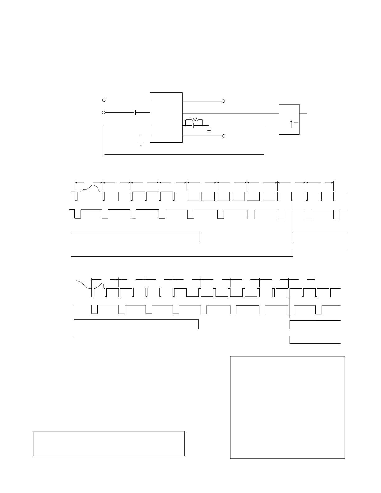
(3) Deriving Odd/Even Using the GS4981
Odd/even field information can be derived using the vertical
and horizontal outputs from the GS4981 along with an external
positive edge D flip/flop. The horizontal output is used
as the D input and the vertical output as the clock, as
shown in Figure 27.
GS4981
1
2
3
4
Fig. 27 Derivation of Odd/Even with GS4981
START OF ODD FIELD
COMPOSITE
VIDEO INPUT
HORIZONTAL OUTPUT
VERTICAL SYNC OUTPUT
GS4981
GS4981
COMPOSITE
SYNC OUTPUT
COMPOSITE
VIDEO INPUT
VERTICAL
SYNC OUTPUT
525 1 2 3 4 5 6 7 8
0.1µF
At the start of an odd field the vertical output ends in the middle
of the horizontal line and a high will be latched. At the start of
an even field, the vertical output ends near the beginning of
the horizontal line and since the horizontal output is low, a low
will be latched. This timing sequence is shown in Figure 28.
5 - 12V
V
8
7
680kΩ
6
0.1µF
5
CC
HORIZONTAL
R
SET
BACK PORCH
OUTPUT
D FLIP/FLOP
D Q
CLK Q
V
ODD/EVEN
OUTPUT
ODD/EVEN OUTPUT
START OF EVEN FIELD
263 264 265 266 267 268 269 270
COMPOSITE
VIDEO INPUT
HORIZONTAL
GS4981
VERTICAL SYNC OUTPUT
GS4981
ODD/EVEN OUTPUT
REVISION NOTES
The only change from 520-23-02 to 520-23-03 is that the document has been
upgraded to a full DATA SHEET. It is no longer Preliminary.
Fig. 28 Timing Diagram
DOCUMENT
IDENTIFICATION
PRODUCT PROPOSAL
This data has been compiled for market investigation purposes
only, and does not constitute an offer for sale.
ADVANCE INFORMATION NOTE
This product is in development phase and specifications are
subject to change without notice. Gennum reserves the right to
remove the product at any time. Listing the product does not
constitute an offer for sale.
PRELIMINARY
The product is in a preproduction phase and specifications are
subject to change without notice.
DATA SHEET
The product is in production. Gennum reserves the right to
make changes at any time to improve reliability, function or
design, in order to provide the best product possible.
Gennum Corporation assumes no responsibility for the use of any circuits described herein and makes no representations that they are free from patent infringement.
520 - 23 - 03
© Copyright March 1991 Gennum Corporation. All rights reserved. Printed in Canada.
14
 Loading...