

Page 1
FEATURES
• SMPTE 292M compliant
• dual cable driving outputs optimized for driving data
up to 1.485Gb/s
• ±7% tolerance output
• >17dB output return loss
• minimum external components
• seamless interface with the HD-LINX™ family of
products
•low power
• standard packaging
APPLICATIONS
1.485Gb/s HDTV Serial Digital Receiver Interfaces for:
Routers, Distribution Amplifiers, Switchers, and other
transmitting equipment.
™
HD-LINX
GS1508
HDTV Cable Driver
PRELIMINARY DATA SHEET
DESCRIPTION
The GS1508 is a first generation very high speed bipolar
integrated circuit designed to drive two 75Ω co-axial
cables. The GS1508 is a SMPTE 292M compliant cable
driver that directly interfaces with other Gennum HDTV
devices and can also be used as a general purpose high
speed cable driver.
The GS1508 features two complementary outputs whose
amplitude is controlled within a precise ±7% variation. The
output amplitude can be varied by adjusting the R
resistor value.
The serial inputs can be AC coupled. The GS1508 is a low
power device that does not require external pull down
resistors. The GS1508 is packaged in an 8 pin SOIC and
operates from a single 5V power supply.
ORDERING INFORMATION
SET
GS1508
SDI
SDI
PART NUMBER PACKAGE TEMPERATURE
GS1508-CKA 8 pin SOIC 0°C to 70°C
GS1508-CTA 8 pin Tape and Reel 0°C to 70°C
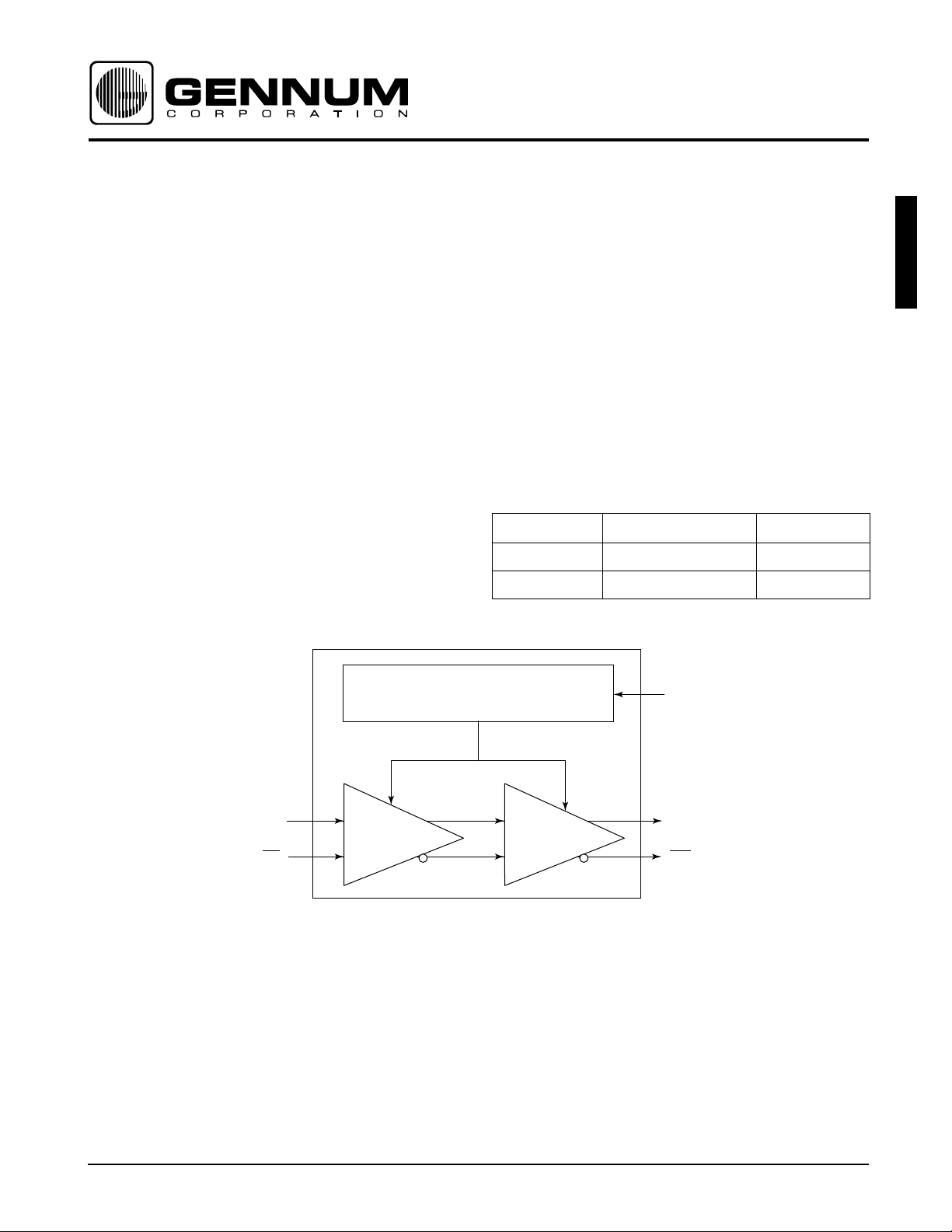
BANDGAP REFERENCE AND BIASING CIRCUIT
INPUT
DIFFERENTIAL
PAIR
PATENT PENDING
OUTPUT STAGE &
CONTROL
R
SET
SDO
SDO
BLOCK DIAGRAM
Revision Date: March 2000 Document No. 522 - 02 - 03
GENNUM CORPORATION P.O. Box 489, Stn. A, Burlington, Ontario, Canada L7R 3Y3
Tel. +1 (905) 632-2996 Fax. +1 (905) 632-5946 E-mail: info@gennum.com
www.gennum.com
Page 2
ABSOLUTE MAXIMUM RATINGS
TA = 25°C unless otherwise indicated
PARAMETER VALUE
Supply Voltage 5.5V
Input Voltage Range (any input) -0.3 to (V
+0.3)V
CC
Operating Temperature Range 0°C to 70°C
Storage Temperature -65°C to 150°C
Power Dissipation 300mW
Lead Temperature (soldering, 10 sec) 260°C
GS1508
Input ESD Voltage 2000V
DC ELECTRICAL CHARACTERISTICS
VCC = 5V, TA = 0°C to 70°C unless otherwise shown.
Specifications assume 800mV output amplitude level settings into end terminated 75Ω transmission lines. Data Rate = 1485Mb/s unless otherwise shown.
PARAMETER CONDITIONS SYMBOL MIN TYP MAX UNITS NOTES
Supply Voltage V
System Power
Consumption
Driving two
75Ω cables
Supply Current
Common Mode Input
V
CC
P
D
I
S
CM,IN
4.75 5.00 5.25 V 1
- 215 265 mW 1
-4354mA 1
2.5+(V
)-V
DIFF/2
-(V
CC
)V 2
DIFF/2
Voltage Range
Common Mode Output
V
CM,OUT
-V
CC-VOUT
-V 2
Voltage Range
AC ELECTRICAL CHARACTERISTICS
VCC = 5V, TA = 0°C to 70°C unless otherwise shown.
Specifications assume 800mV output amplitude levels into end terminated 75Ω transmission lines. Data Rate = 1485Mb/s unless otherwise shown.
PARAMETER CONDITIONS SYMBOL MIN TYP MAX UNITS NOTES
Serial Digital Rate DC 1485 - Mb/s 1
Additive Jitter 1485Mb/s - 5 - ps
Differential Input V
Differential Output V
DIFF
OUT
150 - 800 mV diff p-p 2
750 800 850 mV p-p 1
RMS
13
TEST
LEVEL
TEST
LEVEL
Output Rise/Fall Times (20% - 80%) t
Mismatch in Output Rise/Fall
, t
R
F
- 120 250 ps 2 1
-1530ps 4
Times
Overshoot - 1 8 % 4
Duty Cycle Distortion - 15 30 ps 1
Output Return Loss 5MHz to 1485MHz - 17 - dB 2 4
NOTES:
1. RMS additive jitter measured using Pseudo Random bit sequence (2
2. Measured with Gennum Evaluation Board (EB1508).
23
- 1).
TEST LEVELS:
1. 100% tested at 25°C.
2. Guaranteed by design.
3. Correlated Value.
4. Tested with EB1508
2
522 - 02 - 03
Page 3
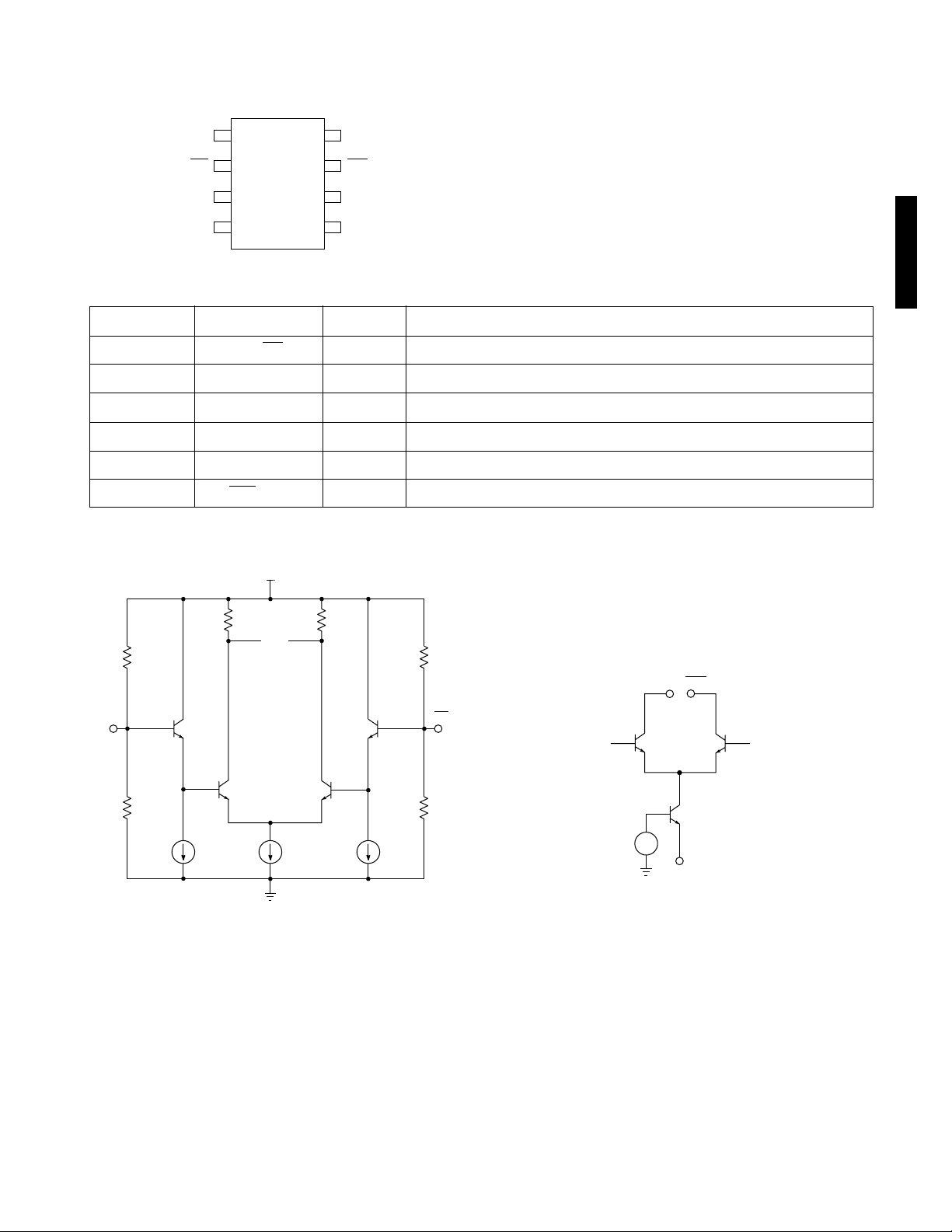
PIN CONNECTIONS
R
SET
SDO
SDO
+
-
TOP
8
SDO
7
SDO
6
GND
5
V
CC
R
SDI
SDI
V
SET
EE
1
2
GS1508
3
VIEW
4
PIN DESCRIPTIONS
NUMBER SYMBOL TYPE DESCRIPTION
1, 2 SDI, SDI
3V
4R
5V
EE
SET
CC
I Serial data inputs (non-inverting and inverting).
P Most negative supply voltage.
I Output amplitude control resistor.
P Most positive supply voltage.
6 GND P Not connected internally. Connect to Ground. Used for isolation.
7, 8 SDO
, SDO O Serial data outputs (non-inverting and inverting).
INPUT / OUTPUT CIRCUITS
V
CC
GS1508
SDI
5k
SDI
20k
Fig. 1 (Pins 1 and 2) Fig. 2 (Pins 7 and 8)
3
522 - 02 - 03
Page 4

DETAILED DESCRIPTION
INPUT INTERFACING
SDI/SDI are high impedance differential inputs. (
Figure 1 for equivalent input circuit
).
Several conditions must be observed when interfacing to
these inputs:
1. The differential input signal amplitude must be between
150 and 800mVpp.
GS1508
2. The common mode voltage range must be as specified
in the DC Characteristics table. For a 400mV input from
the GS1504 HD cable equalizer, this corresponds to a
common mode voltage range of between 2.7 and 4.8
volts.
3. For input trace lengths longer than approximately 1cm,
the inputs should be terminated as shown in the Typical
Application Circuit.
The GS1508 inputs are self biased, allowing for simple AC
coupling to the device. For serial digital HDTV, a minimum
capacitor value of 4.7µF should be used to allow coupling
of pathological test signals. A tantalum capacitor is
recommended.
OUTPUT INTERFACING
The GS1508 outputs are current mode, and will drive
800mV into a 75 ohm load. These outputs are protected
from accidental static damage with internal static protection
diodes.
See
Fig. 3 Output Optimized for Waveform Symmetry
L=8.2nH, R=75 (Typical ORL=13.5dB)
The SMPTE 292M standard requires that the output of a
cable driver have a source impedance of 75Ω and a return
loss of at least 15dB between 5Mhz and 1.485GHz.
In order for an HD SDI output circuit using the GS1508 to
meet this specification, the output circuit shown in the
Typical Application Circuit is recommended.
The values of L
COMP
and C
will vary depending on PCB
COMP
layout, but typical values are 12nH and 0.5pF respectively.
The small value of C
can be easily swamped by
COMP
parasitic PCB capacitance, so it is recommended that the
ground plane be removed under the GS1508 output
circuitry (
sheet for further details
see the Application Information section in this data
). A 4.7µF capacitor is used for AC
coupling the output of the GS1508. This value is chosen to
ensure that pathological signals can be coupled without a
significant DC component occurring.
Fig. 4 Output Optimized for Return Loss
L=12nH, C=0.5pF, R=75 (Typical ORL=18dB)
Figures 3 and 4 show the eye diagram of the GS1508
output for two different output compensation conditions.
Figure 4 shows the GS1508 output optimized for wideband
return loss of 18dB. Figure 3 shows the GS1508 output
optimized for output waveform symmetry. In this case the
output may not exhibit a return loss of 15dB.
When measuring return loss at the GS1508 output it is
necessary to take the measurement for both a logic high
and a logic low output condition. This is because the output
protection diodes act as a varactor (voltage controlled
capacitor) as shown in Figure 5.
Consequently, the output capacitance of the GS1508 is
dependent on the logic state of the output.
522 - 02 - 03
4
Page 5

GS1508
1.000
SDO
SDO
Fig. 5 Static Protection Diodes
OUTPUT RETURN LOSS MEASUREMENT
To perform a practical return loss measurement, it is
necessary to force the GS1508 output to a DC high or low
condition. The actual measured return loss will be based on
the outputs being static at V
or VCC-1.6V. Under normal
CC
operating conditions the outputs of the GS1508 swing
between V
-0.4V and VCC-1.2V, so the measured value of
CC
return loss will not represent the actual operating return
loss.
A simple method of calculating the values of actual
operating return loss is to interpolate the two return loss
measurements. In this way, the values of return loss are
estimated at V
measurements at V
-0.4V and VCC-1.2V based on the
CC
and VCC-1.6V.
CC
The two values of return loss (high and low) will typically
differ by several decibels. If the measured return loss is R
for logic high and RL for logic low, then the two values can
be interpolated as follows:
0.800
0.600
0.400
OUTPUT SWING
0.200
0.000
0.0000 0.0050 0.0100 0.0150 0.0200 0.0250
1 / R
(mho)
SET
Fig. 6 GS1508 Output Amplitude vs. 1/R
TABLE 1: R
vs V
SET
OUT
R
R 1/R
SET
SET
OUTPUT SWING
500.0 0.0020 0.095
150.0 0.0067 0.298
75.0 0.0133 0.575
53.6 0.0187 0.785
43.2 0.0231 0.937
NOTE: For reliable operation of the GS1508 over the full
temperature range, do not use an R
H
value below 49.9Ω.
SET
SET
GS1508
= RH- (RH-RL)/4 and
R
IH
R
= RL+(RH-RL)/4
IL
where R
is the interpolated logic high value and RIL is the
IH
interpolated logic low value.
For example, if R
interpolated values are R
OUTPUT AMPLITUDE ADJUSTMENT
= -18dB and RL = -14dB, then the
H
= -17dB and RIL = -15dB.
IH
The output amplitude of the GS1508 can be adjusted by
changing the value of the R
and Table 1. For an 800mV
resistor as shown in Figure 6
SET
output with a nominal ±7%
p-p
tolerance, a value of 53.6% is required. A ±1% SMT resistor
should be used.
The R
resistor is part of the high speed output circuit of
SET
the GS1508. The resistor should be placed as close as
possible to the R
pin. In addition, PCB capacitance
SET
should be minimized at this node by removing the PCB
groundplane beneath the R
resistor and the R
SET
SET
pin.
5
522 - 02 - 03
Page 6

TYPICAL APPLICATION CIRCUIT
PECL INPUT
Z
Z
0
0
GS1508
1n
TABLE 2: Typical Application Circuit Component Values
COMPONENT VALUE COMMENT
53.6
V
CC
100n
75
1
SDI
2
SDI
GS1508
3
V
EE
4
R
SET
SDO
SDO
GND
V
CC
8
7
6
5
0µ1
75
V
CC
All resistors in ohms,
all capacitors in farads,
unless otherwise shown.
C
COMP
L
COMP
L
COMP
C
COMP
75
75
4µ7
+
+
4µ7
OUT
OUT
R
L
C
SET
Z
0
COMP
COMP
53.6 For 800mV Output
50
Ω
For 50Ω PCB trace impedance
12nH Typical value. Component value will vary depending on PCB layout.
0.5pF Typical value. Component value will vary depending on PCB layout.
APPLICATION INFORMATION
PCB LAYOUT
Special attention must be paid to component layout when
designing serial digital interfaces for HDTV. Figures 8
through 11 show the artwork for a four layer printed circuit
evaluation board for the GS1508. The schematic is shown in
Figure 7. An FR-4 dielectric can be used, however,
controlled impedance transmission lines are required for
PCB traces longer than approximately 1cm. Note the
following PCB artwork features used to optimize
performance:
PCB trace width for HD rate signals is closely matched to
SMT component width to minimize reflections due to
change in trace impedance
The PCB ground plane is removed under the GS1508
output components to minimize parasitic capacitance.
The PCB ground plane is removed under the GS1508 R
SET
pin and resistor to minimize parasitic capacitance
Input and output BNC connectors are surface mounted inline to eliminate a transmission line stub caused by a BNC
mounting via High speed traces are curved to minimize
impedance changes due to change of PCB trace width.
522 - 02 - 03
6
Page 7

GS1508 EVALUATION BOARD
J7
EDGEMNT_BNC
J6
EDGEMNT_BNC
All resistors in ohms,
all capacitors in farads,
unless otherwise shown.
C14
1µ
C13
1µ
V
CC
1µ
C1
100n
C2
1n
C3
V
CC
R8
75
R7
75
C15
10n
C10
100n
V
TP2
L2 10n
R9
75
C17 0p5
L3 10n
CC
C18
R10
75
0p5
R12
TP1
C16
1n
50
R13
R11
53.6
50
SDI
SDI
V
R
EE
SET
U2
SDO
SDO
GND
V
CC
Fig. 7 Schematic Diagram for the GS1508 Evaluation Board
C11
4µ7
EDGEMNT_BNC
C12
4µ7
EDGEMNT_BNC
GS1508
J4
J5
Fig. 8 Top Layer of EB1508 PCB Layout
Fig. 9 Power Layer of EB1508 PCB Layout
Fig. 10 Ground Layer of EB1508 PCB Layout
Fig. 11 Bottom Layer of EB1508 PCB Layout
7
522 - 02 - 03
Page 8

PACKAGE DIMENSIONS
5.00 MAX.
0.49 MAX
1.91
MAX
1.27 MAX
8
1
GS1508
5
4.0
6.20
MAX
MAX
0.25
MAX
4
0.25
MAX
=
=
3.81
±0.05
3 spaces
=
±0.05
8-pin SOIC
All dimensions are in millimetres
0.60 MAX
@ 1.27
CAUTION
ELECTROSTATIC
SENSITIVE DEVICES
DO NOT OPEN PACKAGES OR HANDLE
EXCEPT AT A STATIC-FREE WORKSTATION
DOCUMENT IDENTIFICATION
PRELIMINARY DATA SHEET
This product is in production. Gennum reserves the right to make
changes to the product and to the documentation.
GENNUM CORPORATION
MAILING ADDRESS:
P.O. Box 489, Stn. A, Burlington, Ontario, Canada L7R 3Y3
Tel. +1 (905) 632-2996 Fax. +1 (905) 632-5946
SHIPPING ADDRESS:
970 Fraser Drive, Burlington, Ontario, Canada L7L 5P5
Gennum Corporation assumes no responsibility for the use of any circuits described herein and makes no representations that they are free from patent infringement.
522 - 02 - 03
REVISION NOTES:
Updated ordering information; Replaced evaluation board diagrams;
Updated pin descriptions; Added note to Table 1.
For the latest product information, visit www.gennum.com
GENNUM JAPAN CORPORATION
C-101, Miyamae Village, 2-10-42 Miyamae, Suginami-ku
Tokyo 168-0081, Japan
Tel. +81 (03) 3334-7700 Fax. +81 (03) 3247-8839
GENNUM UK LIMITED
25 Long Garden Walk, Farnham, Surrey, England GU9 7HX
Tel. +44 (0)1252 747 000 Fax +44 (0)1252 726 523
© Copyright August 1998 Gennum Corporation. All rights reserved. Printed in Canada.
8
 Loading...