

Page 1
1
Preliminary GR8837C
J: DIP-8
C: SOT-26
GR8837C
Package Code
RoHS Code
G: Green (Halogen Free) Device
L: PB Free Device
GR8837C
X X XXX
Serial No.
Code 1
Code 2
Code 1
37C X
X
X X X
Serial No.
Code 2
Year
2008
2009
2010
2011
2016
2017
2018
2019
Month
Jan.
Feb.
Mar.
Apr.
Sep.
Oct.
Nov.
Dec.
Green-Mode PWM Controller with Protection
Features
Current Mode Control
Standby Power below 100mW
Under-Voltage Lockout (UVLO)
Non-Audible-Noise Green-Mode Control
65KHz Switching Frequency
Internal Leading-Edge Blanking
Internal Slope Compensation
Internal Soft Start
Gate Output Voltage Clamp
Jitter and Soft Driving for Reducing EMI
Over-Load Protection (OLP)-Auto Recovery
Mode
Vcc OVP Protection- Auto Recovery Mode
300mA Driving Capability
Description
The GR8837C is a highly-integrated, low startup
current, current mode PWM controller with
green-mode function. The integr ated functions also
include the leading-edge blanking of the current
sensing, internal slope compensation, soft start
OLP, and OVP.These functions enable the power
supply to easily meet even the strictest power
requirements.
The GR8837C improves the performance and
reduces the cost of po wer supplies. It is with 8-pin
DIP and 6-pin SOT-26 package
O
Application
Switching AC/DC Adapter
Open Frame SMPS
Battery Charger
Ordering and Marking Information
DIP-8
SOT-26
Code 1 8 9 A B
Code 2 1 2 3 4 9 A B C
Grenergy OPTO Inc. reserves the right to make changes to improve reliability or manufacture ability without notice, and
advise customers to obtain the latest version of relevant information to verify before placing orders.
● ● ●
G H I J
2012.02 Ver. F .Copyright Grenergy OPTO, Inc. www.grenergy-ic.com
Page 2
2
Preliminary GR8837C
GND
COMP
BNO
OUT
VCC
CS
1
2
3 4
5
6
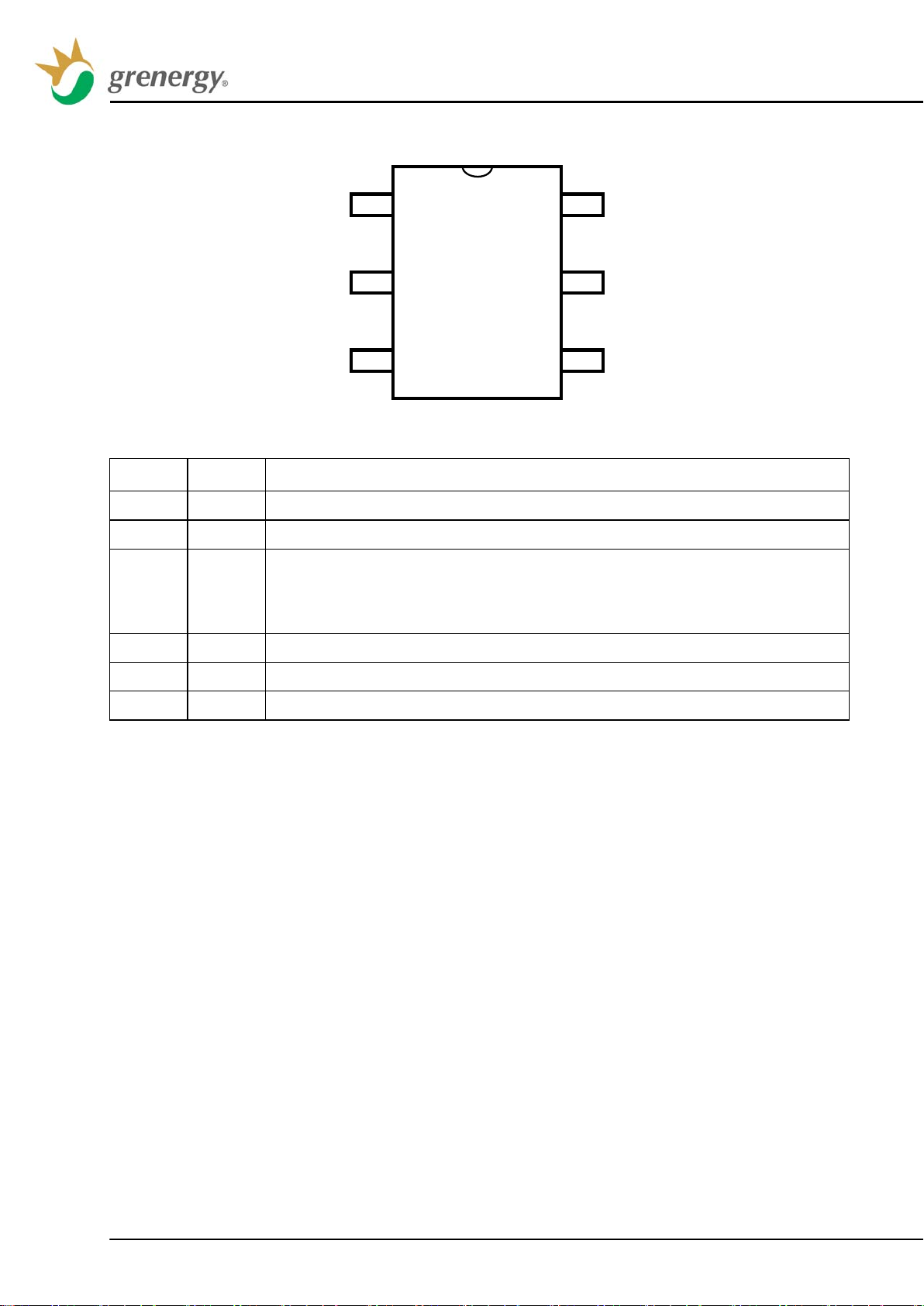
Pin Configuration
Pin Description
Pin No. Name Function
1 GND Ground pin
2 COMP Voltage feedback pin, by connecting a photo-coupler to control the duty cycle
Brownout protection pin. Connect a resistor divider between this pin and bulk
3 BNO
4 CS Current sense pin, connect to sense the MOSFET current
5 VCC Power supply pin
6 OUT The output driver for driving the external MOSFET
capacitor voltage to set the brownout level. If the voltage is less than threshold
voltage, the PWM output will be disabled
Absolute Maximum Ratings
Supply voltage VCC --------------------------------------------------------------------------------------------------------- 30V
COMP, BNO, CS ---------------------------------------------------------------------------------------------------- -0.3 ~ 7V
OUT ----------------------------------------------------------------------------------------------------------- -0.3 ~ VCC + 0.3V
Junction temperature ------------------------------------------------------------------------------------------------------- 150℃
Operating ambient temperature ------------------------------------------------------------------------------ -20℃ ~ 85℃
Storage temperature range ---------------------------------------------------------------------------------- -65℃ ~ 150 ℃
SOT-26 package thermal resistance (junction to ambient) -------------------------------------------------- 250℃/W
Power dissipation (SOT-26, at ambient temperature = 85℃) ------------------------------------------------ 250mW
Power dissipation (DIP-8, at ambient temperature = 85℃) --------------------------------------------------- 650mW
Lead temperature (All Pb free packages, soldering, 10 sec) -------------------------------------------------- 260℃
ESD voltage protection, human body model -------------------------------------------------------------------------- 2KV
ESD voltage protection, machine model ------------------------------------------------------------------------------ 200V
2012.02 Ver. F .Copyright Grenergy OPTO, Inc. www.grenergy-ic.com
Page 3
3
Preliminary GR8837C
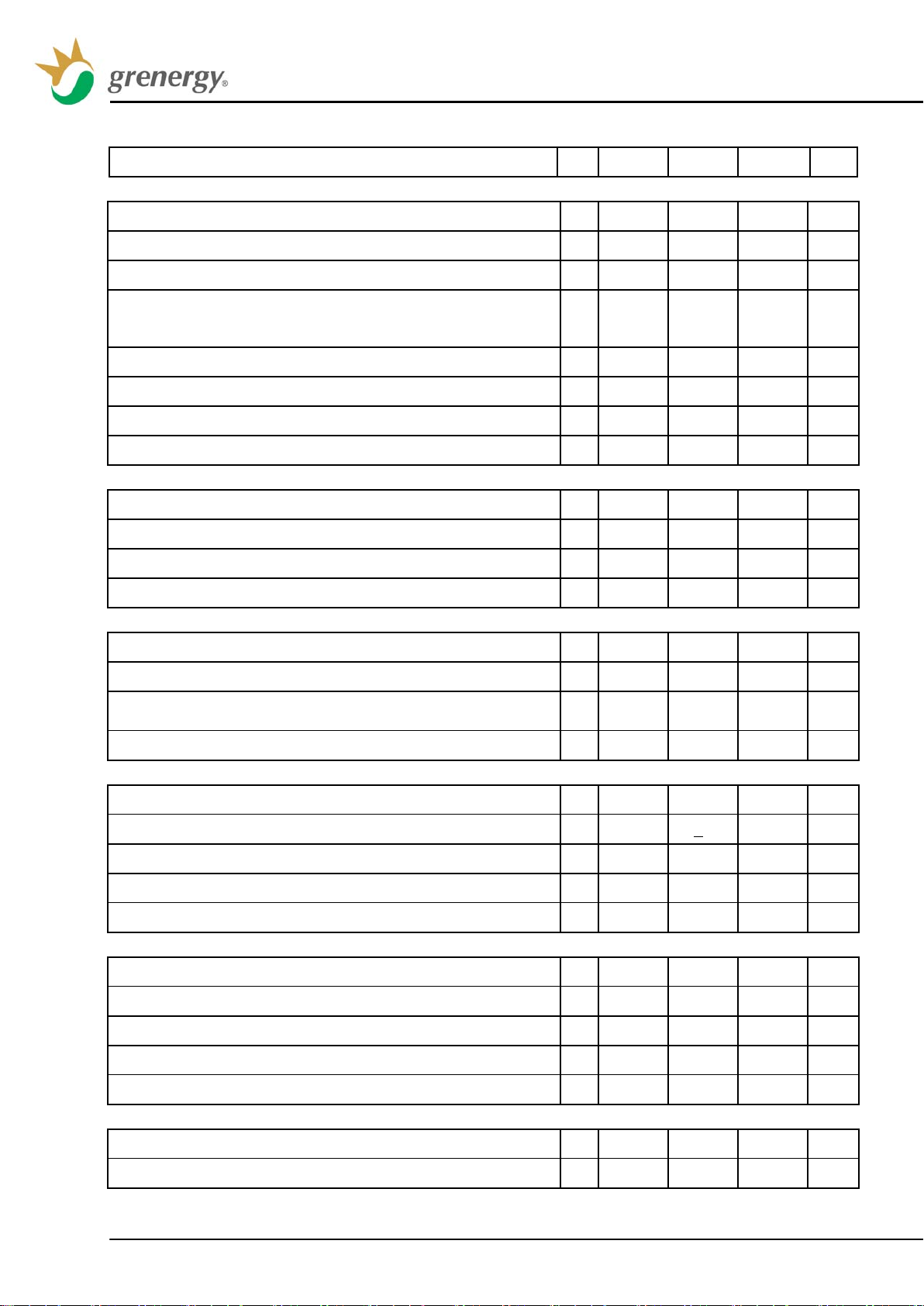
Electrical Characteristics (VCC = 15.0V & TA = +25℃,unless otherwise specified.)
Parameter Pin Min. Typ. Max. Unit
SUPPLY VOLTAGE
Startup Current (VCC=UVLO on - 1V) 5 8 15 uA
Operating Current (with 1nF load on OUT pin), Vcom p = 0V 5 800 uA
Operating Current (with 1nF load on OUT pin), Vcomp = 2.5V 5 2 mA
Operating Current (with 1nF load on OUT pin), Protection
Tripped (OLP, OVP)
UVLO(off) 5 5.8 6.8 7.8 V
UVLO(on) 5 10.3 11.3 12.3 V
OVP Level on VCC Pin- Auto Recovery Mode 5 27 28 29 V
VCC Level in Latch Mode (3Meg start-up resistor) 5 6 V
VOLTAGE FEEDBACK
Short Circuit Current, Vcomp = 0V 2 0.8 mA
Open Loop Voltage, COMP Pin Open 2 4.4 5.5 V
Green-Mode Start Voltage 2 1.5 V
Burst Mode Start Voltage 2 0.85 V
CURRENT SENSING
Maximum Input Voltage, Vcs(off)-Auto Recover y Mode 4 0.80 0.85 0.9 V
Leading-Edge Blanking Time 4 350 nS
Input Impedance 4 1
Delay to Output 4 100 nS
5 0.7 mA
mΩ
OSCILLATOR
Frequency - 60 65 70 KHz
Jitter Frequency - +6 %
Green Mode Frequency - 20 22 25 KHz
Temp. Stability (-40°C ~ 110°C)
Voltage Stability (VCC = 11V~25V) - 3 %
GATE DRIVER OUTPUT
Output Low Level, VCC = 15V, Io = 20mA 6 1 V
Output High Level, VCC = 15V, Io = 20mA 6 8 V
Rising Time, Load Capacitance = 1000pF 6 200 nS
Falling Time, Load Capacitance = 1000pF 6 80 nS
VGATE-Clamp (VCC = 25V ) 6 13 V
OLP SECTION
OLP Trip Level, Vcomp (OLP) - 3.5 V
OLP Delay Time - 60 mS
2012.02 Ver. F .Copyright Grenergy OPTO, Inc. www.grenergy-ic.com
- 5 %
Page 4

4
Preliminary GR8837C
PWM SECTION
Maximum Duty Cycle - 70 75 80 %
Brownout Function
Brownout Turn-On Trip Level 1.1 V
Brownout Turn-Off Trip Level 0.8 V
2012.02 Ver. F .Copyright Grenergy OPTO, Inc. www.grenergy-ic.com
Page 5
5
Preliminary GR8837C
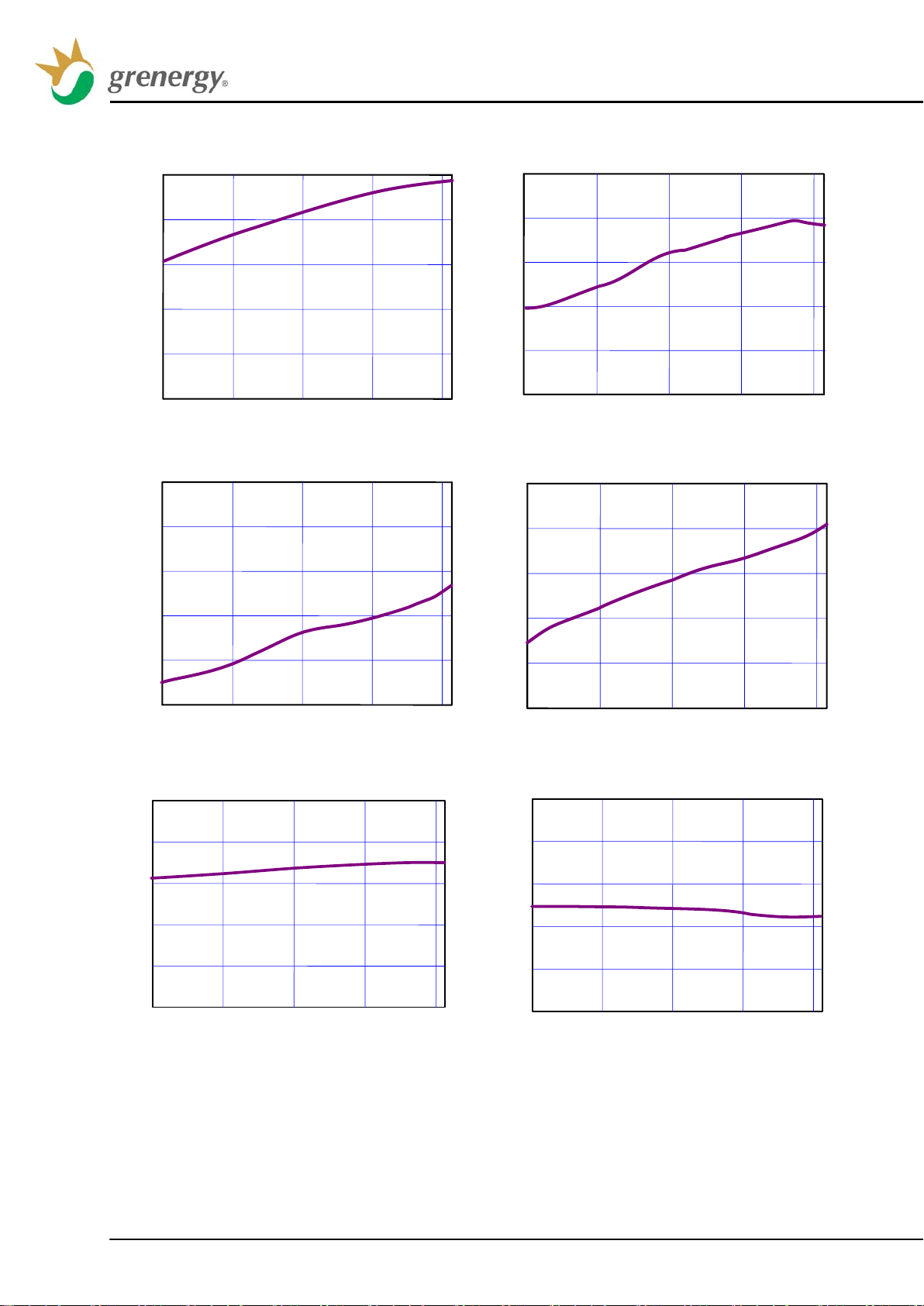
UVLO (on) (V)
Fig. 1 UVLO (on) vs. Temperature
10.3
10.4
10.5
10.6
10.7
10.8
-40
0
40
80
120 125
Temperature (℃)
Temperature (℃)
6.5
6.7
6.8
7.0
6.6
-40
0
40
80
120 125
6.9
UVLO (off) (V)
Fig. 2 UVLO (off) vs. Temperature
VDD Start up current (uA)
Fig. 3 VDD Start up current vs. Temperature
2.0
4.0
6.0
8.0
10.0
12.0
-40
0
40
80
120 125
Temperature (℃)
Operating current (mA)
Fig. 4
Operating current vs. Temperature
1.2
1.4
1.6
1.8
2.0
2.2
-40
0
40
80
120
125
Temperature (℃)
OLP-Trip Level (V)
Fig. 5 OLP Trip Level vs. Temperature
-
-40
0
40
80
120 125
3.0
3.2
3.4
3.6
3.8
4.0
Temperature (℃)
Maximum Input Voltage of CS pin(V)
Fig. 6 Maximum Input Voltage of CS pin vs. Temperature
-40
0
40
80
120 125
0.85
0.86
0.87
0.88
0.89
0.90
Temperature (℃)
Typical Performance Characteristics
2012.02 Ver. F .Copyright Grenergy OPTO, Inc. www.grenergy-ic.com
Page 6

6
Preliminary GR8837C
Frequency (KHz)
Fig. 7
Frequency
vs. Temperature
-40
0
40
80
120 125
63
64
65
66
67
68
Temperature (℃)
Green Mode Frequency (KHz)
Fig. 8
Green Mode Frequency vs.
Temperature
-40
0
40
80
120 125
20
21
22
23
24
2
5
Temperature (℃)
2012.02 Ver. F .Copyright Grenergy OPTO, Inc. www.grenergy-ic.com
Page 7

7
Preliminary GR8837C
UVLO (on) 11.3V
UVLO (off) 6.8V
Vcc
VCC
UVLO
(on)
UVLO
(off)
t
t
COMP
OLP
3.5 V
t
OUT
OLP delay time
Switching SwitchingNon - Switching
OLP trip Level
(
off
)
OLP Counter Reset
Application Information
Start-up Curr ent
The typical start-up current is around 8uA. Very low
start-up current allows the PWM controller to
increase the value of start-up resistor and then
frequency of the controller will decrease so as to
reduce the system power consumption. The
minimum frequency is about 22 KHz, which is
outside the audio range
.
reduce the power dissipation on it.
UVLO (Under Voltage Lockout)
A hysteresis UVLO comparator is implemented in
GR8837C, then the turn-o n and turn-off thresholds
level are fixed at 11.3V and 6.8V respectively. This
hysteresis shown in Fig.9 ensures that the start-up
capacitor will be adequate to supply the ch ip during
start-up. The GR8837C is designed to meet the
standby power below 100mW. So the start-up
resistor can be used as several Mega Ohms to
reduce the power loss. Due to the low UVLO on
level, so the turn-on delay time will also never
greater than the general PWM IC.
LEB (Leading-Edge Blanking)
Each time the power MOSFET is switched on, a
turn-on spike will inevitably occur at the sense
resistor. To avoid fault tr igger, a 350ns leading-edge
blanking time is built in. Conventional RC filtering
can therefore be omitted. During this blanking
period, the current-limit comparator is disabled and
can not switch off the gate driver.
Internal Slope Compensation
A bu i lt -in slope compensation circuit is c onstructed
in GR8837C. When the switch is on, a r amp voltage
is added to the sensed voltage acros s the CS pin,
which helps to stabilize the system and preve nt the
sub-harmonic oscillations
.
OLP (Over Load Protection)
The GR8837C has over load protection function. An
Fig.9
Soft Start
During initial power on, the GR8837C provides
16ms soft start function. It effectively suppresses
the start up peak current to reduce the power
MOSFET drain voltage especially at high line.
Oscillator
The maximum duty-cycle of internal oscillator is
limited to 75% for avoiding the transformer
saturation. The freque nc y of the osc illator is fixed to
65KHz by internal setting.
Green-Mode Operation
When the load decreases to an extent, the
2012.02 Ver. F .Copyright Grenergy OPTO, Inc. www.grenergy-ic.com
internal circuit detects the load level, when the load
is larger than a threshold level and the condition
lasts more than 60ms, the gate output will keep on
low level. Then VCC decreases below UVLO off
level, the controller resets again. Fig.10 shows the
waveform of the OLP operation.
Fig. 10
Page 8

8
Preliminary GR8837C
VCC
UVLO(off)
t
t
LOAD
t
OUT
Switching
VCC mode(on)
VCC mode(off)
Full load
VCC mode
Burst mode
VCC
UVLO(on)
UVLO(off)
t
OVP Tripped
t
OUT
Switching
Switching
Non-Switching
OVP Level
OVP (Over Voltage Pr o tection) on VCC
To prevent power MOSFET from being damaged,
the GR8837C is implem ented an OVP function on
VCC. When the VCC voltage is higher than the OVP
threshold voltage, the outp ut gate driver circuit will
be shut down imm ediately to stop the switching of
power MOSFET. The VCC pin OVP function is a
Auto-recovery type protection. GR8837C is wor king
in Auto-recovery mode as shown in Fig. 11.
UVLO off, it will force the OUT pin outputs the
specified duty to pull the VCC higher than UVLO off.
The operation is shown in Fig.12.
Fig. 12
Fig. 11
Gate Clamp/Soft Driving
Driver is clamped to 13V by an internal clamping
circuit. A totem pole gate driver is fine tuned to meet
both EMI and efficiency requirement in low power
application. An internal pull low circuit is activated
after pretty low V
from accidentally turning on during UVLO.
to prevent external MOSFET
dd
VCC Mode Operation
In order to avoid the output voltage shut down by
load changing from full to no load, the GR8837 is
built-in the VCC m ode func tion. When the load from
full changes to no load, the output voltage will
overshoot and pull lo w the COMP pin by feedback
loop. Thus the duty will disappear and no power
delivers to the secondary. If there is without any
mechanism to prevent this situation, the VCC pin
voltage will down to UVLO off and the IC will re-start
again. In the GR8837C, before the VCC is do wn to
The VCC mode function is used to prevent the
output re-start again when load changes. So never
let the system operate on the VCC mode at no load.
The system should operate on burst mode,
otherwise the input power maybe become larger.
Brownout Protection
The GR8837C programmable to set the brownout
protection point through BNO pin. The voltage
across the BNO pin is proportional to the bulk
capacitor voltage, referred as the line voltage. A
brownout comparator is implemented to detect the
abnormal line condit ion. As soon as the c ondition is
detected, it will shut d own the controller to prevent
the damage . When VBNO falls below 0.80V, the
gate output will be kept off even Vcc has already
achieved UVLO(ON) . It theref ore m akes Vcc hicc up
between UVLO(ON) and UVLO(OFF). Unless the
line voltage is large enough to pull VBNO larger
than 1.05V, the gate output w ill not start switching
even when the next UVLO(ON) is tripped. A
hysteresis is implemented to prevent the false
trigger during turn-on and turn-off.
2012.02 Ver. F .Copyright Grenergy OPTO, Inc. www.grenergy-ic.com
Page 9

9
Preliminary GR8837C
L2
Typical Application Circuit
VOUT
19V/2.11A
L3
R3*15:0. 7*15Ts
R1
22R
C1
470P/1KV
D4
T1A
ER28
R7
10A/150V
51K
GND
C5
470u/ 25V
R10
51K
C4
1000u/ 25V
D2
1N4007
R9
100
C3
2200P/1KV
D6
D1A
R8
51K
R6
750K
R5
750K
C2
82u/ 400V
R21
34K
R19
510R
R20
C9
IC1A
EL817
R17
NC
R22
1K
0.1u
5.1K
R18
NC
IC3
KA431AZ
CY1
1KP
R16
Q1
7A/600V
0.62
R15
10K
R13
27R
6
OUT
VCC
5
IC2
COMP
2
GR8837C
R14
100R
C10
100P
4
CS
GND
1
BNO
3
C8
0.1u
C7
0.01u
IC1B
EL817
D3
GBU206
UU10. 5
T12*6*4
CX1
0.33u
R3
1.5M
R4
1.5M
L1
t
F1
2A/250V
L
NTC1
5 OHM/3A
N
D1
1N4007
R2
10R
R23
R1/4W
R11
R1/4W
C6
10u/ 50V
T1B
R12
R1/8W
2012.02 Ver. F .Copyright Grenergy OPTO, Inc. www.grenergy-ic.com
Page 10

10
Preliminary GR8837C
Package Information
SOT-26
SYMBOL
A 1.45 0.057
A1 0.00 0.15 0.000 0.006
A2 0.90 1.30 0.035 0.051
b 0.30 0.50 0.012 0.020
c 0.08 0.22 0.003 0.009
D 2.70 3.10 0.106 0.122
E 2.60 3.00 0.102 0.118
E1 1.40 1.80 0.055 0.071
e 0.95 BSC 0.037 BSC
e1 1.90 BSC 0.075 BSC
L 0.30 0.60 0.012 0.024
θ 0o 8 o 0o 8 o
Note: 1. Followed from JEDEC TO-178 AB.
MILLIMETERS INCHES
MIN. MAX. MIN. MAX.
SOT-26
2. Dimension D and E1 do not include mold flash, protrusions or gate burrs. Mold flash, protrusions or
gate burrs shall not exceed 10 mil per side
2012.02 Ver. F .Copyright Grenergy OPTO, Inc. www.grenergy-ic.com
Page 11

11
Preliminary GR8837C
Package Information
DIP-8
SYMBOL
A 5.33 0.210
A1 0.38 0.015
A2 2.92 4.95 0.115 0.195
b 0.36 0.56 0.014 0.022
b2 1.14 1.78 0.045 0.070
c 0.20 0.35 0.008 0.014
D 9.01 10.16 0.355 0.400
D1 0.13 0.005
E 7.62 8.26 0.300 0.325
E1 6.10 7.11 0.240 0.280
e 2.54 BSC 0.100 BSC
eA 7.62 BSC 0.300 BSC
eB 10.92 0.430
L 2.92 3.81 0.115 0.150
Note: 1. Followed from JEDEC MS-001 BA.
MILLIMETERS INCHES
MIN. MAX. MIN. MAX.
DIP-8
2. Dimension D, D1 and E1 do not include mold flash or protrusions. Mold flash or protrusions shall not
exceed 10 mil.
2012.02 Ver. F .Copyright Grenergy OPTO, Inc. www.grenergy-ic.com
Page 12

12
Preliminary GR8837C
Carrier Tape & Reel Dimensions
SOT-26
Application A H T1 C d D W E1 F
178.0±2.00 50 MIN.
SOT-26
Application Carrier Width Cover Tape Width Devices Per Reel
SOT -26 8 5.3 3000
P0 P1 P2 D0 D1 T A0 B0 K0
4.0±0.10 4.0±0.10 2.0±0.05
8.4+2.00
-0.00
2012.02 Ver. F .Copyright Grenergy OPTO, Inc. www.grenergy-ic.com
13.0+0.50
-0.20
1.5+0.10
-0.00
1.5 MIN. 20.2 MIN. 8.0±0.30 1.75±0.10 3.5±0.05
1.0 MIN.
0.6+0.00
-0.40
3.20±0.20 3.10±0.20
1.50±0.20
(mm)
Page 13

13
Preliminary GR8837C
Tape and Specification Reel
SOT 26
Direction of feed
______________________________________________________________________
Grenergy OPTO, Inc. reserves the right to make corrections, modifi cations, enhancements, improvemen ts, and other changes
to its products and services at any time and to discontinue any product or service without not ic e . Cus tomer s s h ould obtain the
latest relevant information before placing orders and should verify that such information is current and complete.
2012.02 Ver. F .Copyright Grenergy OPTO, Inc. www.grenergy-ic.com
Page 14

 Loading...