

Page 1

DynamEQ® II
WDRC System
GR3031/GR3032 - DATA SHEET
FEATURES
• dual channel signal processing
• 2nd (4th) order state variable filter
• adjustable crossover frequency
• adjustable compression ratio from 1:1 to 4:1
• independent compression ratio adjustment for
low and high frequency band
• adjustable AGC threshold levels
• unique twin average detectors
• handles high input levels
• low THD and IMD distortion
• drives class D Integrated Receivers
• MPO range externally adjustable
• reflowable package
STANDARD PACKAGING
Hybrid Typical Dimensions
0.250 in x 0.115 in x 0.080 in
(6.35 mm x 2.91 mm x 2.03 mm)
DEVICE DESCRIPTION
The DynamEQ
®
II hybrid family is a second generation Wide
Dynamic Range Compression (WDRC) system.
GR3031 (GR3032) hybrid incorporates 12 dB/oct (24 dB/oct)
filtering. All capacitors necessary for operation are included.
The hybrid was designed for reflowability.
The gain and frequency response is dependant on the user’s
environment.
Twin averaging detector circuits are optimized for sound quality
during normal listening without sacrificing comfort during
sudden loud inputs.
All input signals to DynamEQ
®
II, are processed by 2:1
compression before subsequent band splitting.
The 12 dB/oct (24 dB/oct) band split filter ahead of the
expander/compressor circuits allows for independent
compression ratio adjustment (1:1 to 4:1) in high and low
frequency channels.
The gain setting stage is followed by a Class D Integrated
Receiver preamplifier stage. Symmetrical peak clipping is
used to achieve MPO adjustment.
V
V
9
REG
C1
0µ1
R
15
TH
C2
IN
8
0µ2
6
GND
All resistors in ohms, all capacitors
in microfarads, unless otherwise stated
Patent Pending
REGULATOR
50k
R
R
B
16
10k
R
AGC_IN
C6
0µ22
1M
SLOW
AVERAGE
DETECTOR
CONTROL
- A
C5
10n
1M
FAST
AVERAGE
DETECTOR
RECTIFIER
C3
0µ1
12k
14
12 dB / Oct
(24 dB / Oct)
BAND SPLIT
FILTER
14k
7
R
ƒc
2:11:1
4:1
11
10
1
X
Expander / Compressor
High Frequency
Low Frequency
Expander / Compressor
LO
HI
13
12
Vb
4
OUT
8k4
48k
C4
OUT
- C
48k
0µ1
17
MPO
5
GR3031
(GR3032)
R
H
- B
R
L
C7
0µ22
2
1
F
OUT
3
BC
B
B
IN
IN
FUNCTIONAL BLOCK DIAGRAM
Revision Date: May 1998
GENNUM CORPORATION P.O. Box 489, Stn. A, Burlington, Ontario, Canada L7R 3Y3 tel. +1 (905) 632-2996
Document No. 521 - 35 - 03
Web Site: www.gennum.com E-mail: hipinfo@gennum.com
Page 2

ABSOLUTE MAXIMUM RATINGS
PAD CONNECTION
PARAMETER VALUE / UNITS
Supply Voltage 3 VDC
V
R
B
TH
16 15 14 13 12 11 10 9
1:1
R
R
LO
4:1
HI
2:1
Power Dissipation 25 mW
Operating Temperature Range -10° C to 40° C
17
Storage Temperature Range -20° C to 70° C
CAUTION
CLASS 1 ESD SENSITIVITY
OUT
1
BC
2 3 4 5 6a 6b 7
F
IN
OUT
B
IN
B
OUT
MPO
GND
ELECTRICAL CHARACTERISTICS
Conditions: Supply Voltage V
PARAMETER SYMBOL CONDITIONS MIN TYP MAX UNITS
Hybrid Current I
Minimum Voltage Vb 1.1 - - V
Total Harmonic Distortion THD V
THD with Maximum Allowable Input THD
Input Referred Noise IRN Aweight - 3.0 - µV
Total System Gain A
Regulator Voltage V
AGC
Lower Threshold TH
Upper Threshold TH
Compression Gain Range ∆A Gain(-90dBV
System Gain in Compression A
Min. Compression Ratio CMP
Max. Comp. Ratio CMP
Fast Detector Time Constant τ
Slow Detector Time Constant τ
FILTER
Maximum Cross-over Frequency ƒ
Nominal Cross-over Frequency ƒ
Minimum Cross-over Frequency ƒ
Filter Rolloff Rate (GS3027) - 12 - dB/oct
(GS3028) - 24 - dB/oct
STAGE A and B ---
Open Loop Gain (B) A
Input Impedance (A) R
OUTPUT STAGE
Stage Gain A
Max Output Level MPO R
MPO Range ∆MPO R
Output Resistance R
All conditions and parameters remain as shown in Test Circuit unless otherwise stated in "CONDITIONS" column.
521 - 35 - 03
= 1.3 V, Frequency = 1 kHz, Temperature = 25°C
B
AMP
= -40dBV at 1kHz - 0.2 1.0 %
IN
V
M
V
REG
LO
HI
60
1 :1
= -23dBV, Rvc = 47kΩ -210%
IN
V
= -90dBV 46 49 52 dB
IN
I
= 30µA 890 930 1000 mV
LOAD
IN
V
=-60dBV 26 29 32 dB
IN
VIN=3kHz, -60dBV to -40dBV,
Rhp=1:1 Rlp=1:1 0.9 1.0 1.1 Ratio
4 :1
VIN =3kHz, -60dBV to -40dBV,
Rhp=4:1, Rlp=4:1 3.6 4.0 4.3 Ratio
FAST
SLOW
R
c_0
c_22
c_220
OL_B
IN
C
OUT
=0Ω 3.0 3.9 - kHz
ƒc
R
=22kΩ 1.5 1.9 2.3 kHz
ƒc
R
=220kΩ - 0.9 1.4 kHz
ƒc
VIN=-30dBV 7 9 11 dB
=220kΩ,V
VC
=0Ω to 50kΩ 13 15 17 dB
MPO
2
- 370 530 µA
-91 -87 -83 dBV
-36 -32 -28 dBV
) -Gain(-30dBVIN) 37.5 40.5 43.5 dB
-10-ms
- 220 - ms
-52-dB
91113 kΩ
=-25dBV -14.5 -12.5 -10.5 dBV
IN
-24-kΩ
V
R
REG
ƒc
8
RMS
IN
Page 3

V
B
2µ2
RTH= ∞
V
IN
9
C1
0µ1
15
3.9k
C2
8
0µ2
6
All resistors in ohms, all capacitors
in microfarads, unless otherwise stated
REGULATOR
50k
12k
14
12 dB / Oct
(24 dB / Oct)
BAND SPLIT
FILTER
14k
7
R
16
10k
AVERAGE
DETECTOR
R
AGC_IN
C6
0µ22
1M
SLOW
CONTROL
- A
C5
10n
1M
FAST
AVERAGE
DETECTOR
RECTIFIER
C3
0µ1
10
1
X
Expander / Compressor
= 22k
ƒc
11
High Frequency
Expander / Compressor
12
R
H
Low Frequency
13
Vb
48k
C4
- B
R
L
C7
0µ22
1
2
3
RVC= 100k
- C
48k
8k4
GR3031
(GR3032)
4
0µ1
17
50k
5
R
=0
MPO
R
TH
100k
Log
Any Knowles
or
Microtronic
microphone
V
B
16
9
C1
0µ1
15
C2
8
0µ2
6
All resistors in ohms, all capacitors
in microfarads, unless otherwise stated
REGULATOR
50k
10k
R
AVERAGE
DETECTOR
AGC_IN
Fig. 1 Production Test Circuit
R
HI
200k Linear
R
LO
200k Linear
C6
0µ22
1M
SLOW
CONTROL
- A
C5
10n
1M
FAST
AVERAGE
DETECTOR
RECTIFIER
C3
0µ1
12k
14
12 dB / Oct
(24 dB / Oct)
BAND SPLIT
FILTER
14k
7
10
1
X
Expander / Compressor
R
ƒc
100k Log
11
R
High Frequency
H
Low Frequency
Expander / Compressor
Fig. 2 Maximum Flexibility Hearing Instrument Application
13
12
V
R
MPO
50k
Log
B
Any
Knowles
Class D
receiver
Vb
48k
- B
R
L
C7
0µ22
1
2
3
4
2
R
VC
100k Log
- C
48k
8k4
C4
0µ1
GR3031
(GR3032)
17
2µ2
5
3
521 - 35 - 03
Page 4

V
B
9
C1
0µ1
15
C2
8
Any Knowles
or
Microtronic
microphone
0µ2
6
All resistors in ohms, all capacitors
in microfarads, unless otherwise stated
16
REGULATOR
50k
10k
R
AGC_IN
0µ22
1M
SLOW
AVERAGE
DETECTOR
CONTROL
- A
C5 C6
10n
1M
FAST
AVERAGE
DETECTOR
RECTIFIER
C3
0µ1
12k
14
12 dB / Oct
(24 dB / Oct)
BAND SPLIT
FILTER
14k
7
11
10
1
X
High Frequency
Expander / Compressor
13
12
R
H
R
L
Low Frequency
Expander / Compressor
2
0µ22
V
Vb
48k
- B
C7
8k4
- C
48k
C4
0µ1
GR3031
B
17
Any
Knowles
Class D
receiver
5
(GR3032)
1
3
4
R
VC
100k Log
2µ2
= ∞
R
TH
3.9k
Pink Noise
Generator
or
1kHz for I/O
VB=1.3V
16
9
C1
0µ1
15
C2
8
0µ2
6
All resistors in ohms, all capacitors
in microfarads, unless otherwise stated
REGULATOR
50k
10k
R
AVERAGE
DETECTOR
AGC_IN
Fig. 3 Minimum Component Hearing Instrument Application
= 0
R
HI2
R
= 0
LO2
11
High Frequency
Expander / Compressor
Expander / Compressor
12
R
H
R
Low Frequency
L
C6
0µ22
1M
SLOW
CONTROL
- A
R
C5
10n
1M
FAST
AVERAGE
DETECTOR
RECTIFIER
C3
0µ1
R
LO1
HI1
= 200k
= 200k
12k
14
12 dB / Oct
(24 dB / Oct)
BAND SPLIT
FILTER
14k
7
R
ƒc
10
1
X
=100k
13
Vb
48k
C4
- B
C7
0µ22
2
1
- C
48k
8k4
GR3031
(GR3032)
3
4
R
=100k
VC
0µ1
17
50k
5
R
=0
MPO
521 - 35 - 03
Fig. 4 Characterization Circuit (Used to generate typical curves)
4
Page 5

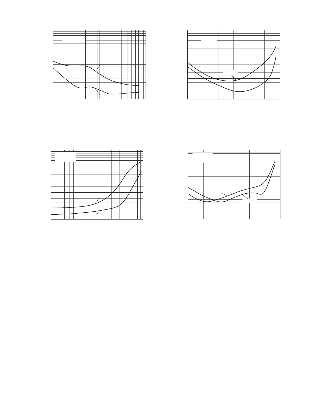
TYPICAL PERFORMANCE CURVES
-10
-20
-30
-40
-50
-60
OUTPUT LEVEL (dBV)
-70
-80
-90
-100 -90 - 80 -70 -60 -50 -40 -30 -20
4:1
Fig. 5 I/O Transfer function for Different Compression Ratios
2:1
3:1
1.2:1
1:1
INPUT LEVEL (dBV)
1.5:1
50
40
30
20
= -96dBV
V
IN
VIN = -80dBV
VIN = -60dBV
VIN = -40dBV
GAIN (dB)
10
0
-10
20 100 1k 10k 20k
VIN = -20dBV
FREQUENCY (Hz)
Fig. 6 Frequency Response for Different Input Levels
1.0
0.9
0.8
HI2
0.7
HI1
+R
R
HI1
0.6
R
( )
0.5
0.4
LO2
0.3
LO1
+R
R
LO1
0.2
R
0.1
0.0
1.0 1.4 1.8 2.2 2.6 3.0 3.4 3.8 4.0
COMPRESSION RATIO (RATIO)
Fig. 7 Compression Settings Resistor Ratio for High Pass
Channel (R
-10
COMPRESSION 1:1
-20
-30
-40
OUTPUT LEVEL (dBV)
-50
-50 -40 -30 -20
HI1
& R
) and Low Pass Channel (R
HI2
INPUT LEVEL (dBV)
R
= 0Ω
M PO
R
M PO
R
M PO
R
M PO
Fig. 9 I/O Transfer Function for
Different RMPO Resistors
LO1
= 10kΩ
= 22kΩ
= 50kΩ
& R
LO2
50
VIN = -60dBV
40
30
20
GAIN (dB)
10
0
-10
20 100 1k 10k 20k
RVC = 220kΩ
RVC = 100kΩ
R
= 47kΩ
VC
R
= 22kΩ
VC
R
= 10kΩ
VC
FREQUENCY (Hz)
Fig. 8 Frequency Response for Different RVC Values
)
-10
-20
-30
RTH = ∞
-40
-50
OUTPUT LEVEL (dBV)
-60
-70
-100 -90 -80 -70 -60 -50 -40 30 -20
R
TH
R
= 47kΩ
TH
RTH = 100kΩ
RTH = 0Ω
RTH = 10kΩ
= 22kΩ
INPUT LEVEL (dBV)
Fig. 10 I/O Transfer Function for
Different RTH Resistors
5
521 - 35 - 03
Page 6

1000
1000
198kΩ
100
10
RESISTOR VALUE (kΩ)
AG_C
R
1
-100 -90 -80 -70 -60 -50 -40 30 -20
9kΩ
INPUT LEVEL (dBV)
Fig. 11 Stage A Compressor Feedback Resistor Value
50
Rƒc = ∞
40
30
20
GAIN (dB)
10
0
-10
20 100 1k 10k 20k
1:1 in Low Frequency
4:1 in High Frequency
Crossover
Frequency
4:1 in Low Frequency
1:1 in High Frequency
FREQUENCY (Hz)
VIN = -80dBV
Fig. 13 Crossover Frequency Representation
for GR3031 Processor
1.6MΩ
100
72kΩ
10
RESISTORS VALUES (kΩ)
L
& R
H
R
15kΩ
1
-100 -90 -80 -70 -60 -50 -40 30 -20
2:1
1:1
4:1
INPUT LEVEL (dBV)
Fig. 12 Expander / Compressor Resistors Values
50
Rƒc = ∞
40
30
20
GAIN (dB)
10
0
-10
1:1 in Low Frequency
4:1 in High Frequency
20 100 1k 10k 20k
Crossover
Frequency
4:1 in Low Frequency
1:1 in High Frequency
FREQUENCY (Hz)
VIN = -80dBV
Fig. 14 Crossover Frequency Representation
for GR3032 Processor
50
1:1 in Low Frequency Gain
4:1 in High Frequency
40
30
20
GAIN (dB)
10
0
-10
20 100 1k 10k 20k
Rƒc=∞
100kΩ
47kΩ
22kΩ
10kΩ
0Ω
FREQUENCY (Hz)
Fig. 15 GR3031 Frequency Response
for Different Rƒc Resistor Values
521 - 35 - 03
VIN = -80dBV
50
1:1 in Low Frequency Gain
4:1 in High Frequency
40
30
20
GAIN (dB)
10
0
-10
20 100 1k 10k 20k
Rƒc=∞
100kΩ
47kΩ
22kΩ
10kΩ
0Ω
FREQUENCY (Hz)
Fig. 16 GR3032 Frequency Response
for Different Rƒc Resistor Values
6
VIN = -80dBV
Page 7
10
VIN = -40dBV
10
ƒ= 1 kHz
1
GR3032
THD & NOISE (%)
0.1
GR3031
100 1k 10k
FREQUENCY (Hz)
Fig. 17 THD and Noise vs Frequency
10
VIN = -40dBV
∆ƒ = 200Hz
1
IMD (%)
GR3031
1
THD & NOISE (%)
0.1
-80 -70 -60 -50 -40 -30 -20
GR3032
GR3031
INPUT LEVEL (dBV)
Fig. 18 THD and Noise vs Input Level
10
ƒ = 4kHz
∆ƒ = 200Hz
1
IMD (%)
0.1
GR3031
GR3032
0.1
3k 10k 100k
GR3032
FREQUENCY (Hz)
Fig. 19 Intermodulation Distortion (CCIF) vs Frequency
0.01
-80 -70 -60 -50 -40 -30 -20
INPUT LEVEL (dBV)
Fig. 20 Intermodulation Distortion
(CCIF) vs Input Level
7
521 - 35 - 03
Page 8

PAD POSITION PAD DIMENSION
Pad
No.
X Y X dim. Y dim.
1 0.0 0.0 20.0 20.0
2 31.0 0.0 20.0 20.0
3 62.0 0.0 20.0 20.0
4 92.0 0.0 20.0 20.0
5 122.0 0.0 20.0 20.0
6A 152.0 0.0 20.0 20.0
6B 182.0 0.0 20.0 20.0
7 212.0 0.0 20.0 20.0
8 217.0 43.0 20.0 20.0
9 212.0 85.0 20.0 20.0
10 182.0 85.0 20.0 20.0
11 152.0 85.0 20.0 20.0
12 122.0 85.0 20.0 20.0
13 92.0 85.0 20.0 20.0
14 62.0 85.0 20.0 20.0
15 31.0 85.0 20.0 20.0
16 0.0 85.0 20.0 20.0
17 -3.0 43.0 20.0 20.0
1 0.000 0.000 0.508 0.508
2 0.787 0.000 0.508 0.508
3 1.575 0.000 0.508 0.508
4 2.337 0.000 0.508 0.508
5 3.099 0.000 0.508 0.508
6A 3.861 0.000 0.508 0.508
6B 4.623 0.000 0.508 0.508
7 5.385 0.000 0.508 0.508
8 5.512 1.092 0.508 0.508
9 5.385 2.159 0.508 0.508
10 4.623 2.159 0.508 0.508
11 3.861 2.159 0.508 0.508
12 3.099 2.159 0.508 0.508
13 2.337 2.159 0.508 0.508
14 1.575 2.159 0.508 0.508
15 0.787 2.159 0.508 0.508
16 0.000 2.159 0.508 0.508
17 -0.076 1.092 0.508 0.508
Note: Centre of pad 1 has coordinates 0,0.
MIL
mm
0.250
(6.35)
XXXXXX
GR3032
0.090 MAX
(2.28)
16 15 14 13 12 11 10 9
0.115
(2.92)
Dimension units are in inches.
Dimensions in parenthesis are in millimetres converted
from inches and include minor rounding errors.
1.0000 inches = 25.400 mm.
Dimension ±0.003 ( ±0.08) unless otherwise stated.
XXXXXX - work order number.
Component name either GR3031 or GR3032.
This hybrid is designed to be reflowable for Gennum's reflow process profile.
Contact Gennum Representative for pad layout in electronic format.
0.015
(0.38)
17
1
0.0165
(0.42)
2 3 4 5 6a 6b 7
Fig. 21 Hybrid Layout & Dimensions
8
DOCUMENT IDENTIFICATION: DATA SHEET
The product is in production. Gennum reserves the right to make
changes at any time to improve reliability, function or design, in
order to provide the best product possible.
REVISION NOTES:
Updated to Data sheet
Gennum Corporation assumes no responsibility for the use of any circuits described herein and makes no representations that they are free from patent infringement.
521 - 35 - 03
© Copyright August 1995 Gennum Corporation. All rights reserved. Printed in Canada.
8
 Loading...