

Page 1
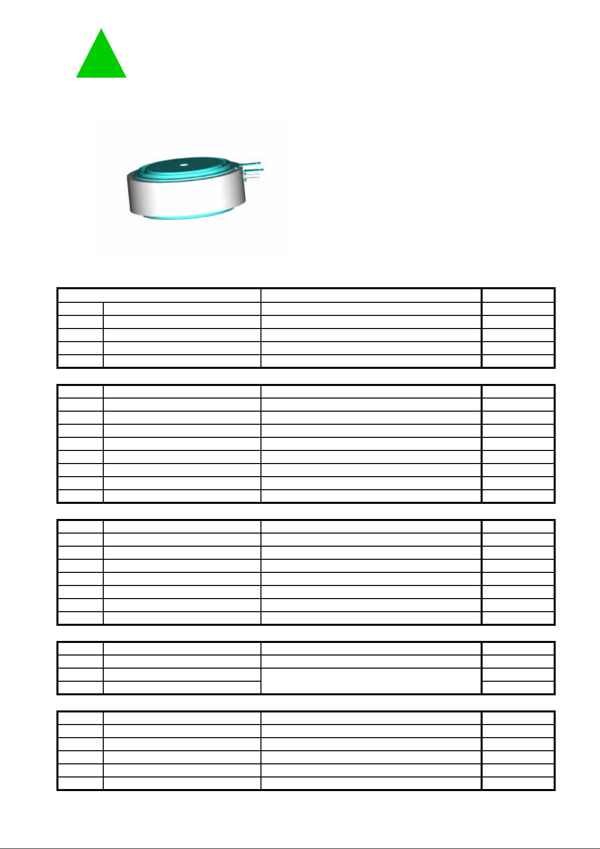
GPTJ2060
PHASE CONTROLLED SCR
I
V
, single phase, half wave, Tj = Tjmax
r
Ω
I
Tj = 25 °C
V
VR = 100 V, dV/dt = 20 V/µs
Green Power
Semiconductors
GPS - Green Power Semiconductors SPA
Factory: Via Ungaretti 10, 16157 Genova, Italy
High reliability operation
DC power supply
AC drives
Phone: +39-010-667 1307
Fax: +39-010-667 2459
Web: www.gpsemi.it
E-mail: info@gpsemi.it
VOLTAGE UP TO 1600 V
AVERAGE CURRENT 600 A
SURGE CURRENT 8 kA
BLOCKING CHARACTERISTICS
Characteristic Conditions
VRRM
VRSM
VDRM
IDRM
RRM
Repetitive peak reverse voltage 1600 V
Non-repetitive peak reverse voltage 1700 V
Repetitive peak off-state voltage 1600 V
Repetitive peak off-state current, max.
Repetitive peak reverse current, max.
VDRM, single phase, half wave, Tj = Tjmax
RRM
Value
30 mA
30 mA
ON-STATE CHARACTERISTICS
IT(AV)
IT(RMS)
ITSM
I²t I² t for fusing coordination 320 kA²s
VT(TO)
T
VTM
IH
L
Average on-state current Sine wave,180° conduction, Th = 55 °C 600 A
R.M.S. on-state current Sine wave,180° conduction, Th = 55 °C 942 A
Surge on-state current
Threshold voltage
On-state slope resistance
Peak on-state voltage, max
Holding current, max
Latching current, typ
Non rep. half sine wave, 50 Hz, VR = 0 V, Tj = Tjmax
Tj = Tjmax
Tj = Tjmax
On-state current IT =
Tj = 25 °C
1260 A , Tj = 25 °C 1,53 V
8 kA
0,96 V
0,46
150 mA
300 mA
m
TRIGGERING CHARACTERISTICS
VGT
IGT
VGD
PGM
PG(AV)
IFGM
VFGM
RGM
Gate trigger voltage Tj = 25 °C, VD = 12 V 3 V
Gate trigger current Tj = 25 °C, VD = 12 V 300 mA
Non-trigger voltage VD = 67% VRRM, Tj = Tjmax 0,25 V
Peak gate power dissipation Pulse width 0.5 ms 100 W
Average gate power dissipation 5 W
Peak gate current 20 A
Peak gate voltage (forward) 10 V
Peak gate voltage (reverse) 3 V
SWITCHING CHARACTERISTICS
di/dt Critical rate of rise of on-state current
dV/dt Critical rate of rise of off-state voltage
tq
Turn-off time, typ
Tj = Tjmax
Tj = Tjmax
Tj = Tjmax, IT = 400 A, di/dt = -12.5 A/µs
200 A/µs
1000 V/µs
200 µs
THERMAL AND MECHANICAL CHARACTERISTICS
Rth(j-c)
Rth(c-h)
Tjmax
Tstg
F Clamping force ± 10% 7 kN
Document GPTJ2060T001
Thermal resistance (junction to case) Double side cooled 0,056 °C/W
Thermal resistance (case to heatsink) Double side cooled 0,015 °C/W
Max operating junction temperature 125 °C
Storage temperature -40 / 125 °C
Mass 180 g
Page 2

Maximum surge current
Green Power
120°
60°
30°
Semiconductors
PHASE CONTROLLED SCR GPTJ2060
Current rating - sine wave
130
120
110
100
90
80
70
60
Heatsink temperature [°C]
50
60°
30°
0 200 400 600
IT [A]
d.s. cooled
9
8
7
6
5
[A]
4
TSM
I
3
2
1
0
1 10 100
Number of cycle current pulses [n]
Power loss - sine wave
1200
1000
[W]
F
P
800
600
400
90°
180°
200
180°90° 120°
0
0 100 200 300 400 500 600
IT[A]
On-state voltage drop
On-state voltage drop
1400
1400
1200
1200
1000
1000
800
800
[A]
[A]
T
T
I
600
I
600
400
400
200
200
0
0
0 0,5 1 1,5 2
0 0,5 1 1,5 2
Tj=T
VT [V]
VT [V]
jmax
Tj=T
jmax
Thermal impedance (j-c)
0,06
0,05
0,04
0,03
[°C / W]
0,02
TH(j-c)
Z
0,01
0
0,001 0,01 0,1 1 10 100
Time [s]
In the interest of product improvement Green Power Semiconductors reserves the right to change any specification given in this data
sheet without notice.
Document GPTJ2060T001
 Loading...