

Page 1
GP1S94
Subminiature Wide-gap Type
GP1S94
■■
Features
1. Subminiature wide-gap type
2. Emitter-detector gap width : 3.5 mm
3. Slit : (0.3) mm
4. With positioning boss
■
Applications
1. FDDs
2. Laser disc players
3. VCRs
Photointerrupter
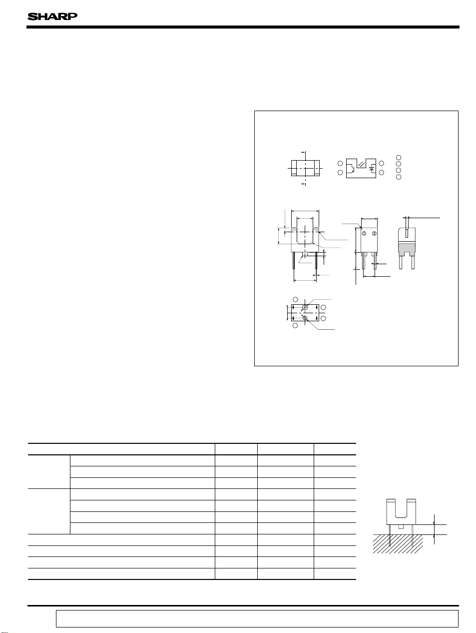
Outline Dimensions
Top View
aa
6.0
3.5
(0.85)
3.5
(
C0.2
❈ 5.0
3
1.1
1.2
2
Circuit diagram : Top View
3
(
Optical
center
(
)
C0.3
)
0.8
+ 0.2
0.15
- 0.1
+ 0
φ 1.1
- 0.1
4
1
+ 0
φ 0.9
- 0.1
C0.4
(Unit : mm)
1 Anode
12
2 Collector
3 Emitter
4
4 Cathode
a-a section
(
3.4
)
5.2
S
4 Z
0.4
❈ 2.54
3.6± 0.5
* Tolerance : ± 0.2
* Burrs dimensions : 0.15 MAX.
*( ) : Reference dimensions
The dimensions indicated by ❈ refer
to those measured from the lead base.
0.3)Slit width
■
Absolute Maximum Ratings
(Ta=25˚C)
Parameter Symbol Rating Unit
Forward current
Input
Reverse voltage
Power dissipation
Collector-emitter voltage
Output
Emitter-collector voltage
Collector current
Collector power dissipation
Total power dissipation
Operating temperature
Storage temperature
*1
Soldering temperature
*1 For MAX. 5 seconds
“ In the absence of confirmation by device specification sheets, SHARP takes no responsibility for any defects that occur in equipment using any of SHARP's devices, shown in catalogs,
data books, etc. Contact SHARP in order to obtain the latest version of the device specification sheets before using any SHARP's device.”
I
F
V
R
50 mA
6V
P75mW
V
CEO
V
ECO
I
C
P
C
P
tot
T
opr
T
stg
T
sol
35 V
6V
20 mA
75 mW
100 mW
-
25
to +
-
40 to + 100
85
˚C
˚C
260 ˚C
Soldering area
1 mm or more
Page 2

Electro-optical Characteristics
■
Parameter Symbol Conditions MIN. TYP. MAX. Unit
Input
Output
Forward voltage
Reverse current
Dark current
Collector current
Transfer
characteristics
Collector-emitter saturation voltage
Response time
Rise time
Fall time
GP1S94
(Ta=25˚C)
V
I
I
CEO
I
V
CE(sat
t
t
IF= 20mA - 1.2 1.4 V
F
VR=3V - - 10 µA
R
VCE= 20V - - 100 nA
VCE= 5V, IF= 5mA 40 - 400 µA
C
)
IF= 10mA, IC=40µA - - 0.4 V
= 5V, IC= 100 µ A
V
r
f
CE
= 1 000 Ω
R
L
- 50 150 µ s
- 50 150 µ s
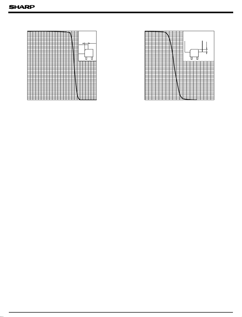
Fig. 1 Forward Current vs. Ambient
Temperature
60
50
)
mA
40
(
F
30
20
Forward current I
10
0
- 25 0 25 50 75 100
Ambient temperature Ta (˚C)
500
Ta= 75˚C
200
)
100
mA
(
50
F
20
10
5
Forward current I
2
1
0 0.5 1 1.5 2
50˚C
Forward voltage VF (V)
- 25˚C
85
25˚C
0˚C
2.5 3
Fig. 2 Power Dissipation vs. Ambient
Temperature
120
Total power dissipation
100
Input side power dissipation and
output side collector power dissipation
80
60
40
Power dissipation P (mW)
20
0
- 25 0 25 50 75 100
85
Ambient temperature Ta (˚C)
Fig. 4 Collector Current vs. Forward CurrentFig. 3 Forward Current vs. Forward Voltage
1.0
0.8
0.6
0.4
Collector current Ic (mA)
0.2
0
01020
Forward current IF (mA
VCE =5V
Ta =25˚C
)
Page 3

GP1S94
Fig. 5 Collector Current vs. Collector-emitter
Voltage
1.0
0.8
0.6
0.4
Collector current Ic (mA)
0.2
0
0428610
Collector-emitter voltage VCE (V
IF=50mA
40mA
30mA
20mA
10mA
5mA
)
Fig. 7 Collector-emitter Saturation Voltage
vs. Ambient Temperature
0.20
)
V
(
0.18
)
sat
(
CE
0.16
IF =10mA
C =40µ A
I
0.14
0.12
0.10
0.08
0.06
Collector-emitter saturation voltage V
- 25 0 25 50 75 85
Ambient temperature Ta (˚C)
Fig. 9 Response Time vs. Load Resistance
Fig. 6 Relative Collector Current vs.
Ambient Temperature
120
110
100
IF=5mA
V
CE=5V
90
80
70
60
50
40
30
Relative collector current (%)
20
10
0
- 25 0 25 50 75 85
Ambient temperature Ta (˚C)
Fig. 8 Dark Current vs. Ambient Temperature
-6
10
VCE= 20V
5
2
-7
10
)
A
(
5
CEO
2
-8
10
5
2
Dark current I
-9
10
5
2
-10
10
25 50 75 1000
Ambient temperature Ta (˚C)
1000
VCE =5V
C =100µA
I
500
100
50
10
Response time ( µs)
5
1
0.1 1 5 10 50 100
tf
tr
td
ts
Load resistance RL (kΩ
Test Circuit for Response Time
V
Input
R
D
CC
R
L
Output
)
Input
Output
10%
90%
t
t
d
s
t
r
t
f
Page 4
GP1S94
Fig. 10 Detecting Position Characteristics (1) Fig. 11 Detecting Position Characteristics (2)
100
90
80
70
60
50
40
30
20
Relative collector current (%)
10
0
0 0.5 1 1.5 2 2.5
IF =5mA
VCE =5V
L=0
Shield distance L (mm)
Please refer to the chapter "Precautions for Use".
●
100
L
90
80
70
60
50
40
30
20
Relative collector current (%)
10
0
0 0.5 1 1.5 2
IF =5mA
V
CE =5V
L
L=0
Shield distance L (mm)
 Loading...