

Page 1
GP1S59
GP1S59
Horizontal Slit Type
Photointerrper
■ Features
1. Horizontal slit type
2. PWB mouning type
3. Gap between light emitter and detector: 4.2mm
4. Slit width: 0.5mm
5. With a positioning boss
■ Applications
1. OA equipment, such as printers etc.
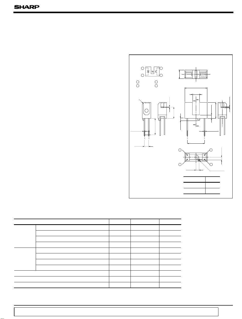
■ Outline Dimensions
Internal connection diagram
23
1 Anode
2 Cathode
C1
+
0.3
0.45
-
0.1
(
)
2.54
41
3 Collector
4 Emitter
AA'section
MIN 10
5.2
0.5
6.8
(
Unit : mm
JAPAN
S59
±
0.3
13.5
±
0.2
4.2
A
B
0.2
±
B'
1.3
4
Dimensions(d
* ( ): Reference dimensions
A'
0.4
(10)
1.8
* Unspecified tolerances shall be as follows ;
4.0< d<=18.0 ± 0.2
)
Tolerance
d<=4.0 ± 0.1
BB'section
9.3
2
+
0.3
-
0.1
1
23
φ 1.2
+
-
1.65
0.2
0.1
)
0.5
■ Absolute Maximum Ratings
(
Ta= 25˚C
)
Parameter Symbol Rating Unit
Input
Forward current I
*1
Peak forward current I
Reverse voltage V
F
FM
R
50 mA
1A
6V
Power dissipation P 75 mW
Output
Collector-emitter voltage V
Emitter-collector voltage V
Collector current I
Collector power dissipation P
Operating temperature T
Storage temperature T
*2
Soldering temperature T
CEO
ECO
C
C
opr
stg
sol
*1 Pulse width<=100µs, Duty ratio: 0.01
*2 For 5 seconds
“ In the absence of confirmation by device specification sheets, SHARP takes no responsibility for any defects that occur in equipment using any of SHARP's devices, shown in catalogs,
data books, etc. Contact SHARP in order to obtain the latest version of the device specification sheets before using any SHARP's device.”
35 V
6V
20 mA
75 mW
- 25 to + 85 ˚C
- 40 to + 100 ˚C
260 ˚C
Page 2
GP1S59
■ Electro-optical Characteristics
Parameter Symbol Condition MIN. TYP. MAX. Unit
Forward voltage V
Input
Output I
Transfer
chara
cteristics
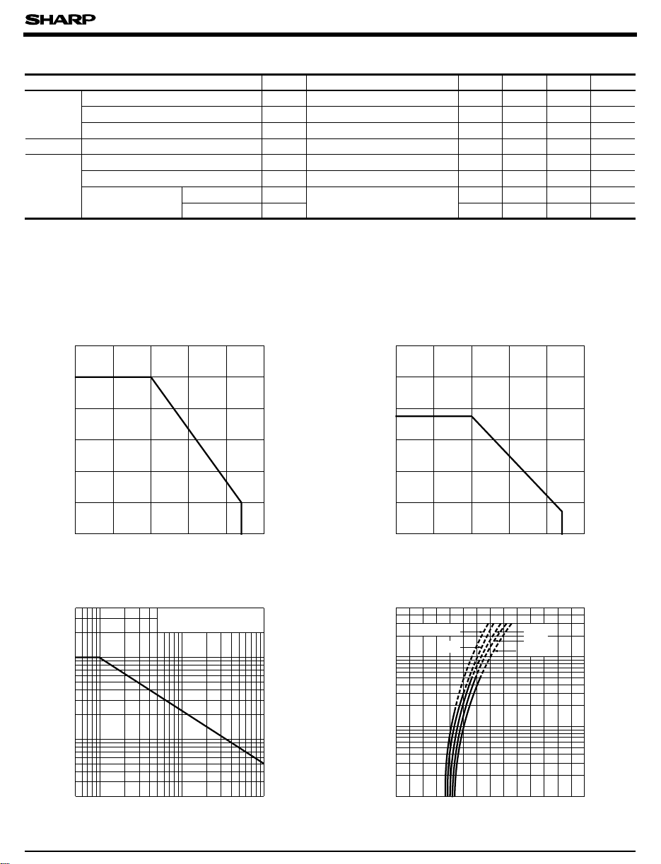
Fig. 1 Forward Current vs. Ambient
Temperature
)
mA
(
F
Forward current I
Fig. 3 Peak Forward Current vs.
Duty Ratio
)
mA
(
FM
Peak forward current I
Peak forward voltage V
Reverse current I
Collector dark current
Collector current I
Collector-emitter saturation voltage
Response time
60
50
40
30
20
10
0
- 25 0 25 50 75 100
Ambient temperature Ta (˚C
2000
1000
500
200
100
50
20
-2
55252
10
Duty ratio
Rise time t
Fall time t
)
Pulse width <= 100µ s
T
= 25˚C
a
-1
10
85 - 25 0 25 50 75 100
V
FM
R
CEO
C
CE(sat
r
f
(
Ta= 25˚C
F
IF= 20mA - 1.25 1.4 V
I-34V
= 0.5A
FM
VR=3V - - 10 µA
VCE= 20V - 1 100 nA
VCE= 5V, IF= 20mA 0.5 - 10.0 mA
)
IF= 40mA, IC= 0.5mA - - 0.4 V
VCE= 2V, IC= 2mA
= 100 Ω
R
L
-315
-420
)
µ s
µ s
Fig. 2 Collector Power Dissipation vs.
Ambient Temperature
120
)
100
mW
(
C
80
75
60
40
20
Collector power dissipation P
0
Ambient temperature Ta (˚C
85
)
Fig. 4 Forward Current vs.
Forward Voltage
500
Ta= 75˚C
200
)
100
mA
(
50
F
20
10
5
Forward current I
2
0
10
1
0 0.5 1 1.5 2
50˚C
Forward voltage VF (V
25˚C
0˚C
-
25˚C
2.5 3
)
3.5
Page 3

GP1S59
Fig. 5 Collector Current vs.
Forward Current
5
VCE=5V
T
= 25˚C
a
4
)
mA
(
C
3
2
Collector current I
1
0
Forward current IF (mA
Fig. 7 Collector Current vs.
Ambient Temperature
3.0
IF= 20mA
V
=5V
CE
2.5
)
mA
2.0
(
C
1.5
1.0
Collector current I
0.5
0
-25 0 25 50 75 100
Ambient temperature Ta (˚C
Fig. 9 Response Time vs.
Load Resistance
100
VCE=2V
= 2mA
I
C
50
= 25˚C
T
a
20
)
10
µ s
(
5
2
1
Response time
0.5
0.2
0.1
0.01 0.02 0.05 0.1 0.2 0.5 1 2 5 10
t
f
t
r
t
d
t
s
Load resistance R
L
(kΩ
Fig.6 Collector Current vs.
Collector-emitter Voltage
5
T
= 25˚C
a
4
)
mA
(
C
3
2
Collector current I
1
50403020100
)
Collector-emitter voltage VCE (V
= 50mA
I
F
40mA
30mA
20mA
10mA
1098765432100
)
Fig. 8 Collector-emitter Saturation Voltage
Ambient Temperature
0.25
)
V
(
)
0.2
sat
(
CE
0.15
0.1
0.05
Collector-emitter saturation voltage V
0
-25 0 25 50 75 100
)
Ambient temperature T
IF= 40mA
I
= 0.5mA
C
)
(˚C
a
Test Circuit for Response Time
V
Input
R
D
CC
R
L
Output
)
Input
Output
10%
90%
t
t
d
s
t
r
t
f
Page 4

GP1S59
Fig.10 Frequency Response
0
)
dB
-5
(
R
= 10kΩ
5
3
10
L
4
10
Frequency f (Hz
-10
Voltage gain Av
-15
-20
2 252525
10
)
VCE=2V
= 2mA
I
C
T
= 25˚C
a
1kΩ 100Ω
5
6
10
Fig.11 Collector Dark Current vs.
Ambient Temperature
-6
10
)
A
(
10
CEO
10
10
Collector dark current I
10
= 20V
V
CE
5
2
-7
5
2
-8
5
2
-9
5
2
-10
- 25 25 50 75 100
0
Ambient temperature Ta (˚C
)
Fig.12 Relative Collector Current vs. Fig.13 Relative Collector Current vs.
Shield Distance (1
100
90
)
80
%
(
70
60
50
40
30
Relative collector current
20
10
0 0
Shield distance L (mm
)
IF= 20mA VCE=5V
Ta= 25˚C
Shied
Detector
0
(
Detector center
0- 0.5- 1.0- 1.5- 2.0 0.5 1.0 1.5 2.0
)
L
+
)
Shield Distance (2
100
90
)
80
%
(
70
60
50
40
30
Relative collector current
20
10
Shield distance L (mm
)
IF= 20mA VCE=5V
Ta= 25˚C
Shield
L
Detector
0- 0.5- 1.0- 1.5- 2.0 0.5 1.0 1.5 2.0
)
0
+
)
Detector center
(
■ Precautions for Use
(1)
In case of cleaning, use only the following type of cleaning solvent.
Ethyl alcohol, Methyl alcohol, Isopropyl alcohol
(2)
As for other general cautions, refer to the chapter “Precautions for Use”.
 Loading...