

Page 1
GP1S38/GP1S381
GP1S38/GP1S381
Optical Guide Photointerrupter
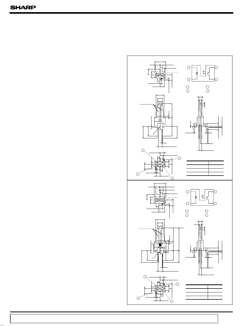
■ Features ■ Outline Dimensions
1. Optical guide for setting detecting position
that can be devided into Assy substrate
(mather substrate
)
without leads, connectors, etc.
2. PWB mounting type
3. Easy mounting to PWB due to the holder
with hook
4. Gap between light emitter and detector:
GP1S38:2mm
GP1S381:3mm
■ Applications
1. VCRs
GP1S38
Optical guide
(
Transparency
)
14.6
(
1
0.1-0.1
+
5.5
4
GP1S381
Optical guide
(
Transparency
( 14.6 )
1
0.1
±
5.5
φ
4
6
( 1.5 )
)
12.6
(
φ
1
6
( 2.5 )
( 12.6 )
+ 0
1
- 0.05
4.5
2 - 1.5
3.5
3.2
+
-
6.5
2.8
2 - 1.5
4
3.2
6.5
4.25
)
1.8
RO.5
+
-
0.1
0.1
5.25
)
2 - 1.5
RO.5
+
0.1
-
0.1
0.1
0.1
8.9
8.3
5
(
7.16
11
+
0
-
0.1
5
2
+
4
-
12
+ 0
- 0.1
)
3
2-2
4.5±0.1
2 - 2.5
(
0.5
*( 3.85 )
φ
0.1
0.1
2 - 2.5
Max. 0.4
0.5
*( 4.85 )
φ 1.5
2 - 0.9
φ 1) Hole
5.75
( 1.5 )
1.2
8.9
)
12.6
(
+0.15
-
0.1
+
1.5
-
4.9
0.1-0.1
+
5
3
2 - 3
2 - 0.9
(
φ 1) Hole
5.75
( 1.5 )
11.6
1.2
8.9
2 - 1.5
( 12.6 )
+
0.15
-
0.1
+ 0
- 0.05
4.9
5 ±0.1
3
+0-
0.1
0.1
0.2
14.5
)
14.6
(
0.15
±
2
(
Unit : mm
Internal connection diagram
4
1
1 Anode
2 Collector
3
2
1.5
3 Emitter
4 Cathode
0.2
2 - 0.3
2 - 7
2 - 1
2 - 1
*(2.54 )
* Unspecified tolerances
2
shall be as follows;
Dimensions(d
5.0<=d<
15.0<=d
)
Tolerance
d<
± 0.2
5.0
± 0.25
15.0
± 0.3
* ( ): Reference dimensions
Internal connection diagram
4
1
20.5
( 14.6 )
1 Anode
2 Collector
2 - 0.3
0.2
2.1
3 Emitter
4 Cathode
3
1.8
2 - 7
2 - 1
2 - 1
*( 2.54 )
* Unspecified tolerances
shall be as follows;
Dimensions(d)Tolerance
d< 5.0 ± 0.2
5.0<=d< 15.0 ± 0.25
15.0<=d ± 0.3
* ( ): Reference dimensions
)
3
2
0.05-0
+
3.0
1.65
-
-
2
2
2 - 0.3
3 - 3.45
3
2
0.05-0
+
1.65
-
2 - 3.0
2
2 - 0.3
3 - 3.45
“ In the absence of confirmation by device specification sheets, SHARP takes no responsibility for any defects that occur in equipment using any of SHARP's devices, shown in catalogs,
data books, etc. Contact SHARP in order to obtain the latest version of the device specification sheets before using any SHARP's device.”
Page 2
GP1S38/GP1S381
■ Absolute Maximum Ratings
Parameter Symbol Rating Unit
Input
Forward current I
*1
Peak forward current I
Reverse voltage V
F
FM
R
Power dissipation P 150 mW
Collector-emitter voltage V
Output
Emitter-collector voltage V
Collector current I
Collector power dissipation P
Operating temperature
Storage temperature T
*2
Soldering temperature T
*1 Pulse width <= 100µ s, Duty ratio: 0.01
*2 3 seconds or less at the position of 1mm or more from the surface of resin
CEO
ECO
C
C
T
opr
stg
sol
■ Electro-optical Characteristics
Parameter Symbol Conditions MIN. TYP. MAX. Unit
V
F
V
FM
I
R
I
CEO
I
C
)
V
CE(sat
r
f
Input
Output
Transfer
characteristics
Forward voltage
Peak forward voltage
Reverse current
Collector dark current
Collector current
Collector-emitter saturation voltage
Response time
Rise time t
Fall time t
(
Ta = 25˚C
)
60 mA
1A
6V
35 V
6V
20 mA
50 mW
- 25 to + 80 ˚C
- 40 to + 80 ˚C
260 ˚C
(
Ta= 25˚C
IF= 50mA - - 1.5 V
IFM= 0.5A - - 3.5 V
VR=3V - - 10 µA
VCE= 20V - - 100 nA
VCE= 5V, IF= 20mA 100 - - µ A
IF= 40mA, IC=30µA - - 0.4 V
VCE= 10V, IC=50µA
= 100k Ω
R
L
- 0.85 2.5 ms
- 0.75 2.1 ms
)
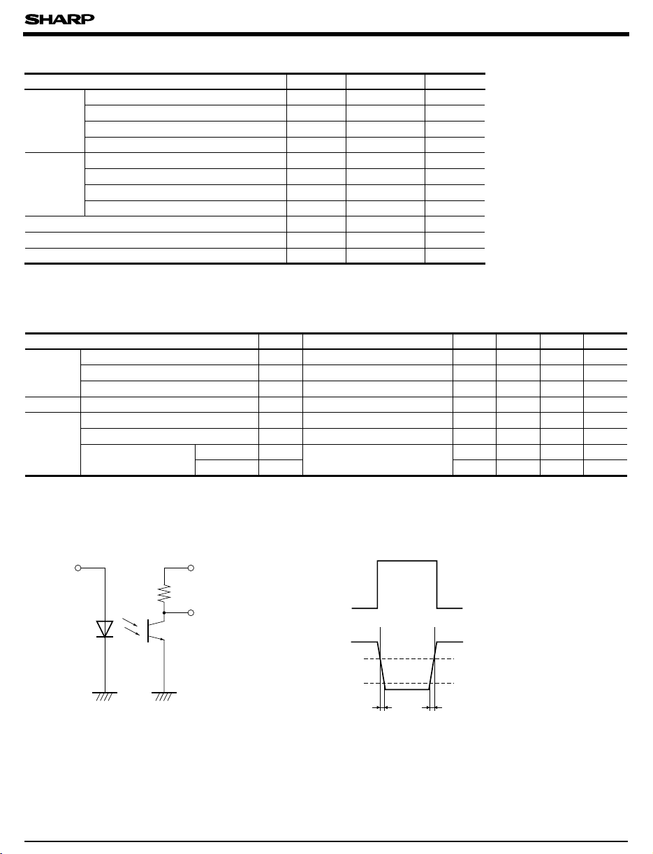
■ Test Circuit for Response Time
Vcc
R
L
Measuring terminal
Input
Output
10%
90%
tr tf
Page 3

GP1S38/GP1S381
Fig. 1 Forward Current vs.
Ambient Temperature
70
60
)
50
mA
(
F
40
30
Forward current I
20
16
10
0
-25
0255075
Ambient temperature T
a
Fig. 3 Peak Forward Current vs.
Duty Ratio
2000
)
1000
mA
(
500
FM
200
100
50
Peak forward current I
20
-3
10
25
-2
25 25
10
10
Duty ratio
Forward Current
5.0
)
4.0
mA
(
C
3.0
2.0
Collector current I
1.0
)
(˚C
Pulse
width<=100ms
T
= 25˚C
a
- 1
VCE=5V
T
= 25˚C
a
Fig. 2 Collector Power Dissipation vs.
Ambient Temperature
)
100
mW
(
C
80
60
50
40
22.5
20
Collector power dissipation P
0
10080
-25
0255075
)
Ambient temperature T
a
(˚C
10080
Fig. 4 Forward Current vs.
Forward Voltage
)
mA
(
F
500
200
100
50
T
= 75˚C
a
50˚C
25˚C
0˚C
- 20˚C
20
10
5
Forward current I
2
1
0
10
0
Forward voltage V
)
(V
F
3.53.02.52.01.51.00.5
Fig. 6 Collector Current vs.Fig. 5 Collector Current vs.
Collector-emitter Voltage
= 25˚C
T
5.0
)
4.0
mA
(
C
3.0
2.0
Collector current I
1.0
I
F
a
= 60mA
50mA
40mA
30mA
20mA
10mA
12 36
Forward current I
(mA
F
0
60544842302418006
)
0
Collector-emitter voltage V
864
102
)
(V
CE
Page 4

GP1S38/GP1S381
Fig. 7 Collector Current vs.
Ambient Temperature
1.4
1.2
)
1.0
mA
(
C
0.8
0.6
0.4
Collector current I
0.2
0
-25
0255075
Ambient temperature Ta (˚C
I
= 20mA
F
V
CE
=5V
)
Fig. 9 Response Time vs.
Load Resistance
1000
VCE= 10V
I
= 50mA
C
T
= 25˚C
a
)
100
ms
(
10
Response time
1
Fig.11 Relative Collector Current vs.
Shield Distance (1
100
90
)
%
(
80
70
60
50
40
30
Relative collector current
20
10
1234567
t
f
t
r
t
d
t
s
0.1 1 10
Load resistance R
L
(kΩ
)
(
Shield
Shield distance (1) L (mm
)
GP1S38
L
)
100
1000.01
Fig. 8 Collector-emitter Saturation Voltage vs.
Ambient Temperature
)
V
(
)
0.12
sat
(
CE
0.10
0.08
0.06
0.04
0.02
Collector-emitter saturation voltage V
0
-25
0255075
Ambient temperature Ta (˚C
IF= 40mA
I
= 30mA
C
)
100
Fig.10 Collector Dark Current vs.
Ambient Temperature
-6
10
V
= 20V
5
CE
)
2
A
(
-7
10
CEO
5
2
-8
10
5
2
-9
10
Collector dark current I
5
2
-10
10
-25
Fig.12 Relative Collector Current vs.
Shield Distance (2
)
100
90
)
%
(
80
70
60
50
40
30
Relative collector current
20
10
0 255075100
Ambient temperature T
a
(˚C
)
)
(
GP1S38
Shield
0123
Shield distance (2) L (mm
)
L
)
Page 5

GP1S38/GP1S381
Fig.13 Relative Collector Current vs.
Shield Distance (1
100
90
)
%
(
80
70
60
50
40
30
Relative collector current
20
10
1234567
Shield distance (1) L (mm
● Please refer to the chapter “ Precautions for Use”.
)
(
GP1S381
L
Shield
)
)(
Fig.14 Relative Collector Current vs.
Shield Distance (2
)
GP1S381
100
90
)
%
(
80
70
60
50
40
30
Relative collector current
20
10
0123
Shield distance (2) L (mm
Shield
)
)
L
 Loading...