

Page 1
Compact OPIC Photointerrupter
GP1A74A/GP1A74A1
with Connector
GP1A74A/GP1A74A1
■■
1. Compact type
2. TTL compatible owing to OPIC output
3. Snap-in mounting type
4. 3 kinds of mounting plate thickness
(Applicable plate thickness : 1.0, 1.2 and 1.6 mm)
■
Applications
1. Copiers
2. Laser beam printers
3. Facsimiles
* "OPIC" (Optical IC) is a trademark of the SHARP Corporation.
An OPIC consists of a light-detecting element and signal-processing circuit
integrated onto a single chip.
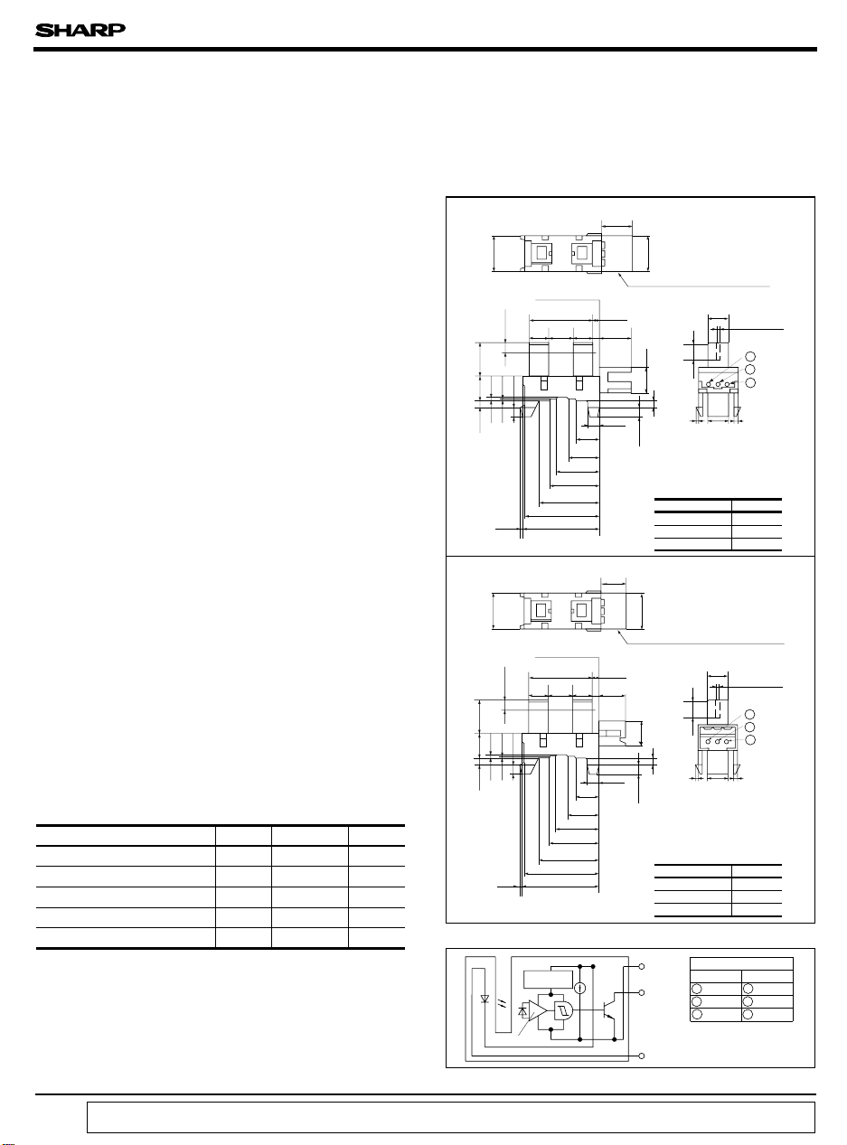
Outline DimensionsFeatures
GP1A74A
8.0
7.25.61.1
0.6
0.7
GP1A74A1
8.0
7.25.61.1
JAPAN
(Case surface)
4.3 4.3
(2.3)
(Sensor center)
2.3
0.2
JAPAN
(Case surface)
4.3 4.3
(Sensor center)
( 2.3)
13.6
5.0
16.8
17.0
13.6
5.0
11.4
13.8
(Unit : mm)
(6.8)
74
5.4
6.9
9.9
74
SHARP
1.6
6.8± 1
2.4
( 5)
SHARP
1.6
5.0±1
(7.8)
JAPAN AMP made
connector 175487-3
4.7
2-0.5 ± 0.1
3.2
(5.8)
1.1
2-0.5
2.3
* Unspecified tolerances
* ( ) : Connector dimensions
15.0 <= d
(8.0)
( 5)
3.4
shall be as follows.
for reference
Dimension
5.0<= d < 15.0
HIROSE made
connector DF3A-3P-2DSA
d < 5.0
3.2
4.7
Tolerance
2-0.5 ± 0.1
(Slit)
: V
1
: Vout
2
: GND
3
2-0.9
0.15
± 0.15
0.2
± 0.2
0.3
± 0.3
(Slit)
: V
3
: Vout
2
: GND
1
CC
CC
2.4
1.1
2-0.5
3.4
shall be as follows.
for reference
Dimension
d < 5.0
5.0<= d < 15.0
15.0 <= d
Connector terminal No.
GP1A74A
3 : GND
2 : Vout
1 : Vcc
13.8
16.8
17.0
Constant
voltage circuit
11.4
5.4
6.9
9.9
2.3
* Unspecified tolerances
* ( ) : Connector dimensions
GND
Vout
Vcc
2.3
0.6
■
Absolute Maximum Ratings
(Ta=25˚C)
0.2
Parameter Symbol Rating Unit
- 0.5 to + 7
Supply voltage
*1
Output voltage
*2
Low level output current
*3
Operating temperature
*3
Storage temperature
*1 Output transistor collector-emitter voltage
*2 Output transistor collector current
*3 The connector should be plugged in/out at normal temperature.
“ In the absence of confirmation by device specification sheets, SHARP takes no responsibility for any defects that occur in equipment using any of SHARP's devices, shown in catalogs,
data books, etc. Contact SHARP in order to obtain the latest version of the device specification sheets before using any SHARP's device.”
V
CC
V
- 0.5 to + 7
out
I
OL
T
opr
T
stg
8
-20to +75
-30to +85
V
V
mA
˚C
˚C
0.7
■
Internal Connection Diagram (Both GP1A74A/GP1A74A1)
Amp.
* GP1A74A andGP1A74A1 are different in the terminal marking number of
connectors from each other due to use of connectors of different manufacturers.
2-0.9
Tolerance
0.15
± 0.15
0.2
± 0.2
0.3
± 0.3
GP1A74A1
1 : GND
2 : Vout
3 : Vcc
Page 2
Electro-optical Characteristics
■
Parameter Symbol Conditions MIN. TYP. MAX. Unit
Operating supply voltage
Current consumption
Low level output voltage
Current consumption
High level output voltage
V
CC
I
Light beam uninterrupted
CCL
V
Light beam uninterrupted, I =4mA
OL
I
Light beam interrupted
CCH
V
Light beam interrupted, R =47kΩ
OH
-
GP1A74A/GP1A74A1
(Vcc=5v, Ta=25 ˚C unless otherwise specified)
4.5 - 5.5 V
- - 16.5 mA
OL
L
- - 0.35 V
- - 16.5 mA
VCCx 0.9
--V
Response
MIN. interruption time
characteristics
MIN. sensing time
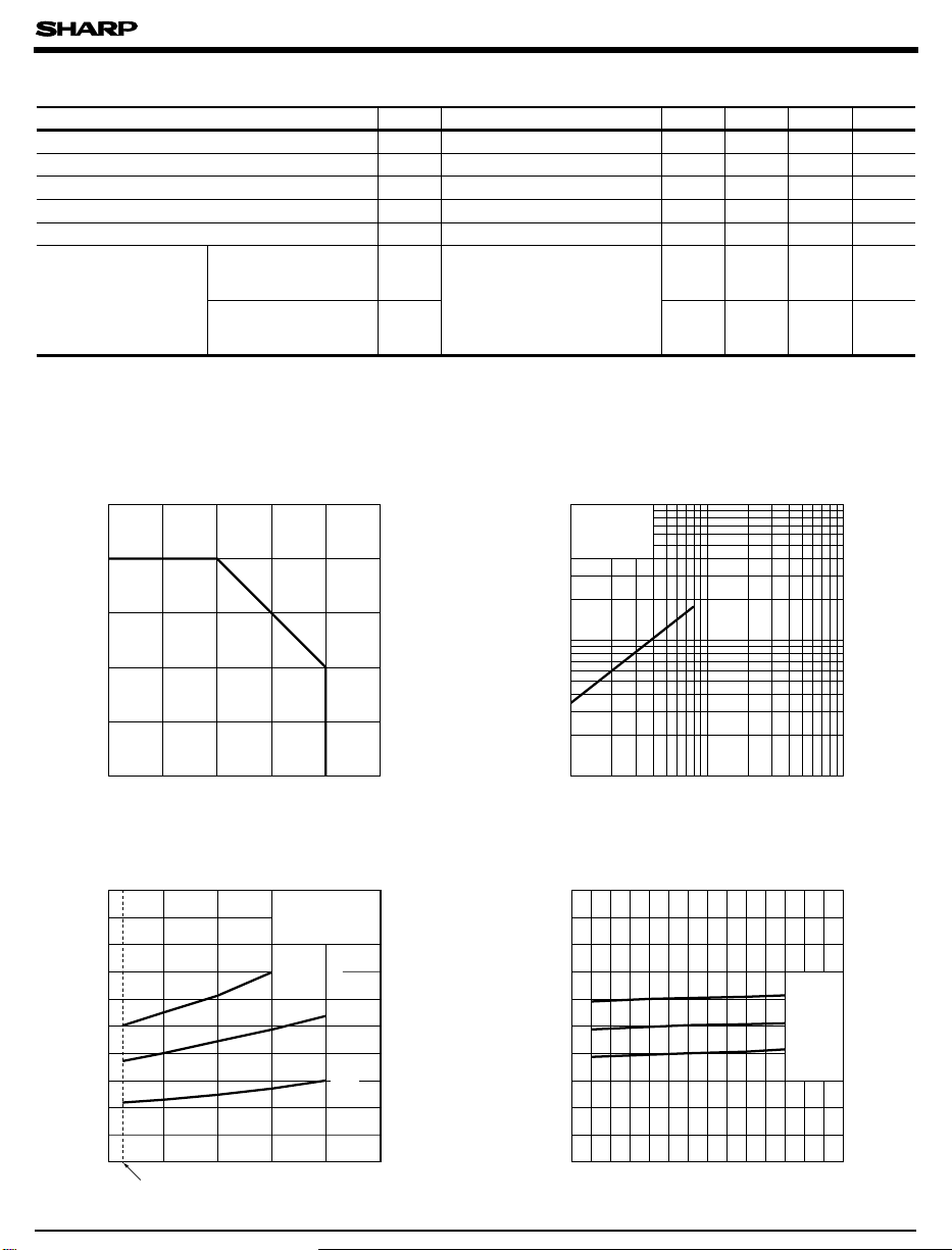
Fig. 1 Output Current vs. Ambient
Temperature
10
8
)
mA
(
6
OL
4
Output current I
2
0
- 20 0 25 50 75
Ambient temperature Ta (˚C)
Fig. 3 Low Level Output Voltage vs.
Ambient Temperature
0.2
V
=5V
I
OL
CC
= 6mA
)
V
(
OL
0.1
Low level output voltage V
0
- 25 0 25 50 75 100
-20
Ambient temperature Ta (˚C) Supply voltage VCC (V
4mA
2mA
t
H
R
= 4.7kΩ
L
t
L
166 - - µs
166 - - µs
Fig. 2 Low Level Output Voltage vs.
Low Level Output Current
1.0
=5V
V
CC
T
= 25˚C
)
V
(
OL
Low level output voltage V
a
0.5
0.2
0.1
0.05
0.02
0.01
1 5 10 50 100
202
Low level output current IOL (mA
)
Fig. 4 Supply Current vs. Supply Voltage
20
)
mA
(
CC
10
Supply current I
0
4.5 5.5
5.0
- 20˚CI
CCL
- 20˚CI
CCH
+25˚CI
CCL
+25˚CI
CCH
+75˚CI
CCL
+75˚CI
CCH
)
Page 3

GP1A74A/GP1A74A1
Fig. 5 Detecting Position Characteristics (1)
VCC= 5V, Ta= 25˚C
R
= 47kΩ
L
Detecting position
characteristics
(
d= 2.35± 0.3mm
012345 543210
)
0
d
Shield plate
Distance d (mm) Distance h (mm)
■
Recommended Mounting Hole Shape
General mounting type
Output "High"
Output "Low"
17
Fig. 6 Detecting Position Characteristics (2)
Output "High"
VCC=5V
T
= 25˚C
a
= 47kΩ
R
L
Detecting position
characteristics
+ 0.3
(
h= 3.0
Shield plate
- 1.8
mm
)
0
h
Output "Low"
(Unit : mm)
8 - R0.1± 0.1
66
17
8 - R0.1± 0.18 - R0.1± 0.1
3.53.5
17
7.5 7.5
7.7
Plate thickness : 1.6 mm
7.5
7.5
Plate thickness : 1.0 mmPlate thickness : 1.2 mm
12 - R0.1± 0.112 - R0.1± 0.1 12 - R0.1± 0.1
66
3.53.5
Reverse insertion
preventive type
7.7
17
7.5 7.5
2.42.4 2.4 2.4 2.4 2.4
7.5
Plate thickness : 1.6 mm
1.
It is recommended to mark the shear droop surface (punch side) of the mounting plate (metal plate) with "GP1A74A" or "GP1A74A1".
2.
Mounting workability, shaking after mounting and mounting strength depend on the corner radius of the mounting plate and state of punching.
17
7.5
Plate thickness : 1.0 mmPlate thickness : 1.2 mm
17
Determine the mounting dimensions after check on an actual machine.
3. General dimensional tolerances shall be ± 0.1 mm.
Page 4

GP1A74A/GP1A74A1
(Precautions for Operation)
1) In this product, the PWB is fixed with a hook, and cleaning solvent may remain inside the case;
therefore, dip cleaning or ultrasonic cleaning are prohibited.
2) Remove dust or stains, using an air blower or a soft cloth moistened in cleaning solvent.
However, do not perform the above cleaning using a soft cloth with solvent in the marking portion.
In this case, use only the following type of cleaning solvent for wiping off;
Ethyl alcohol, Methyl alcohol, Isopropyl alcohol,
When the cleaning solvents except for specified materials are used, please contact us.
3) In order to stabilize power supply line, connect a by-pass capacitor of more than 0.01µF between V and GND
near the device.
●
As for other general precautions, please refer to the chapter "Precautions for Use".
CC
 Loading...