

Page 1
OPIC Photointerrupter with
GP1A70R/GP1A71R
Encoder Functions
GP1A70R/GP1A71R
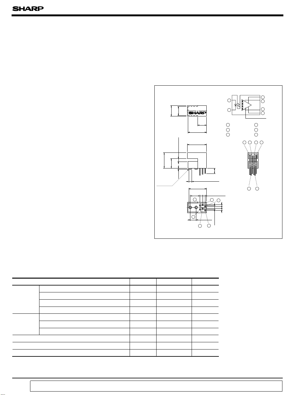
■ Features ■ Outline Dimensions
1. 2-phase (A, B) digital output
2. Sensing accuracy
(GP1A70R Disk slit pitch : 1.14mm
(GP1A71R Disk slit pitch : 0.7mm
3. PWB mounting type
(Lead bending type
)
4. TTL compatible output
5. Compact, lightweight
■ Applications
1. Printers
2. Copiers
3. Numerical control machines
)
)
0.15
±
10.5
2 - C0.2
*“OPIC” (Optical IC) is a trademark of the SHARP Corporation.
An OPIC consists of a light-detecting element and signal processing circuit integrated onto a single chip.
7.2
6.5
6.0
0.2-0.1
+
2.0
0.75
GP1A70R
6.0
12.5
13.0
2- φ 2.0
12.0
(
)
6.56
2
1
4.0
5
± 0.1
2 -(1.75
±
0.1
6
3
(
Unit : mm
Internal connection diagram
1
2
1 Anode
2 Cathode
3 V
OB
3456
MIN.
2.5
)
4
)
1.27
(
)
3 -
*Tolerance :± 0.3mm
2.54
(
*( ): Reference dimensions
6
5
4
3
4 GND
5 V
CC
6 V
OA
12
)
OPIC
■ Absolute Maximum Ratings
Parameter
Forward current I
*1
Input
Peak forward current I
Reverse voltage
(
Ta = 25˚C
Symbol Rating Unit
F
FM
V
R
50 mA
1A
6V
)
Power dissipation P 75 mW
Supply voltage V
Output
Low level output current I
Power dissipation P
Operating temperature T
Storage temperature T
*2
Soldering temperature T
*1 Pulse width<=100µs, Duty ratio 0.01
*2 For 5 seconds
“ In the absence of confirmation by device specification sheets, SHARP takes no responsibility for any defects that occur in equipment using any of SHARP's devices, shown in catalogs,
data books, etc. Contact SHARP in order to obtain the latest version of the device specification sheets before using any SHARP's device.”
CC
OL
O
opr
stg
sol
7V
20 mA
250 mW
0 to + 70 ˚C
- 40 to + 80 ˚C
260 ˚C
Page 2
GP1A70R/GP1A71R
■ Electro-optical Characteristics
Parameter Symbol
Input
Forward voltage V
Reverse current I
Operating supply voltage V
Output
High level output voltage V
Low level output voltage V
Supply current I
Transfer
characteristics
Duty ratio
Response frequency f
*3 Measured under the condition shown in Measurement Conditions.
*4 In the condition that output A and B are low level.
t
AH
: x 100, DB: x 100, Duty ratio: Average disk rotation time per turn
*5 D
A
t
AP
t
BH
t
BP
GP1A70R
GP1A71R
*5
DA, D
F
R
CC
OH
OL
CC
B
MAX.
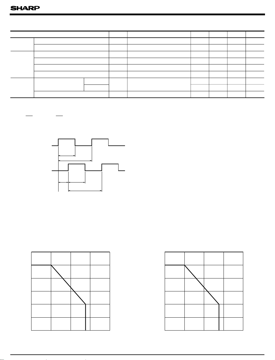
■ Output Waveforms
Output A
)
(V
OA
Output B
(V
OB
)
t
AH
t
AP
t
AB1
t
BH
t
BP
Rotational direction: Counterclockwise when seen
(
Ta= 25˚C unless otherwise specified
Conditions MIN. TYP. MAX. Unit
= 20mA, Ta= 25˚C - 1.2 1.4 V
I
F
VR= 3V, Ta= 25˚C
--10µA
4.5 5.0 5.5 V
*3
VCC= 5V, IF= 20mA 2.4 4.9 - V
*3
IOL= 8mA, VCC= 5V, IF= 20mA
*4
VCC= 5V, IF= 20mA - 5 20 mA
*3
VCC= 5V, IF= 20mA, f = 2.5kHz
*3
VCC= 5V, IF= 20mA - - 10 kHz
from OPIC light detector
- 0.1 0.4 V
25 50 75 %
25
50 %
75
)
Fig. 1 Forward Current vs. Ambient
Temperature
60
50
)
40
mA
(
F
30
20
Forward current I
10
0
0
Ambient temperature Ta (˚C
70
)
Fig. 2 Output Power Dissipation vs.
Ambient Temperature
300
)
250
mW
(
O
200
150
100
50
Output power dissipation P
0
100755025
0
Ambient temperature Ta (˚C
70
100755025
)
Page 3

GP1A70R/GP1A71R
Fig. 3-a Duty Ratio vs. Frequency
(
t
AH
x 100 (Output A
t
AP
t
BH
x 100 (Output B
t
BP
)
GP1A70R
80
70
60
)
%
(
50
Duty ratio
40
30
20
110
25
Frequency f (kHz
VCC=5V
I
= 20mA
F
T
= 25˚C
a
)
)
)
Fig. 4-a Phase Difference vs. Frequency
)
deg.
(
ABI
Phase difference θ
130
120
110
100
(
GP1A70R
t
AB1
θ= 360˚
AB1
t
AP
90
80
=5V
V
CC
IF= 20mA
T
= 25˚C
a
)
Fig. 3-b Duty Ratio vs. Frequency
Fig. 4-b Phase Difference vs. Freauency
(
t
AH
x 100 (Output A
t
AP
t
BH
x 100 (Output B
t
BP
(
θ
=
AB1
GP1A71R
V
=5V
CC
I
= 20mA
F
= 25˚C
T
a
)
GP1A71R
V
=5V
CC
I
= 20mA
F
t
AB1
x
360˚
t
AP
)
80
70
60
)
%
(
50
Duty ratio
40
30
20
12 510
130
120
)
deg.
(
110
AB1
100
90
Phase difference θ
80
Frequency f (kHz
)
)
)
70
Frequency f (kHz
Fig. 5-a Duty Ratio vs.
Ambient Temperature
80
70
60
)
%
(
50
Duty ratio
40
30
20
0
20 30
10
Ambient temperature T
52
)
(
GP1A70R
=5V
V
CC
I
= 20mA
F
f= 2.5kHz
t
AH
x
100 (Output A
t
AP
t
BH
x
100 (Output B
t
BP
40 50 60 70
a
(˚C
)
70
101
12 510
Frequency f (kHz
)
Fig. 5-b Duty Ratio vs.
)
)
)
Ambient Temperature
80
70
60
)
%
(
50
Duty ratio
40
30
20
020 70
Ambient temperature T
t
AH
t
AP
t
BH
t
BP
(
GP1A71R
VCC=5V
I
F
f= 2.5kHz
x
100 (Output A
x
100 (Output B
(˚C
a
)
= 20mA
)
)
6050403010
)
Page 4

GP1A70R/GP1A71R
Fig. 6-a Phase Difference vs. Ambient
Temperature
130
120
)
deg.
(
110
ABI
100
90
Phase difference θ
80
70
0
10
3020
Ambient temperature T
Fig. 7-a Duty Ratio vs.
Distance (Xdirection
80
70
60
)
%
(
50
Duty ratio
40
30
VCC=5V
I
= 20mA
F
f= 2.5kHz
t
AB1
a
(˚C
x
t
AP
)
θ= 360˚
AB1
)
(
GP1A70R
=5V
V
CC
I
= 20mA
F
f= 2.5kHz
T
= 25˚C
a
t
AH
100 (Output A
x
t
AP
t
BH
x
100 (Output B
t
BP
Fig. 6-b Phase Difference vs. Ambient
Temperature
130
120
)
deg.
(
110
AB1
100
90
Phase difference θ
80
70
70605040
020 70
Ambient temperature T
θ= 360˚
AB1
Fig. 7-b Duty Ratio vs.
)
)
)
Distance (X direction
80
70
60
)
%
(
50
Duty ratio
40
30
t
AH
x 100 (Output A
t
AP
t
BH
x 100 (Output B
t
BP
=5V
V
CC
I
= 20mA
F
f = 2.5kHz
t
AB1
x
t
AP
6050403010
)
(˚C
a
)
(
GP1A71R
=5V
V
CC
I
= 20mA
F
f= 2.5kHz
T
= 25˚C
a
)
)
)
20
- 1.0
Distance X (mm) (Shifting encoder
Fig. 8-a Phase Difference vs. Distance
(X direction
130
120
)
deg.
(
110
ABI
100
90
Phase difference θ
80
70
- 1.0
Distance X (mm) (Shifting encoder
)
θ= 360˚
AB1
Reference position
0 1.0
)
(
GP1A70R
=5V
V
CC
I
= 20mA
F
f= 2.5kHz
T
= 25˚C
a
t
AB1
x
t
AP
(+)(-)
GP1A70R
Disk
)
20
1.00
- 1.0 1.0
Distance X (mm) (Shifting encoder
Fig. 8-b Phase Difference vs. Distance
)
(X direction
140
130
)
deg.
(
120
AB1
110
100
Phase difference θ
90
80
- 1.0 1.0
Distance X (mm) (Shifting encoder
0
)
(
GP1A71R
θ= 360˚
AB1
Reference position
(+)(-)
0
=5V
V
CC
I
= 20mA
F
f= 2.5kHz
T
= 25˚C
a
t
AB1
x
t
AP
GP1A71R
Disk
)
)
)
Page 5

GP1A70R/GP1A71R
Fig. 9-a Duty Ratio vs.
Distance (Ydirection
80
70
60
)
%
(
50
Duty ratio
40
30
20
- 1.0
Distance Y (mm) (Shifting encoder
Fig.10-a Phase Difference vs. Distance
(Y direction
130
120
)
deg.
(
110
ABI
100
90
Phase difference θ
80
70
- 1.0
Distance Y (mm) (Shifting encoder
)
θ= 360˚
Fig.11-a Duty Ratio vs.
Distance (Z direction
80
70
60
)
%
(
50
)
(
GP1A70R
VCC=5V
I
= 20mA
F
f= 2.5kHz
T
= 25˚C
a
t
AH
x 100 (Output A
t
AP
t
BH
x
100 (Output B
t
BP
0 1.0
AB1
GP1A70R
(
GP1A70R
V
I
F
f= 2.5kHz
T
t
AB1
x
t
AP
)
=5V
CC
= 20mA
= 25˚C
a
(+)
Reference
position
(-)
Disk
)
)
(
GP1A70R
=5V
V
CC
I
= 20mA
F
f= 2.5kHz
T
= 25˚C
a
t
AH
x 100 (Output A
t
AP
Fig. 9-b Duty Ratio vs.
)
)
)
)
1.00
Distance (Y direction
80
70
60
)
%
(
50
Duty ratio
40
30
20
- 1.0 1.0
Distance Y (mm) (Shifting encoder
Fig.10-b Phase Difference vs. Distance
(Y direction
140
130
)
deg.
120
(
AB1
110
100
Phase difference θ
90
80
- 1.0 1.0
Distance Y (mm) (Shifting encoder
)
Fig.11-b Duty Ratio vs.
)(
)
Distance (Z direction
80
70
60
)
%
(
t
AH
x 100 (Output A
t
50
AP
)
(
GP1A71R
V
CC
I
= 20mA
F
f= 2.5kHz
T
= 25˚C
a
t
AH
x 100 (Output A
t
AP
t
BH
x 100 (Output B
t
BP
0
(
GP1A71R
V
CC
I
= 20mA
F
f= 2.5kHz
T
= 25˚C
a
t
AB1
θ= 360˚
AB1
t
AP
GP1A71R
0
(+)
Reference
position
(-)
Disk
)
GP1A71R
V
CC
I
= 20mA
F
f= 2.5kHz
T
= 25˚C
a
)
)
=5V
)
)
)
)
=5V
x
)
)
=5V
Duty ratio
40
30
20
0
t
BH
x 100 (Output B
t
BP
Distance Z (mm) (Shifting encoder
)
Duty ratio
0.80.70.60.50.40.30.20.1
)
t
40
30
20
BH
x 100 (Output B
t
BP
0.1 0.90.70.6 0.8 0.10.50.40.30.2
0
Distance Z (mm) (Shifting encoder
)
)
Page 6

GP1A70R/GP1A71R
Fig.12-a Phase Difference vs. Distance
(Z direction
120
110
)
deg.
(
100
ABI
90
80
Phase difference θ
70
60
θ= 360
0
0.1 0.2 0.3 0.4 0.5 0.6 0.7 0.8
Distance Z (mm) (Shifting encoder
AB1
t
AB1
t
AP
)
x
Z
(
GP1A70R
˚
(
Detecting side
OPIC
(
Emitting side
=5V
V
CC
I
= 20mA
F
f= 2.5kHz
T
= 25˚C
a
)
Disk
GP1A70R
)
)
<Measurement Conditions> (Unit : mm
6˚
3˚
R10.89
R
O
X
GP1A70R
Fig.12-b Phase Difference vs. Distance
)
(Z direction
140
130
)
deg.
(
Phase difference θ
AB1
θ
AB1
120
110
100
90
80
0 0.8
0.1
Distance Z (mm) (Shifting encoder
)
t
AB1
x
= 360˚
t
AP
(
Z
(
GP1A71R
Detecting side
OPIC
(
Emitting side
VCC=5V
I
= 20mA
F
f= 2.5kHz
T
= 25˚C
a
)
Disk
GP1A71R
)
0.70.60.50.40.30.2
)
)
)
3˚
1.5˚
R13.45
R
O
X'
7.2
X
GP1A71R
X'
7.2
R13.24
Disk center
0.5
0.1
8.625
S
<GP1A70R Basic Design>
RO (distance between the disk center and half point of
a slit) and S (installing position of GP1A70R) will be
provided by the following equations.
R =N
O
S= R
- 2.265(mm
O
)
13
4
6
2.0
10.5
6.5
0.75
R15.8
Disk center
0.1
<GP1A71R Basic Design>
R
(distance between the disk center and half point of
O
a slit) and S (installing position of GP1A71R) will be
provided by the following equations.
= N/120 x 13.45(mm) N: number of slits/60 x 10.89(mm) N : number of slits
R
O
S= R
- 2.265(mm
O
■ Precautions for Use
(1)
This device is designed to be used under the condition of I
(2)
It is recommended that a by-pass capacitor of more than 0.01µF be added
between V
(3)
As for other general cautions, refer to the chapter “Precautions for Use”.
and GND near the device in order to stabilize power supply line.
CC
= 20mA
F
13
6
0.3
11.185
)
4
S
2.0
0.75
6.5
10.5
 Loading...