

Page 1
Subminiature OPIC
GP1A67L/GP1A67H
Photointerrupter
GP1A67L/GP1A67H
■ Features
1. Ultra-compact (3.8 x 4.0 x 4.0mm
2. TTL compatible output
3. Low operating voltage, low dissipation
current suitable for battery-driven applica tions (Vcc: 2.2 to 7.0V, I
CCL
)
: TYP. 1.3mA
■ Applications
1. Compact personal OA equipment
2. Floppy disk drives
3. Auto-focus cameras
4. VCRs
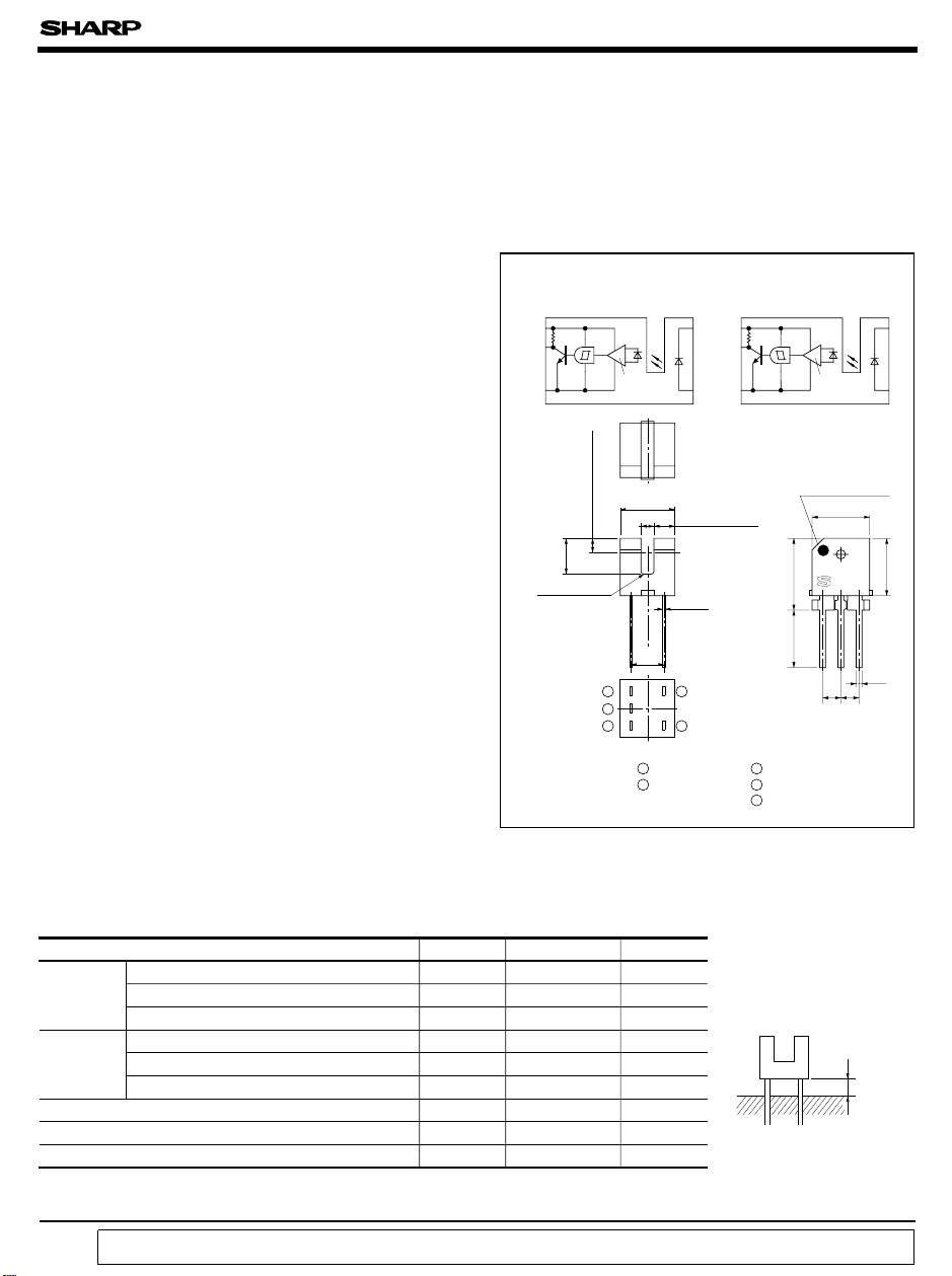
■ Outline Dimensions
Internal connection diagram
3
)
15kΩ
)
4
5
2 - C0.3
0.2
±
2.5
center
Detector
)
1.0
(
5
4
3
Amp.
3.8
0.9
❈
2.54
±
0.2
±
0.2
1.45
Optical
axis center
0.15
1
2
1 Anode
2 Cathode
213
±
4
5
0.2
(
Unit : mm
GP1A67HGP1A67L
(
)(
15kΩ
Amp.
Dot mark
(
GP1A67H
4.0
0.2
±
5.0
MIN.
4
❈❈
1.27 1.27
3 V
CC
4 V
out
5 GND
±
)
2
1
)
0.2
0.2
±
4.0
0.4
*“OPIC” (Optical IC) is a trademark of the SHARP Corporation.
An OPIC consists of a light-detecting element and signal processing circuit integrated onto a single chip.
* The dimensions indicated by ❈ refer to those measured from the lead base.
■ Absolute Maximum Ratings
(
Ta= 25˚C
)
Parameter Symbol Rating Unit
Input
Forward current I
Reverse voltage V
F
R
50 mA
6V
Power dissipation P 75 mW
Supply voltage
Output
Output current I
Power dissipation P
Operating temperature T
Storage temperature T
*1
Soldering temperature T
*1 For 5 seconds
“ In the absence of confirmation by device specification sheets, SHARP takes no responsibility for any defects that occur in equipment using any of SHARP's devices, shown in catalogs,
data books, etc. Contact SHARP in order to obtain the latest version of the device specification sheets before using any SHARP's device.”
V
CC
O
O
opr
stg
sol
7V
8mA
80 mW
- 25 to + 85 ˚C
- 40 to + 100 ˚C
260 ˚C
1mm or more
Soldering area
Page 2
GP1A67L/GP1A67H
■ Electro-optical Charcateristics
Parameter Symbol Conditions MIN. TYP. MAX. Unit
Input
Forward voltage
Reverse current I
Operating supply voltage
Low level
output voltage
High level
Output
output voltage
Low level
supply current
High level
supply current
“High→Low” threshold
*2
input current
“Low→High” threshold
*3
input current
*4
Hysteresis
Transfer
charac-
teristics
*2 I
FHL
*3 I
FLH
*4 Hysteresis stands for I
*5 Test circuit for response time shall be shown below.
“Low→High”
propagation delay
time
“High→Low”
propagation delay
time
Rise time
Response time
*5
Fall time
represents forward current when output changes from “ High” to “ Low” .
represents forward current when output changes from “ Low” to “ High” .
FLH/IFHL
GP1A67L
GP1A67H V
GP1A67L
GP1A67H V
GP1A67L
GP1A67H V
GP1A67L
GP1A67H V
GP1A67L I
GP1A67H I
GP1A67L
GP1A67H
GP1A67L
GP1A67H - 3.0 15
GP1A67L
GP1A67H - 9.0 30
(
GP1A67L) or I
Test Circuit for Response Time
= 7mA
I
F
Input
t
= t
= 0.01µ s
r
f
ZO= 50Ω
47Ω
Amp.
15kΩ
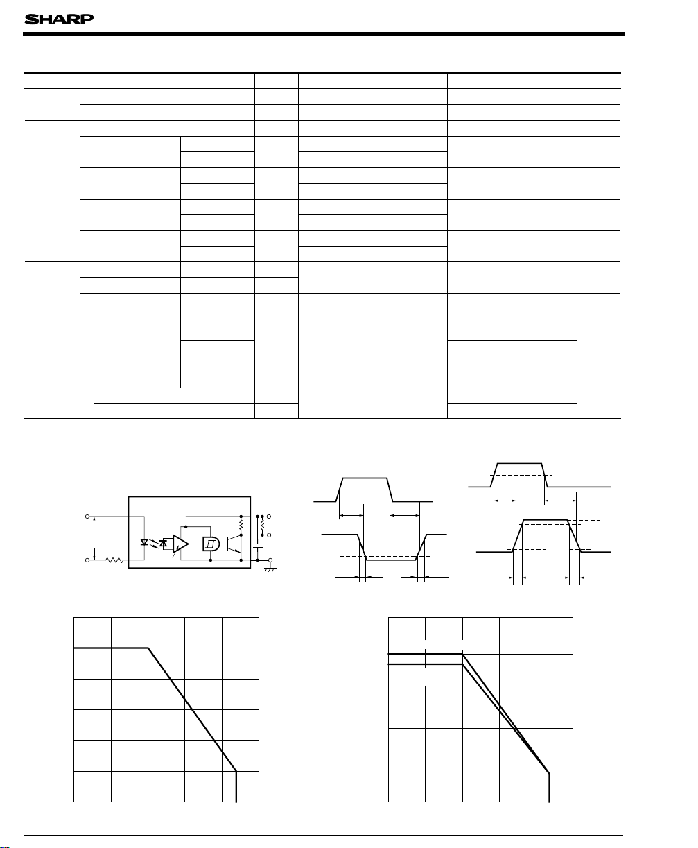
Fig. 1 Forward Current vs. Ambient
Temperature
60
V
R
V
CC
V
OL
V
OH
I
CCL
I
CCH
FHL
FLH
I
/I
FLH
I
FHL/IFLH
t
PLH
t
PHL
t
r
t - 0.05 0.5
f
(
/ I
GND
GP1A67H).
FLH
+ 5V
1.2kΩ
Output
0.1µ F
FHL
IF= 20mA - 1.2 1.4 V
F
VR=3V - - 10 µA
2.2 - 7.0 V
VCC= 5V, IOL= 4mA, IF= 5mA
= 5V, IOL= 4mA, IF=0
CC
= 5V, IF=0
V
CC
= 5V, IF= 5mA
CC
VCC= 5V, IF= 5mA
= 5V, IF=0
CC
VCC= 5V, IF=0
= 5V, IF= 5mA
CC
- 0.15 0.4 V
4.9 - - V
- 1.3 3.8 mA
- 1.0 3.0 mA
VCC= 5V - 0.9 2.5 mA
FHL
VCC= 5V 0.55 0.8 0.95 -
- 9.0 30
VCC=5V
= 5mA
I
F
= 1.2kΩ
R
L
GP1A67L
Input
Output
90%
10%
t
50%
t
PHL
r
t
PLH
- 3.0 15
- 0.1 0.5
GP1A67H
Input
Output
V
OH
1.5V
V
t
Output
OL
f
t
PLH
t
r
Fig. 2 Power Dissipation vs. Ambient
Temperature
100
(
Ta= 25˚C
50%
t
PHL
90%
10%
t
µ s
1.5V
f
)
8
V
OH
V
OL
50
)
mA
(
40
F
30
20
Forward current I
10
0
-25 -25
0
Ambient temperature Ta (˚C
)
100755025
Output power dissipation
)
80
mW
(
Input power
dissipation
60
40
Power dissipation P
20
0
0
25 50 75 100
Ambient temperature T
a
(˚C
)
Page 3

GP1A67L/GP1A67H
Fig. 3 Low Level Output Current vs.
Ambient Temperature
10
)
8
mA
(
OL
6
4
2
Low level output current I
0
-25 85
0
25 50 75 100
Ambient temperature Ta (˚C
)
Fig. 5 Relative Threshold Input Current vs.
Supply Voltage
1.2
FLH
1.0
, I
FHL
0.8
0.6
0.4
0.2
Relative threshold input current I
0
0
(
I
FHL
2.5
Supply voltage VCC (V
1
2
(
1 I
FHL
(
I
FLH
(
2 I
FLH
(
I
FHL
GP1A67L)&I
at VCC=5V
5 7.5 10
T
GP1A67L
GP1A67H
GP1A67L
GP1A67H
(
GP1A67H)=1
FLH
)
= 25˚C
a
)
)
)
)
Fig. 7 Low Level Output Voltage vs.
Low Level Output Current
1
0.5
)
V
(
OL
0.2
0.1
0.05
T
= 25˚C
a
V
Low level output voltage V
0.02
0.01
Low level output current IOL (mA
=5V
CC
= 5mA (GP1A67L
I
F
I
=0 (GP1A67H
F
)
)
502052
100101
)
Fig. 4 Forward Current vs. Forward Voltage
500
= 75˚C
T
)
mA
(
F
200
100
a
50˚C
50
25˚C
0˚C
- 25˚C
20
10
5
Forward current I
2
1
Forward voltage VF (V
)
3.50 0.5 1 1.5 2 2.5 3
Fig. 6 Relative Threshold Input Current vs.
Ambient Temperature
1.4
1I
(GP1A67L
FHL
I
(GP1A67H
FLH
2I
(GP1A67L
FLH
I
(GP1A67H
FHL
1.2
)
)
)
)
V
=5V
CC
1
1.0
2
0.8
Relative threshold input current
(
I
GP1A67L)&I
FHL
0.6
-25
at Ta= 25˚C
0
Ambient temperature Ta (˚C
(
GP1A67H)=1
FLH
)
100755025
Fig. 8 Low Level Output Voltage vs.
Ambient Temperature
0.5
V
=5V
CC
I
= 5mA (GP1A67L
F
I
=0 (GP1A67H
)
V
(
OL
F
0.4
0.3
0.2
0.1
Low level output voltage V
0
-25
0
Ambient temperature Ta (˚C
)
)
= 8mA
I
OL
4mA
1mA
25 50 75 100
)
Page 4

GP1A67L/GP1A67H
Fig. 9 Low Level Supply Current vs.
Supply Voltage
2.5
T
=- 25˚C
)
2.0
mA
(
CCL
1.5
1.0
0.5
Low level supply current I
0
010862
Supply voltage VCC (V
a
IF= 5mA (GP1A67L
I
=0 (GP1A67H
F
4
25˚C
85˚C
)
Fig.11 Propagation Delay Time vs.
Forward Current
12
)
10
µ s
(
PLH
8
, t
PHL
6
4
2
Propagation delay time t
0
0
10
Forward current I
1
VCC=5V
T
1t
2t
2
20 30
F
R
L
a
t
t
(mA
PLH
PHL
PHL
PLH
= 1.2kΩ
= 25˚C
(GP1A67L
(GP1A67H
(GP1A67L
(GP1A67H
)
)
)
)
)
)
)
40 50
Fig.10 High Level Supply Current vs.
Supply Voltage
2.5
)
2.0
mA
(
CCH
1.5
1.0
0.5
High level supply current I
0
268100
Supply voltage V
IF=0 (GP1A67L
I
4
Ta=- 25˚C
25˚C
85˚C
= 5mA (GP1A67H
F
)
(V
CC
Fig.12 Rise Time, Fall Time vs.
Load Resistance
0.7
VCC=5V
I
= 5mA
F
0.6
T
= 25˚C
a
)
µ s
0.5
(
f
, t
r
0.4
t
0.3
0.2
Rise time, fall time t
0.1
0
0.1
Load resistance RL (kΩ
r
t
f
110
)
)
)
100
■ Precautions for Use
(1)
In order to stabilize power supply line, connect a by-pass capacitor of more than 0.1µF bet-
ween Vcc and GND near the device.
(2)
Ultrasonic cleaning is prohibited.
(3)
As for other general cautions, refer to the chapter “Precautions for Use .”
 Loading...