

Page 1
GaAs MMICs GN8062
GN8062
GaAs IC
For semiconductor laser drive
■ Features
●
High-speed switching
●
High output
●
Pulse current and DC bias current can be controlled.
■ Absolute Maximum Ratings (Ta = 25˚C)
Parameter
Power supply voltage
Pin voltage
Power current
Output current
Allowable power dissipation
Channel temperature
Storage temperature
Operating ambient temperature
Symbol
V
DD
V
SS
V
IN
V
Ip
* 5
V
OUT
* 1
I
DD
* 4
I
SS
I
OUT
P
D
* 2
T
ch
T
stg
T
opr
* 3
Rating
6
– 6
– 0.5 to V
DD
–1.5
1.5 to V
DD
V
DD
50
40
145
700
150
– 55 to +150
–10 to +75
Unit
V
V
V
V
V
mA
mA
mA
mW
˚C
˚C
˚C
■ Electrical Characteristics (Ta = 25˚C)
Parameter
Pulse output current
Supply current
Input voltage
Rise time
Fall time
Test circuit
1
1
2
2
3
3
Condition
VDD= 5V, VSS= –5V, VIN= 2V, Ip=120mA, RL=10Ω
VDD= 5V, VSS= –5V, VIN= 0.4V, Ip=120mA, RL=10Ω
VDD= 5V, VSS= – 5V, VIN= 0.4V
I
p
= 0, RL=10Ω
VDD= 5V, VSS= – 5V, Ip=100mA
RL=10Ω
Min
100
2.5
Typ
120
1
35
25
Max
5
50
40
0.4
7
5
Unit
mA
mA
mA
mA
V
V
ns
ns
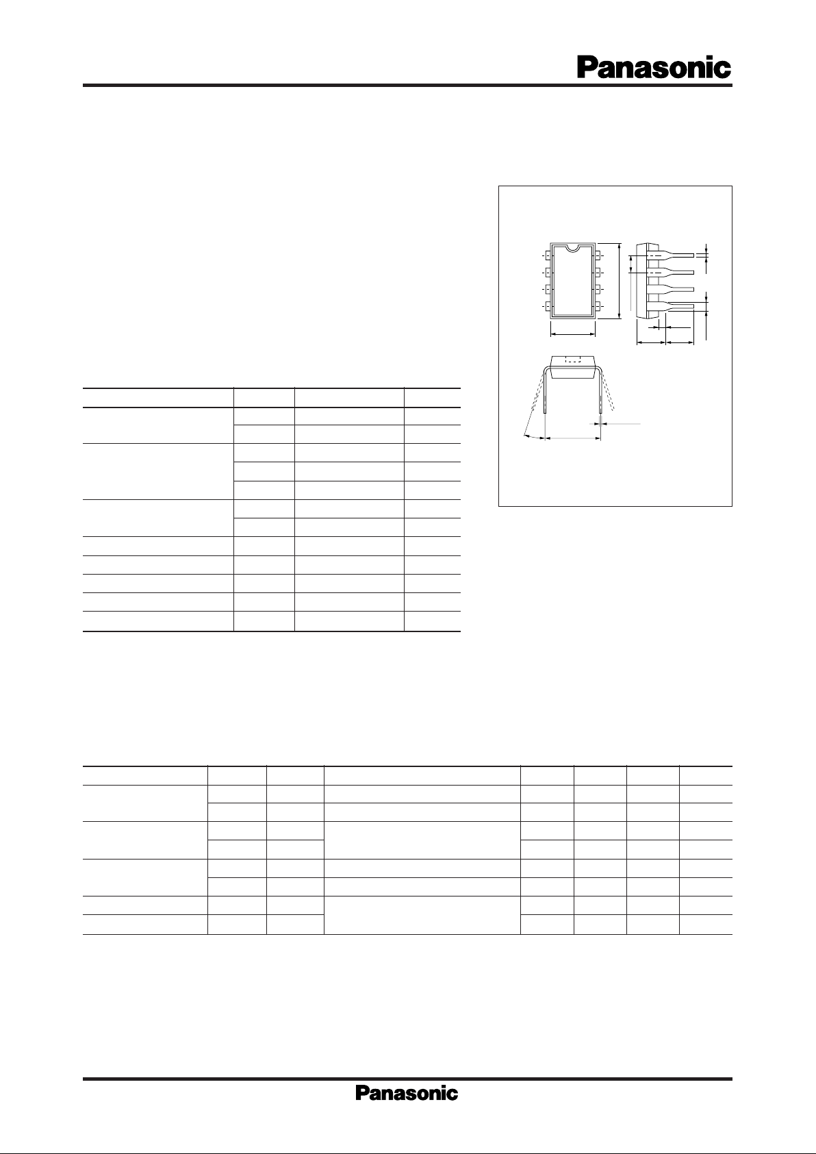
Unit : mm
1 : GND
2 : NC
3 : NC
4 : OUT
5 : V
IP
6 : V
DD
7 : V
IN
8 : V
SS
8-Lead Plastic DIL Package
* 1 Do not apply the voltage higher than the set VDD.
* 2 Guaranteed value of the unit at Ta= 25˚C.
* 3 Range in which the IC circuit function operates and not the guaranteed range of
electric characteristics.
* 4 IDD is a current when the pulse output current is zero.
* 5 Voltage when the constant current source has been connected.
Symbol
I
pmax.
I
pmin.
I
DD
* 1
I
SS
V
IH
V
IL
t
r
* 2
t
f
* 2
0.51.3typ.
4.0max.
0.7min.
4.5max.
0.35max.
6.4±0.2
7.62±0.2
2.54±0.25
10max.
0 to 15˚
1
2
3
4
8
7
6
5
Page 2
GaAs MMICs GN8062
* 1 The current value to be supplied from the 5V power supply is a total sum of this value plus the pulse output current and bias output current.
* 2 Waveform of input and output signals
Input signal
Output waveform
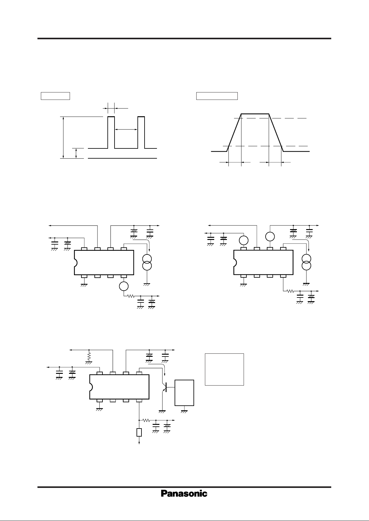
Test circuit 1 Test circuit 2
Test circuit 3
C1 : 0.1µF
C2 : 3.3µF
R1 : 10Ω
R2 : 50Ω
90%
t
f
t
r
10%
t
r ··· 10% to 90%
t
f ··· 90% to 10%
V
IN
I
P
=120mA
–5V
1234
8765
5V
C1 C2
–
+
C2
+
–
C2
R
L
C1
+
–
5V
C1
A
0.4V
I
P
=0mA
–5V
1234
8765
5V
C1 C2
–
+
C2
+
–
C2
R
L
C1
+
–
5V
C1
A
A
PULSE
GENERATOR
I
P
=100mA
–5V
1234
8765
5V
C1 C2
R2
–
+
C2
+
–
C2
R1
FET PROBE
C1
+
–
5V
C1
10µS
2
µS
2.5V min.
0.4V max.
*
The rise/fall time of the input signal
is 2ns (10 to 90%)
Page 3

GaAs MMICs GN8062
■ Block Diagram
■ Caution for Handling
1) The recommended VIN voltage is 2.5 to 3V for [H] and
0 to 0.4V for [L].
2) Do not apply VIN while the power supply is OFF.
3) For the current source to be connected to the VIP pin,
use a Si bipolar transistor as shown in the circuit diagram.
(Example: 2SD874)
To connect a resistor to the emitter or collector, use a
resistor of a few ohm. The use of higher resistor may
cause large change in the voltage at the VIP pin, and
may make the output waveform distortion. (See the pulse
output current control example).
To use another curr ent control circuit, set so that the V
IP
pin voltage becomes around 2V.
4) When mounting, minimize the connection distance be-
tween the semiconductor laser and IC, and use the chip
parts (C, R) of less parasitic effects.
5) Attention to damage by the power surge (see the ex-
ample connection of the pin protection circuit).
During handling, take care to ground the human body
and solder iron tip.
6) When the power supply is turned ON and OFF, set the
current value of the current source connected to the V
IP
pin to zero. This is important to prevent the large current flow through the semiconductor laser during power
ON/OFF.
When the power supply is ON, be sure to turn ON VDD,
after VSS is completely equal to – 5V. When the power
supply is OFF, be sure to turn OFF VSS, after VDD is
completely 0V.
7) Pay attention to release the heat.
Example of pulse output current control circuit
Connection example of pin protection circuit
V
IN
GND
NC
NC
OUT
OUT
1
2
3
4
8
7
6
5
V
SS
V
SS
V
SS
V
SS
V
SS
V
IN
V
DD
V
IP
V
DD
V
DD
V
IP
+
5V
LASER DIODE
OUTSIDE GN8062
INSIDE GN8062
from CONTROL
CIRCUIT
–5.0V
200Ω to 2kΩ 50Ω
5.0V
GN8062
MA3068(V
Z
=6.8V,Cd=85pF,RZ=6Ω)
GND
NC
NC
OUT
V
SS
V
IN
V
DD
V
IP
GND
NC
I
B
V
EE
=–
5 to 0V
I COLLECTOR
NC
OUT
V
SS
V
IN
V
DD
V
IP
5Ω
0.22mF
–
+
GN8062
 Loading...