

Page 1

DEC. 1998
Ver. 3.0
8-BIT SINGLE-CHIP MICROCONTROLLERS
GMS90 Series
DATA SHEET
Page 2

Version 3.0
Published by
MCU Application Team
1998 LG Semicon Co., Ltd. All right reserved.
Additional information of this manual may be served by LG Semicon offices in Korea or Distributo rs and Representatives listed at address directory.
LG Semicon reserves the right to make changes to any information here in at any time without notice.
The information, diagrams and other data in this manual are correct a nd reliable; however, LG Sem icon Co.,
Ltd. is in no way responsible for any viol ations of patents or oth er right s of the third party gene rated by the use
of this manual.
Page 3

GMS90 Series
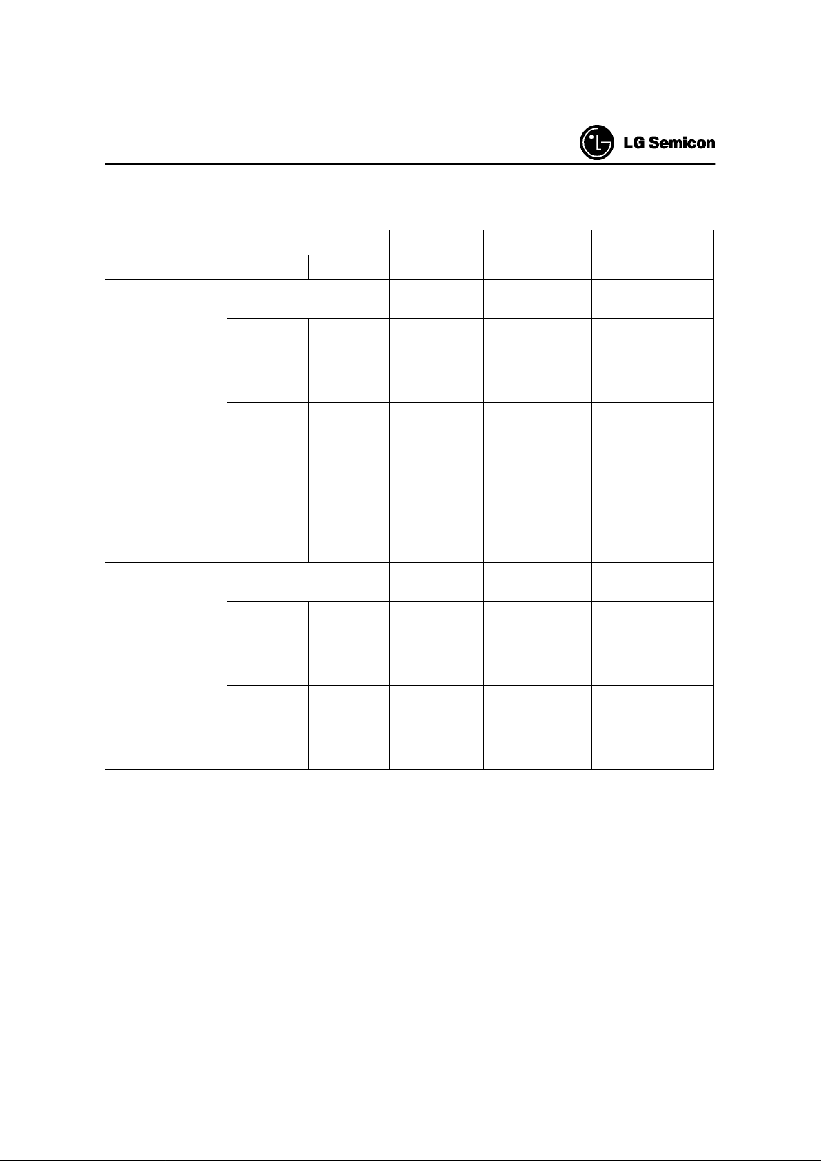
Device Naming Structure
GMS90X5X
LG Semicon MCU
Mask ROM version
GMS97X5X
- GBXXX XX XX
XXX
Frequency
Blank:
24:
40:
Package Type
Blank:
PL:
Q:
ROM Code serial No.
ROM size
1:
2:
4:
6:8:24k bytes
Operating Voltage
C:L:4.25~5.5V
12MHz
24MHz
40MHz
40PDIP
44PLCC
44MQFP
4k bytes
8k bytes
16k bytes
32k bytes
2.7~3.6V
OTP version
LG Semicon MCU
Dec. 1998 Ver 3.0
Package Type
Blank:
PL:
Q:
Frequency
Blank:H:12/24(5V),12MHz(3V)
ROM size
1:
2:
4:
6:8:24k bytes
Operating Voltage
C:L:4.25~5.5V
40PDIP
44PLCC
44MQFP
33MHz
4k bytes
8k bytes
16k bytes
32k bytes
2.7~3.6V
Page 4
GMS90 Series
GMS90 Series Selection Guide
Operating
Voltage
(V)
4.25~5.5
2.7~3.6
ROM size
MASK OTP
4K
8K
16K
24K
32K
-
-
-
-
-
-
-
-
-
-
4K
8K
16K
24K
32K
(bytes)
ROM-less
-
-
-
-
4K
4K
8K
8K
16K
16K
24K
24K
32K
32K
ROM-less
-
-
-
-
-
RAM size
(bytes)
128
256
128
256
256
256
256
128
128
256
256
256
256
256
256
256
256
128
256
128
256
256
256
256
Device Name
GMS90C31
GMS90C32
GMS90C51
GMS90C52
GMS90C54
GMS90C56
GMS90C58
GMS97C51
GMS97C51H
GMS97C52
GMS97C52H
GMS97C54
GMS97C54H
GMS97C56
GMS97C56H
GMS97C58
GMS97C58H
GMS90L31
GMS90L32
GMS90L51
GMS90L52
GMS90L54
GMS90L56
GMS90L58
Operating
Frequency
12/24/40
12/24/40
12/24/40
12/24/40
12/24/40
12/24/40
12/24/40
12/24
33
12/24
33
12/24
33
12/24
33
12/24
33
12/16
12/16
12/16
12/16
12/16
12/16
12/16
(MHz)
-
-
-
-
-
4K
8K
16K
24K
32K
128
256
256
256
256
GMS97L51
GMS97L52
GMS97L54
GMS97L56
GMS97L58
12
12
12
12
12
Note: The ROM version products in this data book will be applied to new masking version. (From Dec., 1998)
In case that you have old p roducts, please refer to previ ous data book (prior to this).
Dec. 1998 Ver 3.0
Page 5
GMS90 Series
GMS90C31/51, 97C51
GMS90L31/51, 97L51 (Low voltage versions)
• Fully compatible to standard MCS-51 microcontroller
• Wide operating frequency up to 40MHz (for more detail, see “GMS90 Series Selection Guide”)
•4K × 8 (EP)ROM
• 128 × 8 RAM
• 64K external program memory space
• 64K external data memory space
• Four 8-bit ports
• Two 16-bit Timers / Counters
• USART
• Five interrupt sources, two priority levels
• Power saving Idle and power down mode
• Quick pulse programming algorithm (in the OTP devices)
• 2-level program memory lock (in the OTP devices)
• 2.7Volt low voltage version available
• P-DIP-40, P-LCC-44, P-MQFP-44 package
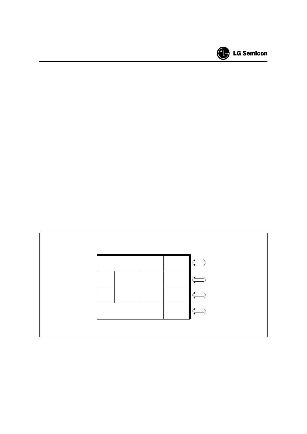
Block Diagram
128 × 8
T 0
T 1
ROM / EPROM
RAM
CPU
4K × 8
8-BIT
USART
PORT 0
PORT 1
PORT 2
PORT 3
I/O
I/O
I/O
I/O
Dec. 1998 Ver 3.0 1
Page 6
GMS90 Series
GMS90C32/52, 97C52
GMS90L32/52, 97L52 (Low voltage versions)
• Fully compatible to standard MCS-51 microcontroller
• Wide operating frequency up to 40MHz (for more detail, see “GMS90 Series Selection Guide”)
•8K × 8 (EP)ROM
• 256 × 8 RAM
• 64K external program memory space
• 64K external data memory space
• Four 8-bit ports
• Three 16-bit Timers / Counters (Timer2 with up/down counter feature)
• USART
• Six interrupt sources, two priority levels
• Power saving Idle and power down mode
• Quick pulse programming algorithm (in the OTP devices)
• 2-level program memory lock (in the OTP devices)
• 2.7Volt low voltage version available
• P-DIP-40, P-LCC-44, P-MQFP-44 package
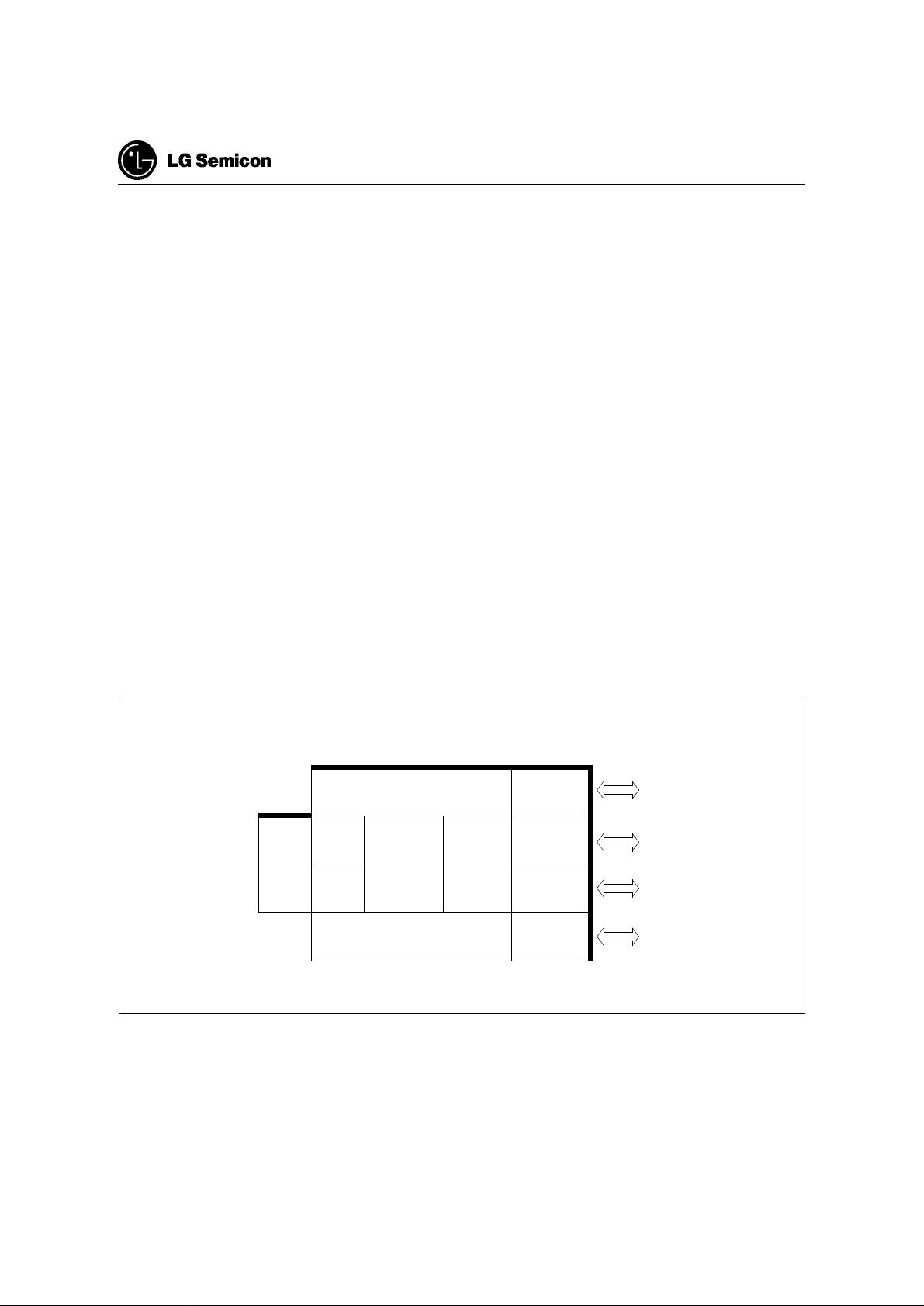
Block Diagram
T 2
T 0
T 1
ROM / EPROM
RAM
256 × 8
CPU
8K × 8
8-BIT
USART
PORT 0
PORT 1
PORT 2
PORT 3
I/O
I/O
I/O
I/O
2 Dec. 1998 Ver 3.0
Page 7
GMS90 Series
GMS90C54/56/58, 97C54/56/58
GMS90L54/56/58, 97L54/56/58 (Low voltage versions)
• Fully compatible to standard MCS-51 microcontroller
• Wide operating frequency up to 40MHz (for more detail, see “GMS90 Series Selection Guide”)
• 16K/24K/32K bytes (EP)ROM
• 256 × 8 RAM
• 64K external program memory space
• 64K external data memory space
• Four 8-bit ports
• Three 16-bit Timers / Counters (Timer2 with up/down counter feature)
• USART
• One clock output port
• Programmable ALE pin enable / disable
• Six interrupt sources, two priority levels
• Power saving Idle and power down mode
• Quick pulse programming algorithm (in the OTP devices)
• 2-level program memory lock (in the OTP devices)
• 2.7Volt low voltage version available
• P-DIP-40, P-LCC-44, P-MQFP-44 package
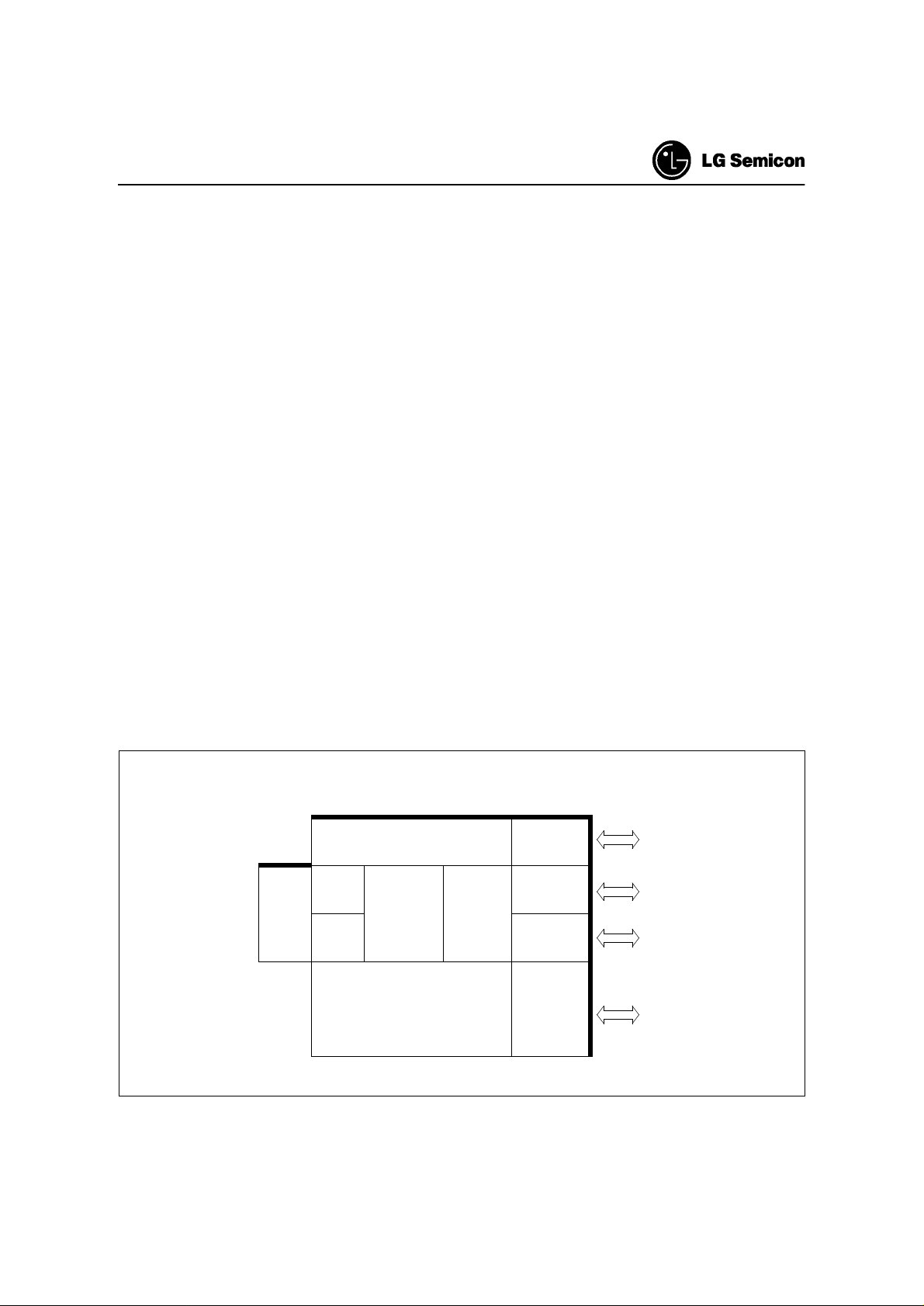
Block Diagram
T 2
RAM
256 × 8
T 0
CPU
T 1
ROM / EPROM
GMS9XX54: 16K × 8
GMS9XX56: 24K × 8
GMS9XX58: 32K × 8
8-BIT
USART
PORT 0
PORT 1
PORT 2
PORT 3
I/O
I/O
I/O
I/O
Dec. 1998 Ver 3.0 3
Page 8
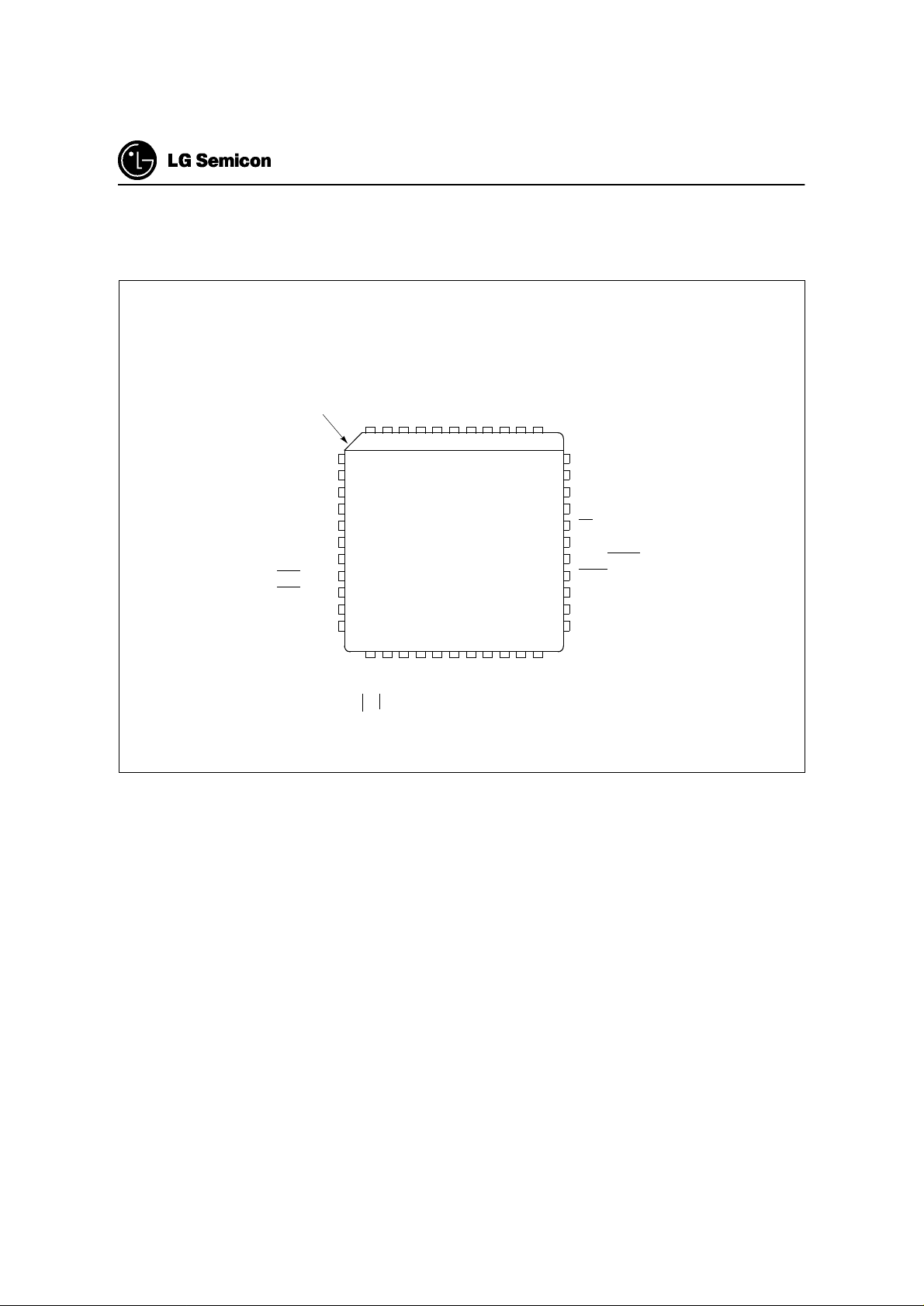
PIN CONFIGURATION
44-PLCC Pin Configuration (top view)
GMS90 Series
N.C.: Do not connect.
INDEX
CORNER
RESET
RxD / P3.0
N.C.*
TxD / P3.1
/ P3.2
INT0
/ P3.3
INT1
T0 / P3.4
T1 / P3.5
P1.5
P1.6
P1.7
P1.4
P1.3
P1.2
P1.1 / T2EX
65432
7
8
9
10
11
12
13
14
15
16
17
1819202122232425262728
/ P3.7
XTAL2
XTAL1
RD
WR / P3.6
P1.0 / T2
N.C.*
1
SS
V
N.C.*
CC
V
4443424140
P2.0 / A8
P0.0 / AD0
P2.1 / A9
P0.1 / AD1
P0.2 / AD2
P0.3 / AD3
P0.4 / AD4
39
P0.5 / AD5
38
P0.6 / AD6
37
P0.7 / AD7
36
/ V
EA
35
34
33
32
31
30
29
P2.2 / A10
P2.4 / A12
P2.3 / A11
PP
N.C.*
ALE / PROG
PSEN
P2.7 / A15
P2.6 / A14
P2.5 / A13
4 Dec. 1998 Ver 3.0
Page 9
GMS90 Series
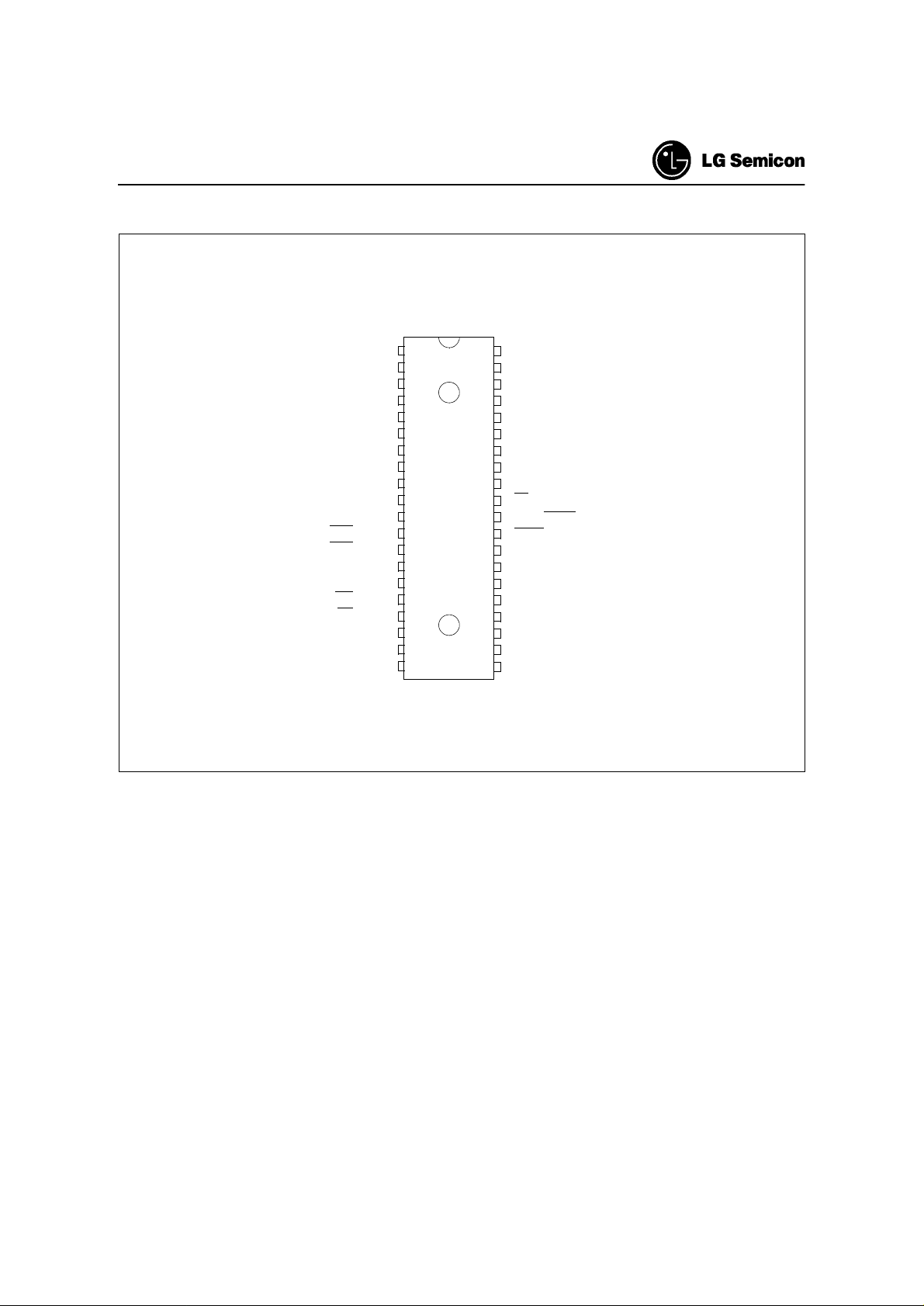
40-PDIP Pin Configuration (top view)
T2 / P1.0
T2EX / P1.1
P1.2
P1.3
P1.4
P1.5
P1.6
P1.7
RESET
RxD / P3.0
TxD / P3.1
/ P3.2
INT0
/ P3.3
INT1
T0 / P3.4
T1 / P3.5
/ P3.6
WR
/ P3.7
RD
XTAL2
XTAL1
V
V
1
2
3
4
5
6
7
8
9
10
11
12
13
14
15
16
17
18
19
SS
20
40
39
38
37
36
35
34
33
32
31
30
29
28
27
26
25
24
23
22
21
CC
P0.0 / AD0
P0.1 / AD1
P0.2 / AD2
P0.3 / AD3
P0.4 / AD4
P0.5 / AD5
P0.6 / AD6
P0.7 / AD7
/ V
EA
PP
ALE / PROG
PSEN
P2.7 / A15
P2.6 / A14
P2.5 / A13
P2.4 / A12
P2.3 / A11
P2.2 / A10
P2.1 / A9
P2.0 / A8
Dec. 1998 Ver 3.0 5
Page 10
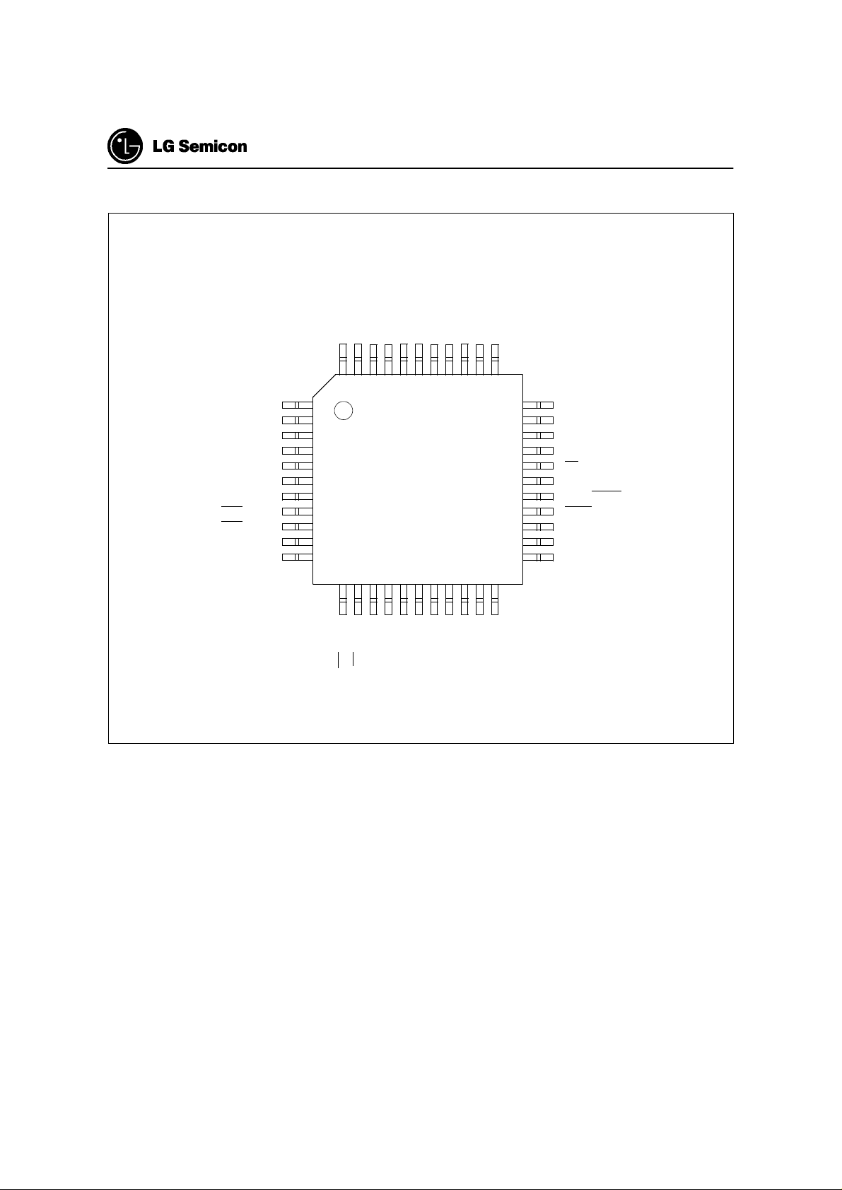
44-MQFP Pin Configuration (top view)
P1.4
4443424140393837363534
P1.5
P1.6
P1.7
RESET
RxD / P3.0
N.C.*
TxD / P3.1
/ P3.2
INT0
/ P3.3
INT1
T0 / P3.4
T1 / P3.5
1
2
3
4
5
6
7
8
9
10
11
1213141516171819202122
GMS90 Series
CC
P0.0 / AD0
P0.1 / AD1
P0.2 / AD2
P1.3
P1.2
P1.1 / T2EX
P1.0 / T2
N.C.*
V
P0.3 / AD3
33
32
31
30
29
28
27
26
25
24
23
P0.4 / AD4
P0.5 / AD5
P0.6 / AD6
P0.7 / AD7
/ V
EA
PP
N.C.*
ALE / PROG
PSEN
P2.7 / A15
P2.6 / A14
P2.5 / A13
N.C.: Do not connect.
SS
V
/ P3.7
XTAL2
RD
WR / P3.6
N.C.*
XTAL1
P2.0 / A8
P2.1 / A9
P2.2 / A10
P2.4 / A12
P2.3 / A11
6 Dec. 1998 Ver 3.0
Page 11
GMS90 Series
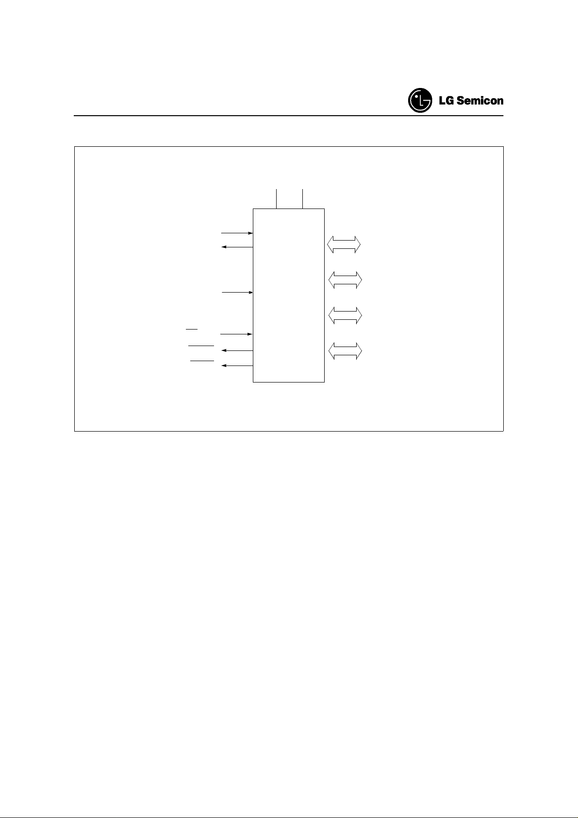
Logic Symbol
V
CCVSS
XTAL1
XTAL2
RESET
EA/V
PP
ALE/PROG
PSEN
Port 0
8-bit Digital I/O
Port 1
8-bit Digital I/O
Port 2
8-bit Digital I/O
Port 3
8-bit Digital I/O
Dec. 1998 Ver 3.0 7
Page 12
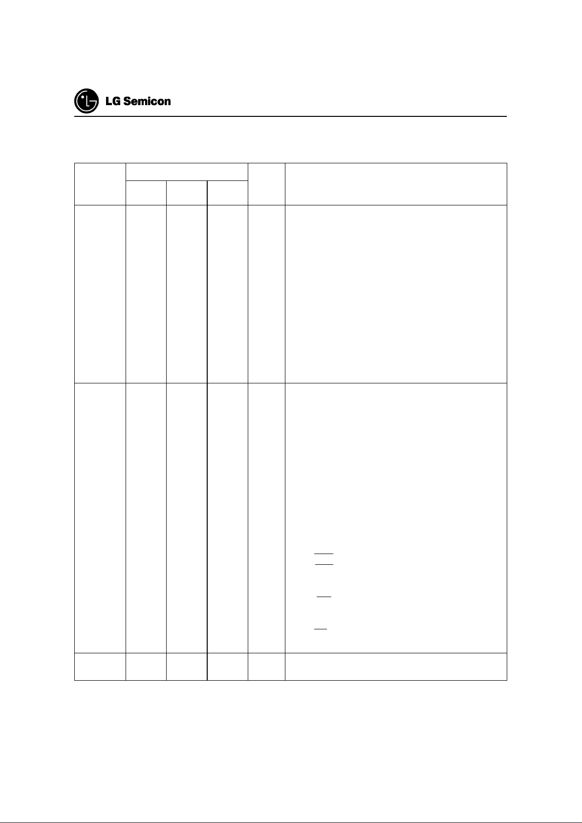
PIN DEFINITIONS AND FUNCTIONS
GMS90 Series
Symbol
P1.0-P1.7 2-9
P3.0-P3.7 11,
PLCC-44PDIP-40MQFP-
2
3
2
13-19
Pin Number
44
1-8
1
2
1
10-17 5, 7-13 I/O
40-44,
1-3
40
41
40
Input/
Output
I/O
Function
Port1
Port 1 is an 8-bit bidirectional I/O port with internal
pull-ups. Port 1 pins that have 1s written to them are
pulled high by the interna l pul l- up re si stor s a nd ca n b e
used as inputs. As inputs, port 1 pins that are
externally pulled low will source current because of
the pulls-ups (IIL, in the DC characteristics). Pins P1.0
and P1.1 also. Port1 also receives the low-order
address byte during program memory verification.
Port1 also serves alternate functions of Timer 2.
P1.0 / T2 : Timer/counter 2 external count input
P1.1 / T2EX : Timer/counter 2 trigger input
In GMS9XC54/56/58:
P1.0 / T2, Clock Out : Timer/counter 2 external count
input, Clock Out
Port 3
Port 3 is an 8-bit bidirectional I/O port with internal
pull-ups. Port 3 pins that have 1s written to them are
pulled high by the interna l pul l- up re si stor s a nd ca n b e
used as inputs. As inputs, port 3 pins that are
externally pulled low will source current because of
the pulls-ups (IIL, in the DC characteristics). Port 3 also
serves the special features of the 80C51 family, as
listed below.
11
13
14
15
16
17
18
19
XTAL2 20 18 14 O
10
11
12
13
14
15
16
17
10
11
12
13
5
7
8
9
P3.0 / RxD
P3.1 / TxD
P3.2 /INT0
P 3 .3 / INT 1
P3.4 /T0
P3.5 /T1
P3.6 / WR
P3.7 /RD
XTAL2
Output of the inverting oscillator amplifier.
receiver data input (asynchronous) or
data input output(synch rono us) of serial
interface 0
transmitter data output (asynchronous)
or clock output (synchronous) of the
serial interface 0
interrupt 0 input/timer 0 gate control
interrupt 1 input/timer 1 gate control
counter 0 input
counter 1 input
the write control signal latches the data
byte from port 0 into the external data
memory
the read control signal enables the
external data memory to port 0
8 Dec. 1998 Ver 3.0
Page 13
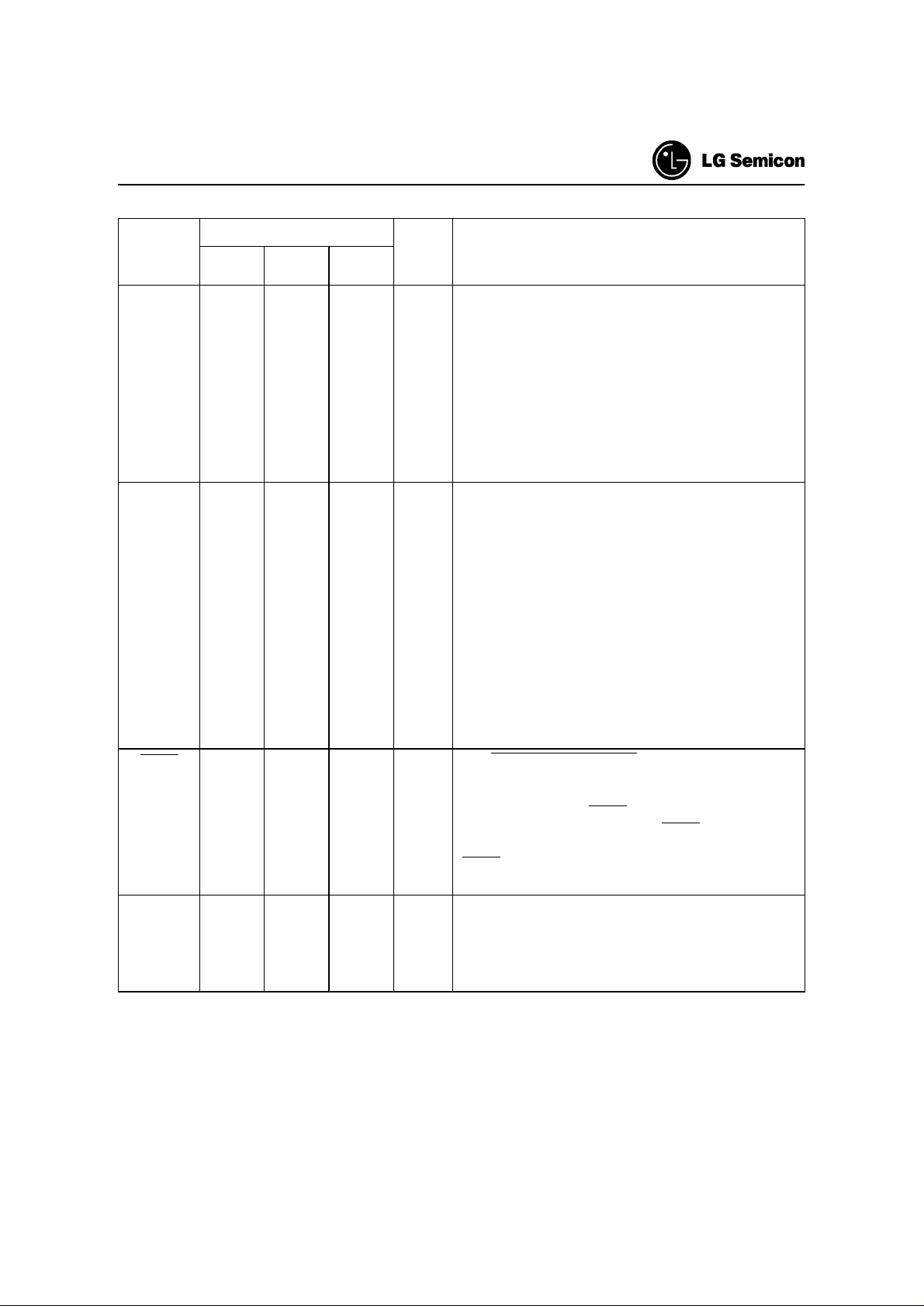
GMS90 Series
Pin Number
Symbol
XTAL1 21 19 15 I
P2.0-P2.7 24-31 21-28 18-25 I/O
PSEN 32 29 26 O
RESET 10 9 4 I
PLCC-44PDIP-40MQFP-
44
Input/
Output
Function
XTAL1
Input to the inverting oscillator amplifier and input to
the internal clock generator circuits.To drive the
device from an external clock source, XTAL1 should
be driven, while XTA L2 is le ft un con nec ted . There are
no requirements on the duty cycle of the external
clock signal, since the input to the internal clocking
circuitry is divided down by a divide-by-two flip-flop.
Minimum and maximum high an d low times as well as
rise fall times specified in the AC characteristics must
be observed.
Port 2
Port 2 is an 8-bit bidirectional I/O port with internal
pull-ups. Port 2 pins that have 1s written to them are
pulled high by the internal pull-up resistors and can be
used as inputs. As inputs, port 2 pins that are
externally pulled low will source current because of
the pulls-ups (IIL, in the DC characteristics).Port 2
emits the high-order addr ess by te d uring fetch es fro m
external program memory and during accesses to
external data memory that use 16-bit addresses
(MOVX @DPTR). In this application it uses strong
internal pull-ups when emitting 1s. During accesses to
external data memory that use 8-bit addresses
(MOVX @Ri), port 2 emits the contents of the P2
special function register.
The Program Store Enable
The read strobe to external program memory when
the device is executing code from the external
program memory. PSEN is activated twice each
machine cycle, except that two PSEN activations are
skipped during each access to external data memory.
PSEN is not activated during fetches from internal
program memory.
RESET
A high level on this pin for two machine cycles while
the oscillator is running resets the device. An inter nal
diffused resistor to VSS permits power-on reset us ing
only an external capaci tor to VCC.
Dec. 1998 Ver 3.0 9
Page 14
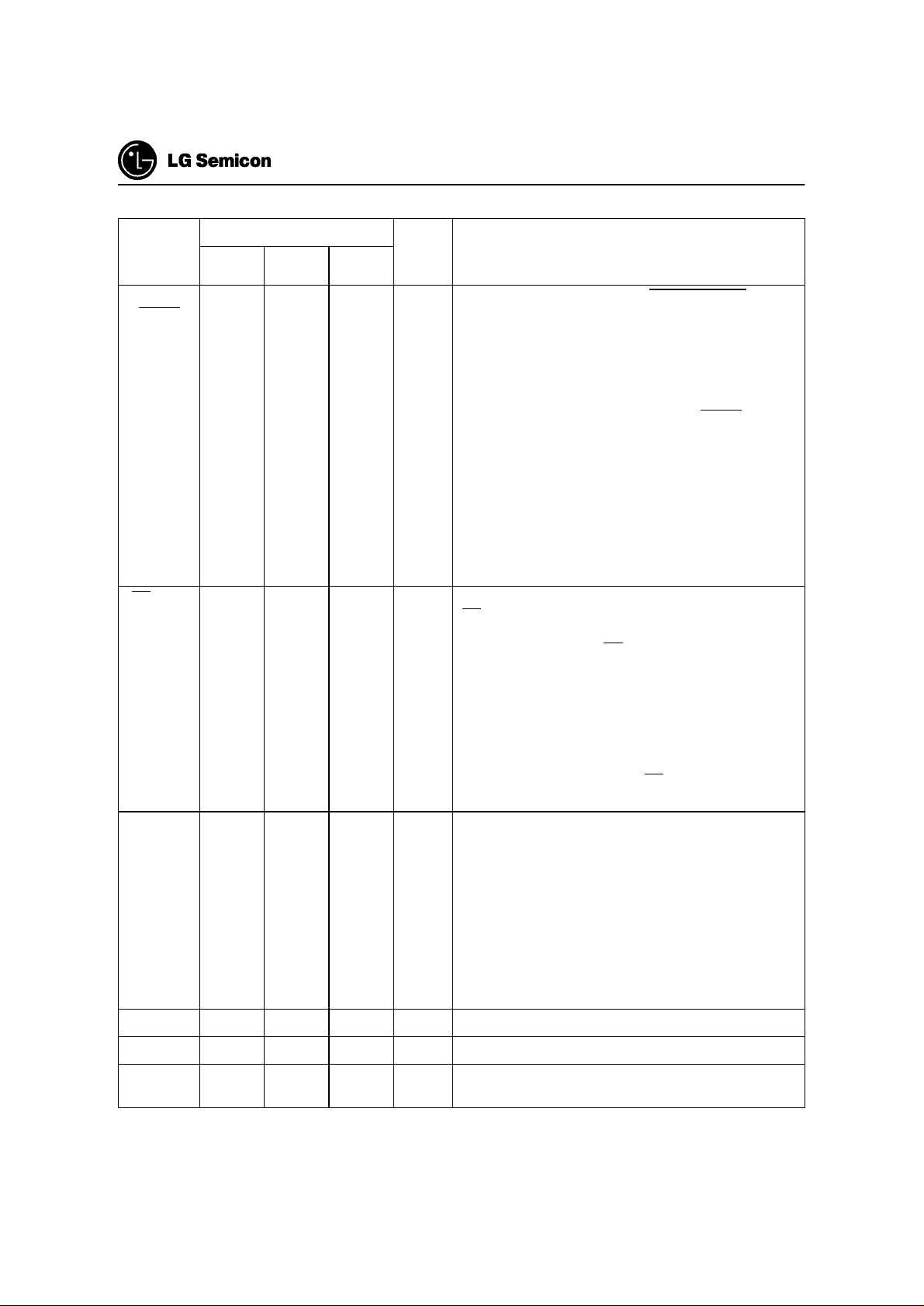
GMS90 Series
Symbol
ALE /
PROG
EA / V
Pin Number
PLCC-44PDIP-40MQFP-
33 30 27 O
PP
35 31 29 I External Access Enable / Program Supply Voltage
44
Input/
Output
Function
The Address Latch Enable / Program pulse
Output pulse for latching the low byte of the address
during an access to external memory. In normal
operation, ALE is emitted at a constant rate of 1/6 the
oscillator frequency, and can be used for external
timing or clocking. Note that one ALE pulse is skipped
during each access to external data memor y. This pin
is also the program pulse input (PROG) during
EPROM programming.
In GMS9XC54/56/58:
If desired, ALE operation can be disabled by setting
bit 0 of SFR locat ion 8EH. With this bit set, the pin is
weakly pulled high. The ALE disable feature will be
terminated by reset. Setting the ALE-disable bit has
no affect if the microcont roller is in ex ternal execut ion
mode.
EA must be external held low to enable the device to
fetch code from external program memory locations
0000H to FFFFH. If EA is held high, the device
executes from internal program memory unless the
program counter contai ns an address greater than its
internal memory size. This pin also receives the
12.75V programming supply voltage (VPP) during
EPROM programming.
Note; however, that if any of the Lock bits are
programmed, EA will be internally
latched on reset.
P0.0-P0.7 36-43 32-39 30-37 I/O
Port 0
Port 0 is an 8-bit open-drain bidirectional I/O port.
Port 0 pins that have 1s wri tten to them f loat and can
be used as high-impedan ce inputs.
Port 0 is also the multiplexed low-order address and
data bus during accesses to external program and
data memory. In this application it uses strong internal
pull-ups when emitting 1s. Port 0 also outputs the
code bytes during program verification in the
GMS97X5X. External pull-up resistors are required
during program verification.
V
SS
V
CC
N.C. 1,12
22 20 16 44 40 38 -
-6,17
23,34
28,39
Circuit ground potential
Supply terminal
-
No connection
for all operating modes
10 Dec. 1998 Ver 3.0
Page 15
GMS90 Series
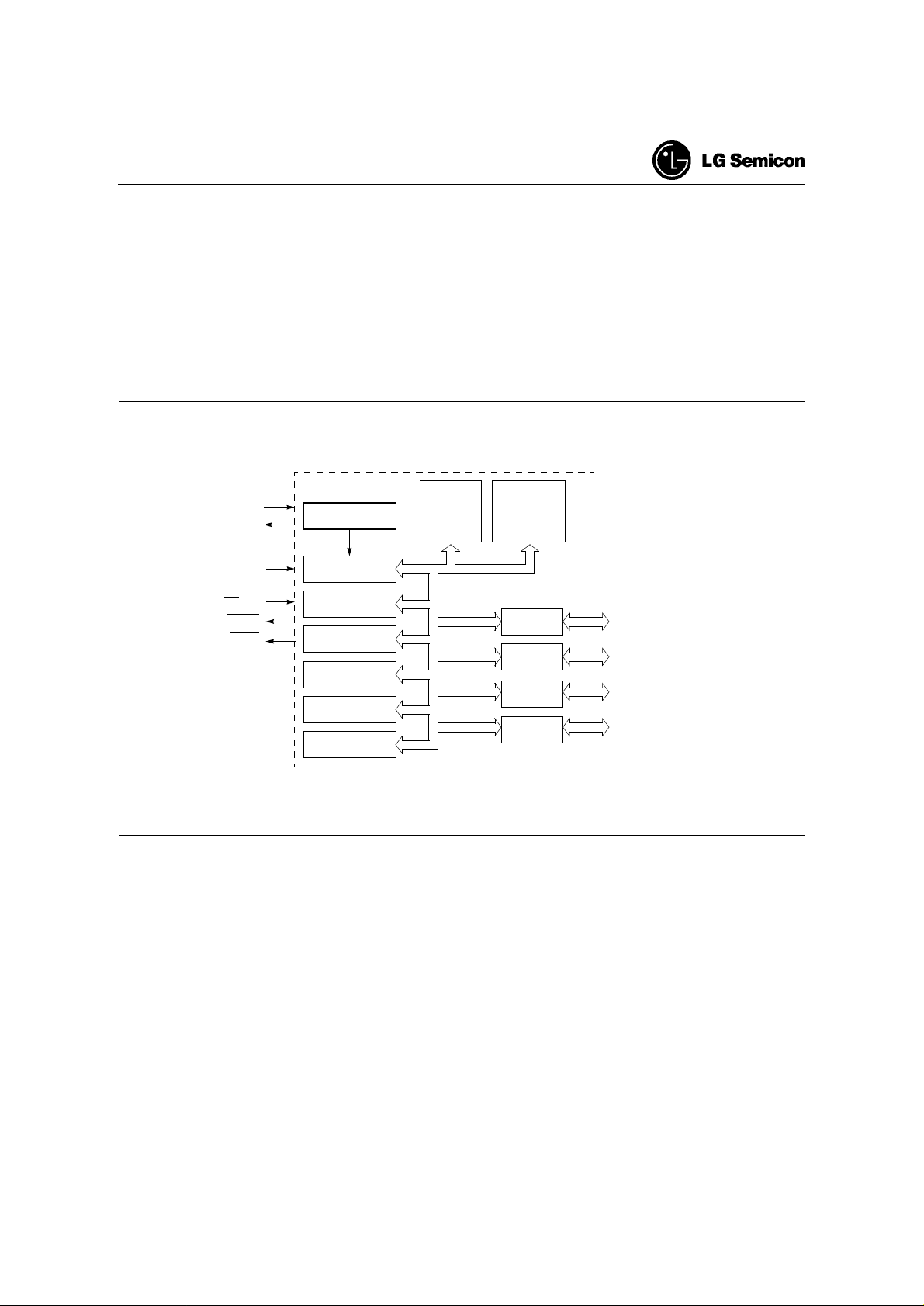
FUNCTIONAL DESCRIPTION
The GMS90 series is fully compatible to the standard 8051 microcontroller family.
It is compatible with the general 8051 family. While maintaining all architectural and operational characteristics
of the general 8051 family.
Figure 1 shows a block diagram of the GMS90 series
XTAL1
XTAL2
RESET
/V
EA
ALE/PROG
PSEN
PP
OSC & TIMING
CPU
Timer 0
Timer 1
Timer 2
Interrupt Unit
Serial Channel
Figure 1. Block Diagram of the GMS90 series
RAM
128/256×8
ROM/EPROM
4K/8K/16K
24K/32K
Port 0
Port 1
Port 2
Port 3
Port 0
8-bit Digit. I/O
Port 1
8-bit Digit. I/O
Port 2
8-bit Digit. I/O
Port 3
8-bit Digit. I/O
Dec. 1998 Ver 3.0 11
Page 16
GMS90 Series
CPU
The GMS90 series is efficient both as a controller and as an arithmetic processor. It has extensive facilities for
binary and BCD arithmetic and excels in its bit-handling capabilities. Efficient use of program memory results
from an instruction set consisting of 44% one-byte, 41% two-byte, and 15% three-byte instructions. With a 12
MHz crystal, 58% of the instructions are executed in 1.0µs (40MHz: 300ns).
Special Function Register PSW
LSB
PSW
Bit No.
Addr. D0
MSB
76543210
H
CY AC F0 RS1 RS0 OV F1 P
Bit Function
Carry Flag
Auxiliary Carry Flag
(for BCD operations)
General Purpose Flag
Register Bank select control bits
Bank 0 selected, data address 00H - 07
Bank 1 selected, data address 08H - 0F
Bank 2 selected, data address 10H - 17
Bank 3 selected, data address 18H - 1F
H
H
H
H
Overflow Flag
General Purpose Flag
Parity Flag
Set/cleared by hardware each instruction cycle to indicate an odd/even
number of "one" bits in the accumulator, i.e. ev en parity.
RS1
0
0
1
1
CY
AC
F0
RS0
0
1
0
1
OV
F1
P
Reset value of PSW is 00H.
12 Dec. 1998 Ver 3.0
Page 17
GMS90 Series
SPECIAL FUNCTION REGISTERS
All registers, except the progra m coun ter and th e four ge neral purp ose regi ster bank s, resi de in the s pecial fun ction register area.
The 28 special function registers (SFR) include pointers and registers that provide an interface between the CPU
and the other on-chip peripherals. There are also 128 directly addressable bits within the SFR area.
All SFRs are listed in Table 1, Table 1, and Table 3.
In Table 1 they are organized in nume ric order of their addr esses. In Tabl e 2 they are organ ized in groups wh ich
refer to the functional blocks of the GMS90 series. Table 3 illustrates the contents of the SFRs.
Table 1. Special Function Registers in Numeric Order of their Addresses
Address Register
80H
81H
82H
83H
84H
85H
86H
87H
88H
89H
8AH
8BH
8CH
8DH
3)
8EH
8FH
1) Bit-addressable Special Function Regis ter.
2) X means that the value is indeterminate and the location is reserved.
3) The GMS9XX54/56/58 have the AUXR0 reg iste r at ad dr ess 8EH.
1)
P0
SP
DPL
DPH
reserved
reserved
reserved
PCON
1)
TCON
TMOD
TL0
TL1
TH0
TH1
3)
☞
reserved
Contents after
Reset
FFH
07H
00H
00H
2)
XXH
2)
XXH
2)
XXH
0XX0000
2)
B
00H
00H
00H
00H
00H
00H
3)
☞
2)
XXH
Address Register
90H
91H
92H
93H
94H
95H
96H
97H
98H
99H
9AH
9BH
9CH
9DH
9EH
9FH
GMS9XX51/52 GMS9XX54/56/58
8E
H
reserved XXXXXXX0
XXXXXXXX
2)
B
8E
H
1)
P1
reserved
reserved
reserved
reserved
reserved
reserved
reserved
SCON
SBUF
reserved
reserved
reserved
reserved
reserved
reserved
AUXR0
1)
Contents after
Reset
FF
00
XXH
XXH
XXH
XXH
XXH
XXH
00H
XXH
XXH
XXH
XXH
XXH
XXH
XXH
H
H
2)
2)
2)
2)
2)
2)
2)
2)
2)
2)
2)
2)
2)
2)
B
Dec. 1998 Ver 3.0 13
Page 18
GMS90 Series
Table 1. Special Function Registers in Numeric Order of their Addresses
Address Register
A0H
A1H
A2H
A3H
A4H
A5H
A6H
A7H
A8H
A9H
AAH
ABH
ACH
ADH
AEH
AFH
B0H
B1H
B2H
B3H
B4H
B5H
B6H
B7H
B8H
B9H
BAH
BBH
BCH
BDH
BEH
BFH
C0H
C1H
C2H
C3H
C4H
C5H
C6H
C7H
1)
P2
reserved
reserved
reserved
reserved
reserved
reserved
reserved
1)
IE
reserved
reserved
reserved
reserved
reserved
reserved
reserved
1)
P3
reserved
reserved
reserved
reserved
reserved
reserved
reserved
1)
IP
reserved
reserved
reserved
reserved
reserved
reserved
reserved
reserved
reserved
reserved
reserved
reserved
reserved
reserved
reserved
Contents after
Reset
FFH
2)
XXH
2)
XXH
2)
XXH
2)
XXH
2)
XXH
2)
XXH
2)
XXH
0X000000B
2)
XXH
2)
XXH
2)
XXH
2)
XXH
2)
XXH
2)
XXH
2)
XXH
FFH
2)
XXH
2)
XXH
2)
XXH
2)
XXH
2)
XXH
2)
XXH
2)
XXH
XX000000B
2)
XXH
2)
XXH
2)
XXH
2)
XXH
2)
XXH
2)
XXH
2)
XXH
XX
H
2)
XXH
2)
XXH
2)
XXH
2)
XXH
2)
XXH
2)
XXH
2)
XXH
2)
2)
Address Register
C8H
3)
C9H
CAH
CBH
CCH
CDH
CEH
CFH
D0H
D1H
D2H
D3H
D4H
D5H
D6H
D7H
D8H
D9H
DAH
DBH
DCH
DDH
DEH
DFH
E0H
E1H
E2H
E3H
E4H
E5H
E6H
E7H
E8H
E9H
EAH
EBH
ECH
EDH
EEH
EFH
(cont’d)
T2CON
T2MOD
RC2L
RC2H
TL2
TH2
reserved
reserved
PSW
reserved
reserved
reserved
reserved
reserved
reserved
reserved
reserved
reserved
reserved
reserved
reserved
reserved
reserved
reserved
ACC
reserved
reserved
reserved
reserved
reserved
reserved
reserved
reserved
reserved
reserved
reserved
reserved
reserved
reserved
reserved
1)
1)
1)
Contents after
Reset
00H
3)
☞
00H
00H
00H
00H
2)
XXH
2)
XXH
00H
2)
XXH
2)
XXH
2)
XXH
2)
XXH
2)
XXH
2)
XXH
2)
XXH
2)
XXH
2)
XXH
2)
XXH
2)
XXH
2)
XXH
2)
XXH
2)
XXH
2)
XXH
00H
2)
XXH
2)
XXH
2)
XXH
2)
XXH
2)
XXH
2)
XXH
2)
XXH
2)
XXH
2)
XXH
2)
XXH
2)
XXH
2)
XXH
2)
XXH
2)
XXH
2)
XXH
14 Dec. 1998 Ver 3.0
Page 19
GMS90 Series
Table 1. Special Function Registers in Numeric Order of their Addresses
Address Register
F0H
F1H
F2H
F3H
F4H
F5H
F6H
F7H
1) Bit-addressable Special Function Regis ter.
2) X means that the value is indeterminate and the location is reserved.
3) Address C9
is configured as below.
H
1)
B
reserved
reserved
reserved
reserved
reserved
reserved
reserved
Contents after
Reset
00H
2)
XXH
2)
XXH
2)
XXH
2)
XXH
2)
XXH
2)
XXH
2)
XXH
Address Register
F8H
F9H
FAH
FBH
FCH
FDH
FEH
FFH
GMS9XX51/52 GMS9XX54/56/58
C9
H
reserved XXXXXX00
XXXXXXX0
2)
B
C9
H
(cont’d)
reserved
reserved
reserved
reserved
reserved
reserved
reserved
reserved
T2MOD
Contents after
Reset
2)
XXH
2)
XXH
2)
XXH
2)
XXH
2)
XXH
2)
XXH
2)
XXH
2)
XXH
2)
B
Dec. 1998 Ver 3.0 15
Page 20
Table 2. Special Function Registers - Functional Blocks
GMS90 Series
Block Symbol Name Address
CPU ACC
B
DPH
DPL
PSW
SP
Interrupt System IE
IP
Ports P0
P1
P2
P3
Serial Channels
PCON
SBUF
SCON
Timer 0/ Timer 1 TCON
TH0
TH1
TL0
TL1
TMOD
Accumulator
B-Register
Data Pointer, High Byte
Data Pointer, Low Byte
Program Status Word Register
Stack Pointer
Interrupt Enable Register
Interrupt Priority Register
Port 0
Port 1
Port 2
Port 3
3)
Power Control Register
Serial Channel Buffer Reg.
Serial Channel 0 Control Reg.
Timer 0/1 Control Register
Timer 0, High Byte
Timer 1, High Byte
Timer 0, Low Byte
Timer 1, Low Byte
Timer Mode Register
E0H
F0H
83H
82H
D0H
81H
A8H
B8H
80H
90H
A0H
B0H
87H
99H
98H
88H
8CH
8DH
8AH
8BH
89H
1)
1)
1)
1)
1)
1)
1)
1)
1)
1)
1)
Contents
after Reset
00H
00H
00H
00H
00H
07H
0X000000B
XX000000B
FFH
FFH
FFH
FFH
0XXX0000B
2)
XXH
00H
00H
00H
00H
00H
00H
00H
2)
2)
2)
Timer 2 T2CON
T2MOD
RC2H
RC2L
TH2
TL2
AUXR0
Power Saving
PCON
Timer 2 Control Register
Timer 2 Mode Register
Timer 2 Reload Capture Reg., High Byte
Timer 2 Reload Capture Reg., Low Byte
Timer 2, High Byte
Timer 2, Low Byte
4)
Aux. Register 0
3)
Power Control Register 87H
C8H
C9H
CBH
CAH
CDH
CCH
8EH
1)
00H
00H
00H
00H
00H
00H
XXXXXXX0B
0XXX0000B
2)
2)
Modes
1) Bit-addressable Special Function regi ster
2) X means that the value is indeterminate and the location is reserved
3) This special function register is listed repeatedly since some bit of it also belong to other functional block s
4) The AUXR0 is in the GMS9XX54/56/58 only.
16 Dec. 1998 Ver 3.0
Page 21
GMS90 Series
Table 3. Contents of SFRs, SFRs in Numeric Order
Address Register
Bit 76543210
80H P0
81H SP
82H DPL
83H DPH
87H PCON
SMOD
---GF1GF0PDEIDLE
88H TCON TF1 TR1 TF0 TR0 IE1 IT1 IE0 IT0
89H TMOD GATE C/T M1 MT GATE C/T M1 M0
8AH TL0
8BH TL1
8CH TH0
8DH TH1
8EH
AUXR0
†
-------
90H P1
A0
†
98H SCON SM0 SM1 SM2 REN TB8 RB8 TI RI
99H SBUF
A0H P2
A8H IE EA - ET2 ES ET1 EX1 ET0 EX0
B0H P3
B8H IP - - PT2 PS PT1 PX1 PT0 PX0
† indicates resident in the GMS9XX54/56/58, not in 9XX51/52.
SFR bit and byte addres sable
SFR not bit addressabl e
- : this bit location is reserved
Dec. 1998 Ver 3.0 17
Page 22
GMS90 Series
Table 3. Contents of SFRs, SFRs in Numeric Order
Address Register
Bit 76543210
C8H T2CON TF2 EXF2 RCLK TCLK
(cont’d)
EXEN2
C9HT2MOD ------
CAH RC2L
CBH RC2H
CCH TL2
CDH TH2
D0H PSW CY AC F0 RS1 RS0 OV
E0H ACC
F0H B
† indicates resident in the GMS9XX54/56/58, not in 9XX51/52.
SFR bit and byte addressable
TR2 C/T2
T2OE
F1
†
CP/RL2
DCEN
P
SFR not bit addressabl e
- : this bit location is reserved
18 Dec. 1998 Ver 3.0
Page 23
GMS90 Series
TIMER / COUNTER 0 AND 1
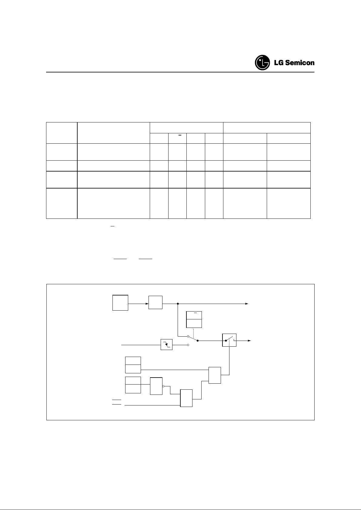
Timer/Counter 0 and 1 can be used in four operating modes as listed in Table 4:
Table 4. Timer/Counter 0 and 1 Operating Modes
Mode Description
TMOD Input Clock
Gate C/T M1 M0 internal external (Max.)
0
8-bit timer/counter with a
divide-by-32 prescaler
XX00
1 16-bit timer/counter X X 0 1
2
8-bit timer/counter with
8-bit auto-reload
XX10
f
÷(12×32) f
OSC
f
÷12 f
OSC
f
÷12 f
OSC
OSC
OSC
OSC
÷(24×32)
÷24
÷24
Timer/counter 0 used as
3
one 8-bit timer/counter and
one 8-bit timer Timer 1
XX11
f
÷12 f
OSC
OSC
÷24
stops
In the "timer" function (C/T
f
/12.
OSC
= "0") the register is incremented every machine cycle. Therefore the count rate is
In the "counter" function the register is incremented in response to a 1-to-0 transition at its corresponding ext ernal input pin (P3.4/T0, P3.5/T1) . Since it takes two machine cycles to detect a falling edge the max. count rate
/24. External inputs INT0 and INT1 (P3.2, P3.3) can be programmed to function as a gate to facilitate
is f
OSC
pulse width measurements. Figure 2 illustrates the input clock logic.
12
f
OSC
÷
f
OSC
12
÷
C/T
TMOD
0
P3.4/T0
P3.5/T1
f
Max.
OSC
P3.2 / INT0
P3.3 / INT1
/24
TR0 / 1
TCON
Gate
TMOD
=1
1
&
1
≥
Timer 0/1
Input Clock
Figure 2. Timer/Counter 0 and 1 Input Clock Logic
Dec. 1998 Ver 3.0 19
Page 24
GMS90 Series
TIMER 2
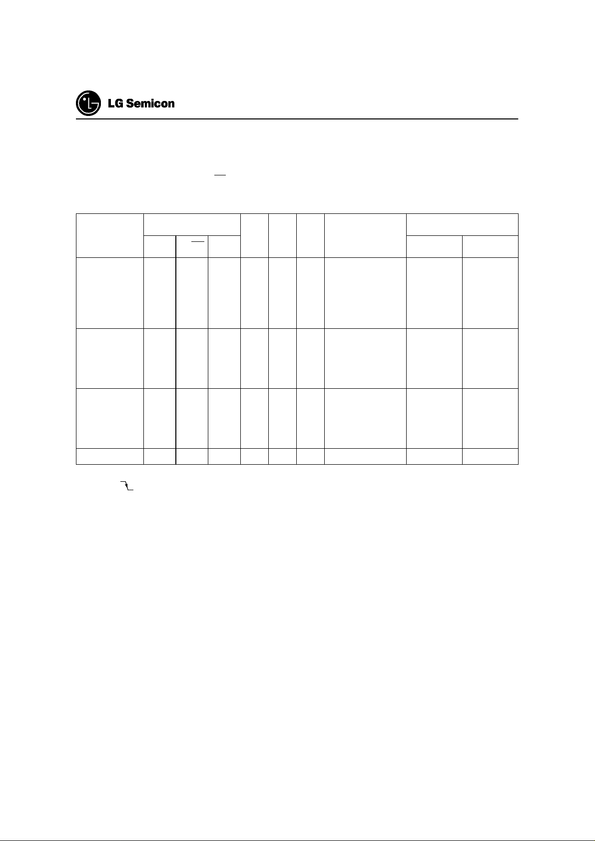
Timer 2 is a 16-bit timer/Counter with an up/do wn count feature. It can o perate either as timer o r as an event
counter which is selected by bit C/T2
Table 5. Timer/Counter 2 Operating Modes
(T2CON.1). It has three operating modes as shown in Table 5.
T2MO
T2CON
D
TR2 DCEN EXEN2 internal
1
0
P1.1/
T2EX
0
X
Remarks
reload upon over-
Input Clock
flow
1
1
1
1
0
1
1
X
↓
1
reload trigger (falling edge)
X
0
Down counting
X
1
Up counting
0
X↓16 bit Timer/ Coun-
f
OSC
÷ 12
ter (only up-count-
f
ing)
1
X
1
capture TH2,TL2
OSC
÷ 12
external
(P1.0/T2)
f
OSC
f
OSC
Mode
16-bit AutoReload
16-bit
Capture
RCLK or
TCLK
0
0
0
0
0
0
T2CON
CP/RL2
0
0
0
0
1
1
→ RC2H,RC2L
Baud Rate
Generator
1
X
1
X
0
X↓no overflow
interrupt request
f
(TF2)
1
X
1
X
1
extra external inter-
OSC
÷ 12
f
OSC
rupt ("Timer 2")
Off X X 0 X X X Timer 2 stops - -
Note: ↓ = falling edge
Max.
÷24
Max.
÷ 24
Max.
÷ 24
20 Dec. 1998 Ver 3.0
Page 25
GMS90 Series
SERIAL INTERFACE (USART)
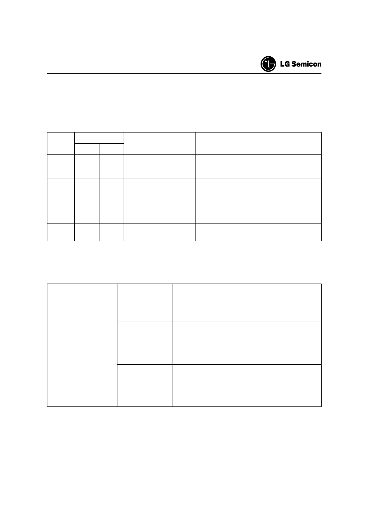
The serial port is full duplex and can operate in four modes (one synchronous mode, three asynchronous modes)
as illustrated in Table 6. The possible baud rates can be calculated using the formulas given in Table 7.
Table 6. USART Operating Modes
Mode
Baudrate Description
SM0 SM1
SCON
f
000
OSC
----------- -
12
1 0 1 Timer 1/2 overflow rate
f
210
OSC
----------- -
32
or
3 1 1 Timer 1/2 overflow rate
Table 7. Formulas for Calculating Baud rates
Baud Rate
derived from
Interface Mode Baudrate
0
Oscillator
2
f
OSC
----------- -
64
Serial data enters and exits through RxD.
TxD outputs the shift clock. 8-bit are transmitted/received (LSB first)
8-bit UART
10 bits are transmitted (through TxD) or
received (RxD)
9-bit UART
11 bits are transmitted (TxD) or received (RxD)
9-bit UART
Like mode 2 except the variable baud rate
f
OSC
----------- -
12
SMOD
2
----------------- -
×
f
64
OSC
SMOD
Timer 1 (16-bit timer)
1,3
2
----------------- -
32
()×
Timer 1 overflow
(8-bit timer with
8-bit auto reload)
Timer 2 1,3
1,3
SMOD
2
----------------- -
--------------------------------------------------------------------------------- -
32 65536 RC2H RC2L
32
×
[]×
f
f
–
[]×
OSC
OSC
–
()
,()
--------------------------------------------------
12 256 TH1
Dec. 1998 Ver 3.0 21
Page 26
GMS90 Series
INTERRUPT SYSTEM
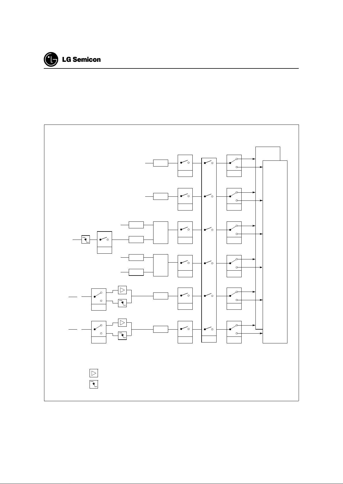
The GMS90 series provides 5 (4K bytes ROM version) or 6 (above 8K bytes ROM version) interrupt sources
with two priority levels. Figure 3 giv es a general overview of the interrupt sources and illustrates th e request and
control flags.
High
Priority
Timer 0 Overflow
TF0
TCON.5
ET0
IE.1
PT0
IP.1
Low
Priority
P1.1/
T2EX
P3.2/
INT0
P3.3/
INT1
Timer 1 Overflow
Timer 2 Overflow
EXEN2
T2CON.3
UART
IT0
TCON.0
IT1
TCON.2
TF2
T2CON.7
EXF2
T2CON.6
RI
SCON.0
TI
SCON.1
TF1
TCON.7
1
≥
1
≥
IE0
TCON.1
IE1
TCON.3
ET1
IE.3
ET2
IE.5
ES
IE.4
EX0
IE.0
EX1
IE.2
EA
IE.7
PT1
IP.3
PT2
IP.5
PS
IP.4
PX0
IP.0
PX1
IP.2
: Low level triggered
: Falling edge triggered
Figure 3. Interrupt Request Sources
22 Dec. 1998 Ver 3.0
Page 27
GMS90 Series
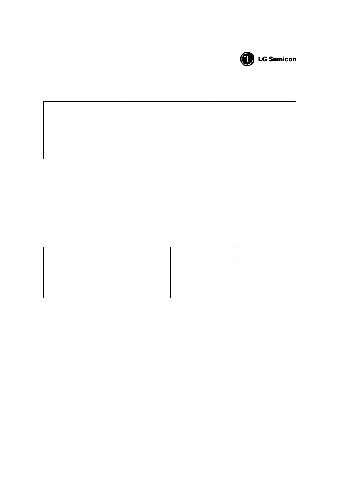
Table 8. Interrupt Sources and their Corresponding Interrupt Vectors
Source (Request Flags) Vectors Vector Address
RESET
IE0
TF0
IE1
TF1
RI + TI
TF2 + EXF2
RESET
External interrupt 0
Timer 0 interrupt
External interrupt 1
Timer 1 interrupt
Serial port interrupt
Timer 2 interrupt
0000H
0003H
000BH
0013H
001BH
0023H
002BH
A low-priority interrupt can itself be interrupted by a high -prior ity interrup t, b ut no t by ano ther lo w prio rity interrupt. A high-priority interrupt cannot be interrupted by any other interrupt source.
If two requests of different priority level are received simultaneously, the request of higher priority is serviced.
If requests of the same priority are received simultaneously, an internal polling sequence determines which request is serviced. Thus within each priority level there is a second priority structure determined by the polling
sequence as shown in Table 9.
Table 9. Interrupt Priority-Within-Level
Interrupt Source Priority
External Interrupt 0
Timer 0 Interrupt
External Interrupt 1
Timer 1 Interrupt
Serial Channel
Timer 2 Interrupt
IE0
TF0
IE1
TF1
RI + TI
TF2 + EXF2
High
↓
↓
↓
↓
Low
Dec. 1998 Ver 3.0 23
Page 28
GMS90 Series
Power Saving Modes
Two power down modes are available, the Idle Mode and Power Down Mode.
The bits PDE and IDLE of the register PCON select the Power Down mode or the Idle mode, respectively. If
the Power Down mode and the Idle mode are set at the same time, the P ower Down mode takes precedence.
Table 10 gives a general overvi ew of the power saving modes.
Table 10. Power Saving Modes Over view
Mode
Idle mode ORL PCON, #01H - Enabled interrupt
Power-Down mode ORL PCON, #02H Hardware Reset Oscillator is stopped, contents of on-
In the Power Down mode of operation, V
however, that V
is not reduced before the Power Down mode is invoked, and that VCC is restored to its normal
CC
Entering
Instruction
Example
Leaving by Remarks
CPU is gated off
- Hardware Reset
can be reduced to minimize power cons umption. It must be ensured,
CC
CPU status registers maintain their
data.
Peripherals are active
chip RAM and SFR’s are maintained
(leaving Power Down Mode means
redefinition of SFR contents).
operating level, before the Power Down mode is terminated. The reset signal that terminates the Power Down
mode also restarts the oscillator. The reset should not be activated befo re V
is restored to its normal operating
CC
level and must be held active long enough to allow the oscillator to restart and stabilize (similar to power-on
reset).
24 Dec. 1998 Ver 3.0
Page 29

GMS90 Series
ELECTRICAL CHARACTERISTICS
Absolute Maximum Ratings
Ambient temperature under bias (TA)......................................................................................-40 to + 85 °C
Storage temperature (T
Voltage on V
pins with respect to ground (VSS) .................................................................-0.5V to 6.5V
CC
Voltage on any pin with respect to ground (V
)...................................................................................................... -65 to + 150 °C
ST
) ..........................................................-0.5V to VCC + 0.5V
SS
Input current on any pin during overload condition............................. .... ...........................-15mA to +15mA
Absolute sum of all input currents during overload condition...........................................................|100mA|
Power dissipation....................................................................................................................................1.5W
Note: Stresses above those listed under "Absolu te Maximum Rating s" may cause perma nent damage of the device. This is a stress rating only and fu nctional opera tion of the device at these or any other conditions ab ove
those indicated in the operational sections of this specification is not implied. Exposure to absolute maximum rating conditions for lo nger peri ods may affe ct device rel iability. D uring ove rload cond itions ( VIN > VCC or VIN < VSS)
the Voltage on VCC pins with respect to ground (VSS) must not exceed the values defined by the absolute maximum ratings.
Dec. 1998 Ver 3.0 25
Page 30
DC Characteristics
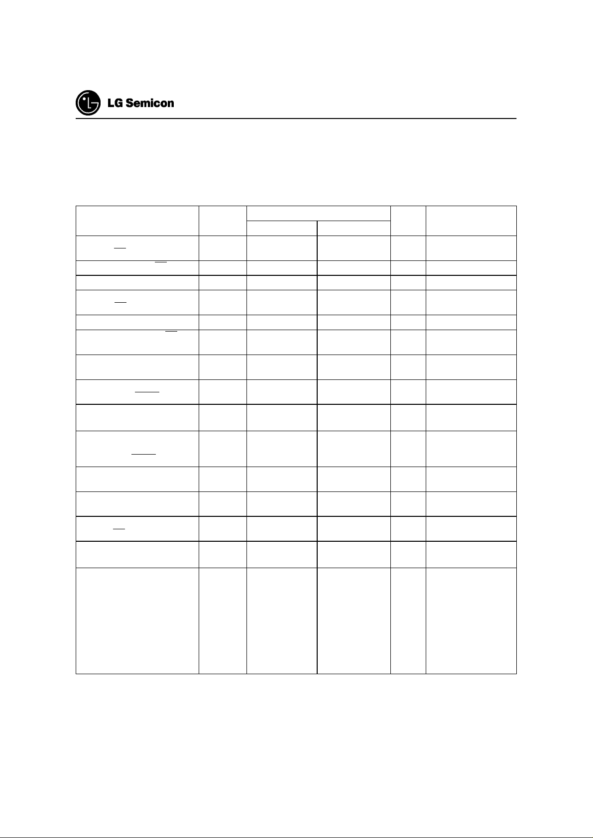
DC Characteristics for GMS90C31/32, GMS90C51/52/54/56/58
V
= 5V + 10%, -15%; VSS=0V; TA= 0°C to 70°C
CC
GMS90 Series
Parameter Symbol
Input low voltage
(except EA, RESET)
Input low voltage (EA)V
Input low voltage (RESET) V
Input high voltage (except
XTAL1, EA, RESET)
Input high voltage to XTAL1 V
Input high voltage to EA,
RESET
Output low voltage
(ports 1, 2, 3)
Output low voltage
(port 0, ALE, PSEN)
Output high voltage
(ports 1, 2, 3)
V
V
V
V
V
V
OL1
IL
IL1
IL2
IH
IH1
IH2
OL
OH
0.2VCC + 0.9 VCC + 0.5
Output high voltage
(port 0 in external bus
V
OH1
mode, ALE, PSEN)
Logic 0 input current
(ports 1, 2, 3)
Logical 1-to-0 transition cur-
rent (ports 1, 2, 3)
Input leakage current
(port 0, EA)
Pin capacitance
Power supply current:
Active mode, 12MHz
Idle mode, 12MHz
Active mode, 24 MHz
Idle mode, 24MHz
Active mode, 40 MHz
Idle mode, 40 MHz
Power Down Mode
3)
3)
3)
3)
3)
3)
3)
I
IL
I
TL
I
LI
C
IO
I
CC
I
CC
I
CC
I
CC
I
CC
I
CC
I
PD
Limit Values
Min. Max.
-0.5
-0.5
-0.5
0.2VCC - 0.1
0.2VCC - 0.3
0.2VCC + 0.1
Unit Test Conditions
VV-
VV-
0.7V
CC
0.6V
CC
-0.45V
-0.45V
2.4
0.9V
CC
2.4
0.9V
CC
-10 -50 µA
-65 -650 µA
- ±1 µA
-10pF
-
-
-
-
-
-
-
VCC + 0.5
VCC + 0.5
-V
-V
21
4.8
36.2
8.2
58.5
12.5
50
VV-
IOL= 1.6mA
IOL= 3.2mA
IOH= -80µA
IOH= -10µA
IOH= -800µA
IOH= -80µA
VIN= 0.45V
VIN= 2.0V
0.45 < VIN < V
fC= 1MHz
TA= 25°C
mA
VCC= 5V
mA
VCC= 5V
mA
VCC= 5V
mA
VCC= 5V
mA
VCC= 5V
mA
VCC= 5V
µ
A
VCC= 5V
1)
1)
2)
2)
CC
4)
5)
4)
5)
4)
5)
6)
26 Dec. 1998 Ver 3.0
Page 31

GMS90 Series
1) Capacitive loading on ports 0 and 2 may caus e spurious noise pulses to be superimposed on the VOL of ALE and port 3.
The noise is due to external bus capacitance discharging into the port 0 and port 2 pins when these pins make 1-to-0 transitions during bus operation. In the worst case (capacitive loading: > 50pF at 3.3V, > 100pF at 5V), the noise pulse on ALE
line may exceed 0.8V. In such cases it may be desirable to qualify ALE with a schmitt-trigger, or use an address latch with
a schmitt-trigger strobe input.
2) Capacitive loading on ports 0 and 2 may cause the V
tion when the address lines are stabilizing.
3) I
Max at other frequencies is given by:
CC
active mode: I
idle mode: I
where f
OSC
(active mode) is measured with:
4) I
CC
XTAL1 driven with t
EA
= Port0 = RESET = VCC; all other pins are disconnected. ICC would be slightly higher if a crystal oscillator is used (appr.
= 1.27 × f
CC
= 0.28 × f
CC
+ 5.73
OSC
+ 1.45 (except OTP devices)
OSC
is the oscillator frequency in MHz. ICC values are given in mA and measured at VCC = 5V .
, t
CLCH
= 5ns, VIL = VSS + 0.5V, VIH = VCC - 0.5V; XTAL2 = N.C.;
CHCL
1mA).
(Idle mode) is measured with all output pins disconnected and with all peripherals disabled;
5) I
CC
XTAL1 driven with t
RESET = EA
(Power Down Mode) is measured under following cond ition s:
6) I
PD
= Port0 = VCC; RESET = VSS; XTAL2 = N.C.; XTAL1 = VSS; all other pins are disconnected.
EA
= VSS; Port0 = VCC; all other pins are disconnected;
CLCH
, t
= 5ns, VIL = VSS + 0.5V, VIH = VCC - 0.5V; XTAL2 = N.C.;
CHCL
on ALE and PSEN to momentarily fall below the 0.9VCC specifica-
OH
Dec. 1998 Ver 3.0 27
Page 32
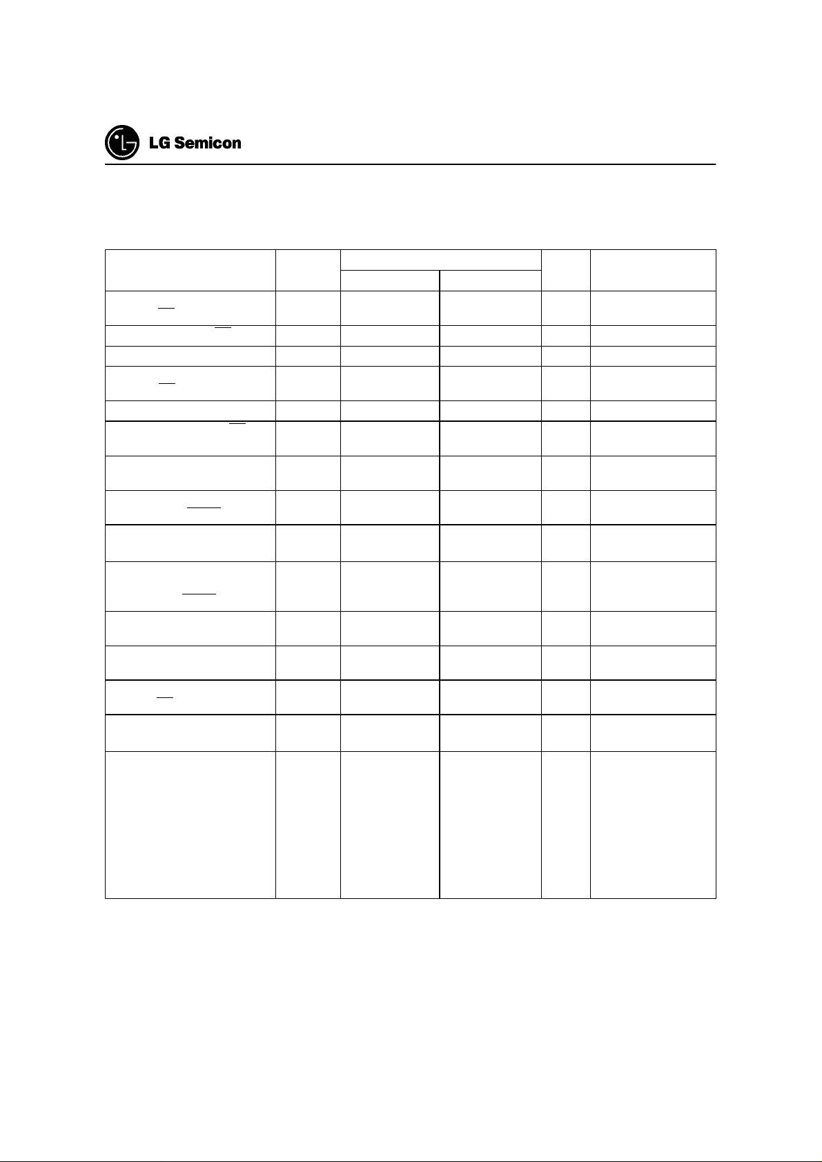
DC Characteristics for GMS97C51/52/54/56/58 (H)
V
= 5V + 10%, -15%; VSS=0V; TA= 0°C to 70°C
CC
GMS90 Series
Parameter Symbol
Input low voltage
(except EA, RESET)
Input low voltage (EA)V
Input low voltage (RESET) V
Input high voltage (except
XTAL1, EA, RESET)
Input high voltage to XTAL1 V
Input high voltage to EA,
RESET
Output low voltage
(ports 1, 2, 3)
Output low voltage
(port 0, ALE, PSEN)
Output high voltage
(ports 1, 2, 3)
V
V
V
V
V
V
OL1
IL
IL1
IL2
IH
IH1
IH2
OL
OH
0.2VCC + 0.9 VCC + 0.5
Output high voltage
(port 0 in external bus
V
OH1
mode, ALE, PSEN)
Logic 0 input current
(ports 1, 2, 3)
Logical 1-to-0 transition cur-
rent (ports 1, 2, 3)
Input leakage current
(port 0, EA)
Pin capacitance
Power supply current:
Active mode, 12MHz
Idle mode, 12MHz
Active mode, 24 MHz
Idle mode, 24MHz
Active mode, 33 MHz
Idle mode, 33 MHz
Power Down Mode
3)
3)
3)
3)
3)
3)
3)
I
IL
I
TL
I
LI
C
IO
I
CC
I
CC
I
CC
I
CC
I
CC
I
CC
I
PD
Limit Values
Min. Max.
-0.5
-0.5
-0.5
0.2VCC - 0.1
0.2VCC - 0.3
0.2VCC + 0.1
Unit Test Conditions
VV-
VV-
0.7V
CC
0.6V
CC
-0.45V
-0.45V
2.4
0.9V
CC
2.4
0.9V
CC
-10 -50 µA
-65 -650 µA
- ±1 µA
-10pF
-
-
-
-
-
-
-
VCC + 0.5
VCC + 0.5
-V
-V
21
4.8
36.2
8.2
45
10
50
VV-
IOL= 1.6mA
IOL= 3.2mA
IOH= -80µA
IOH= -10µA
IOH= -800µA
IOH= -80µA
VIN= 0.45V
VIN= 2.0V
0.45 < VIN < V
fC= 1MHz
TA= 25°C
mA
VCC= 5V
mA
VCC= 5V
mA
VCC= 5V
mA
VCC= 5V
mA
VCC= 5V
mA
VCC= 5V
µ
A
VCC= 5V
1)
1)
2)
2)
CC
4)
5)
4)
5)
4)
5)
6)
28 Dec. 1998 Ver 3.0
Page 33
GMS90 Series
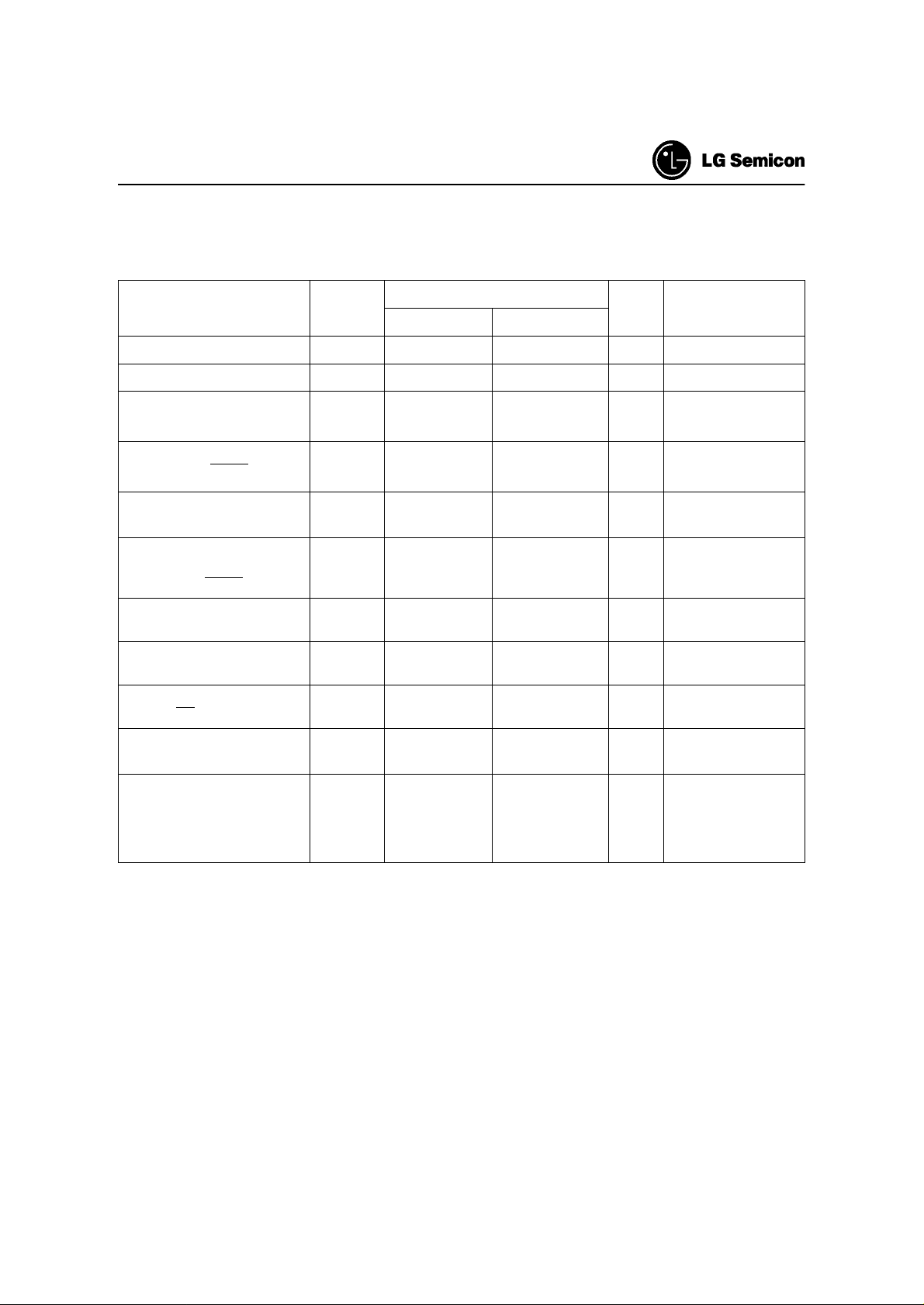
DC Characteristics for GMS90L31/32, GMS90L51/52/54/56/58
V
= 3.3V + 0.3V, -0.6V; VSS=0V; TA= 0°C to 70°C
CC
Parameter Symbol
Input low voltage V
Input high voltage V
Output low voltage
(ports 1, 2, 3)
Output low voltage
(port 0, ALE, PSEN)
Output high voltage
(ports 1, 2, 3)
V
V
V
Output high voltage
(port 0 in external bus
V
mode, ALE, PSEN)
Logic 0 input current
(ports 1, 2, 3)
Logical 1-to-0 transition cur-
rent (ports 1, 2, 3)
Input leakage current
(port 0, EA)
Pin capacitance
OL1
OH1
I
I
I
C
IL
IH
OL
OH
IL
TL
LI
IO
Limit Values
Unit Test Conditions
Min. Max.
-0.5 0.8 V -
2.0
-
-
2.0
0.9V
CC
2.0
0.9V
CC
-1 -50 µA
-25 -250 µA
- ±1 µA
-10pF
VCC + 0.5
0.45
0.30
0.45
0.30
V-
V
V
-V
-V
IOL= 1.6mA
IOL= 100µA
IOL= 3.2mA
IOL= 200µA
IOH= -20µA
IOH= -10µA
IOH= -800µA
IOH= -80µA
VIN= 0.45V
VIN= 2.0V
0.45 < VIN < V
fC= 1MHz
TA= 25°C
1)
1)
1)
1)
2)
2)
CC
Power supply current:
Active mode, 16 MHz
Idle mode, 16MHz
Power Down Mode
3)
3)
3)
I
CC
I
CC
I
PD
-
-
-
15
5
10
mA
mA
µA
V
CC
VCC= 2.6V
VCC=2~ 5.5V
= 3.6V
4)
5)
6)
Dec. 1998 Ver 3.0 29
Page 34
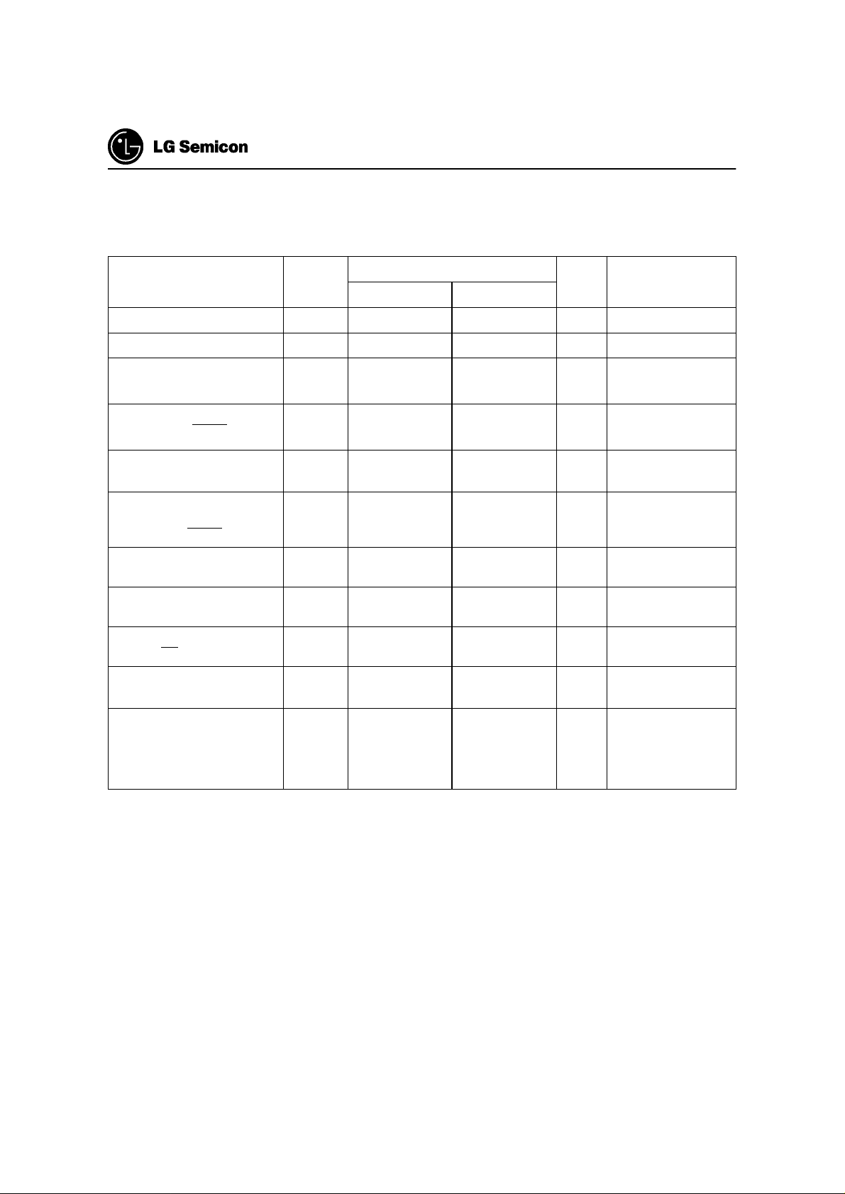
DC Characteristics for GMS97L51/52/54/56/58
V
= 3.3V + 0.3V, -0.6V; VSS=0V; TA= 0°C to 70°C
CC
GMS90 Series
Parameter Symbol
Input low voltage V
Input high voltage V
Output low voltage
(ports 1, 2, 3)
Output low voltage
(port 0, ALE, PSEN)
Output high voltage
(ports 1, 2, 3)
V
V
V
Output high voltage
(port 0 in external bus
V
mode, ALE, PSEN)
Logic 0 input current
(ports 1, 2, 3)
Logical 1-to-0 transition cur-
rent (ports 1, 2, 3)
Input leakage current
(port 0, EA)
Pin capacitance
OL
OL1
OH
OH1
I
IL
I
TL
I
LI
C
Limit Values
Unit Test Conditions
Min. max.
IL
IH
IO
-0.5 0.8 V -
2.0
-
-
2.0
0.9V
CC
2.0
0.9V
CC
-1 -50 µA
-25 -250 µA
- ±1 µA
-10pF
VCC + 0.5
0.45
0.30
0.45
0.30
V-
V
V
-V
-V
IOL= 1.6mA
IOL= 100µA
IOL= 3.2mA
IOL= 200µA
IOH= -20µA
IOH= -10µA
IOH= -800µA
IOH= -80µA
VIN= 0.45V
VIN= 2.0V
0.45 < VIN < V
fC= 1MHz
TA= 25°C
1)
1)
1)
1)
2)
2)
CC
Power supply current:
Active mode, 12MHz
Idle mode, 12MHz
Power Down Mode
3)
3)
3)
I
CC
I
CC
I
PD
-
-
-
15
10
mA
V
CC
5
mA
µA
VCC= 2.6V
VCC=2~ 5.5V
= 3.6V
4)
5)
6)
30 Dec. 1998 Ver 3.0
Page 35
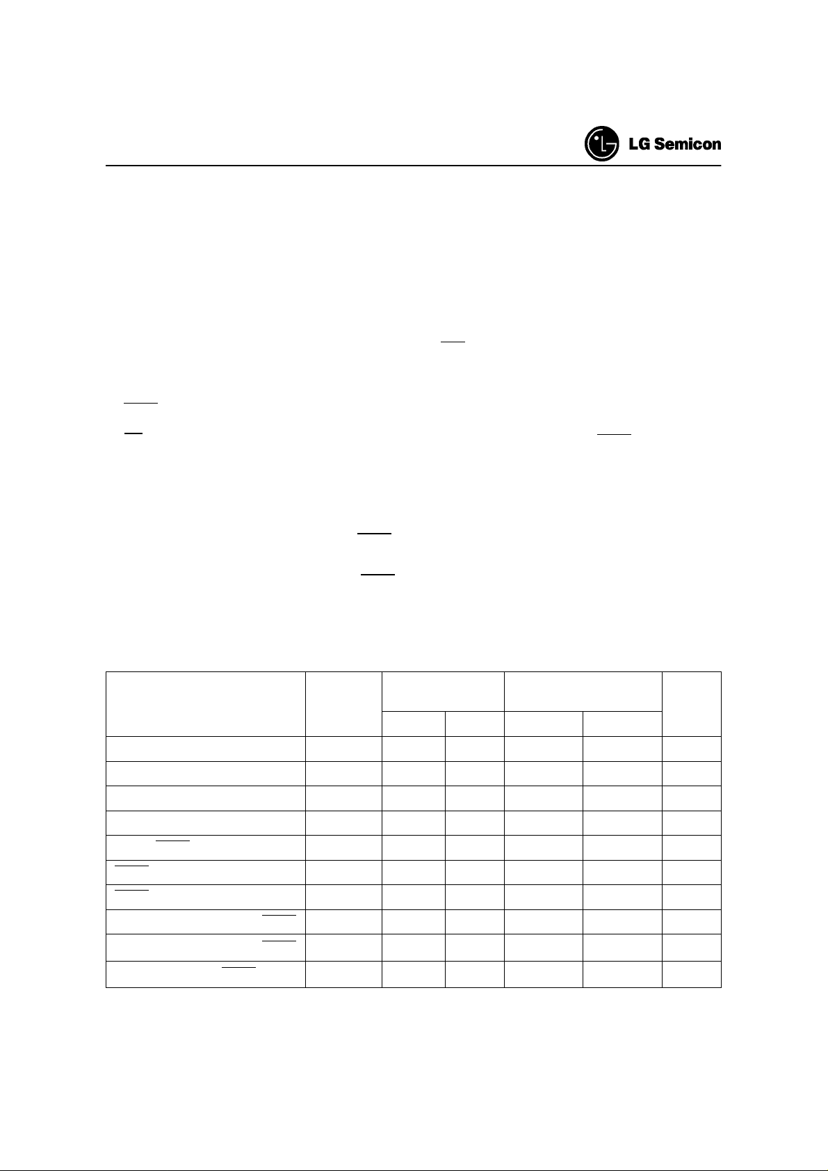
GMS90 Series
AC Characteristics
Explanation of the AC Symbols
Each timing symbol has 5 characters. Th e first c haracter is alwa ys a ‘t’ (stand for time). Th e ot her ch arac ters,
depending on their position s , sta n d for th e na m e of a sign al or the logical status of that sign al. The following is
a list of all the characters and what they stand for.
A: Address
C: Clock
D: Input Data
H: Logic level HIGH
I: Instruction (program memory contents)
L: Logic level LOW, or ALE
P: PSEN
Q: Output Data
R: RD signal
AC Characteristics for GMS90 series (12MHz version)
T: Time
V: Valid
W: WR signal
X: No longer a valid logic level
Z: Float
For example,
t
= Time from Address Valid to ALE Low
AVLL
t
= Time from ALE Low to PSEN Low
LLPL
VCC= 5V :
VCC= 5V + 10%, − 15%; VSS= 0V; TA= 0°C to 70°C
(CL for port 0. ALE and PSEN outputs = 100pF; CL for all other outputs = 80pF)
VCC= 3.3V :
VCC= 3.3V + 0.3V, − 0.6V; VSS= 0V; TA= 0°C to 70°C
(CL for port 0. ALE and PSEN outputs = 50pF; CL for all other outputs = 50pF)
Variable clock :
Vcc = 5V : 1/t
Vcc = 3.3V : 1/t
= 3.5 MHz to 12 MHz
CLCL
= 1 MHz to 12 MHz
CLCL
External Program Memory Characteristics
Parameter Symbol
ALE pulse width
Address setup to ALE
Address hold after ALE
ALE low to valid instruction in
ALE to PSEN
PSEN pulse width
PSEN to valid instruction in
Input instruction hold after PSEN
Input instruction float after PSEN
Address valid after PSEN
t
LHLL
t
AVLL
t
LLAX
t
LLIV
t
LLPL
t
PLPH
t
PLIV
t
PXIX
t
PXIZ
t
PXAV
†
†
12 MHz Oscillator
Variable Oscillator
1/t
= 3.5 to 12MHz
CLCL
Unit
Min. Max. Min. Max.
127 - 2t
43 - t
30 - t
-233 -4t
58 - t
215 - 3t
-150 -3t
-40 -
CLCL
-40 - ns
CLCL
-53 -
CLCL
-100 ns
CLCL
-25 -
CLCL
-35 - ns
CLCL
-100
CLCL
ns
ns
ns
ns
0- 0 - ns
-63 -t
75 - t
-8 - ns
CLCL
CLCL
-20
ns
Dec. 1998 Ver 3.0 31
Page 36
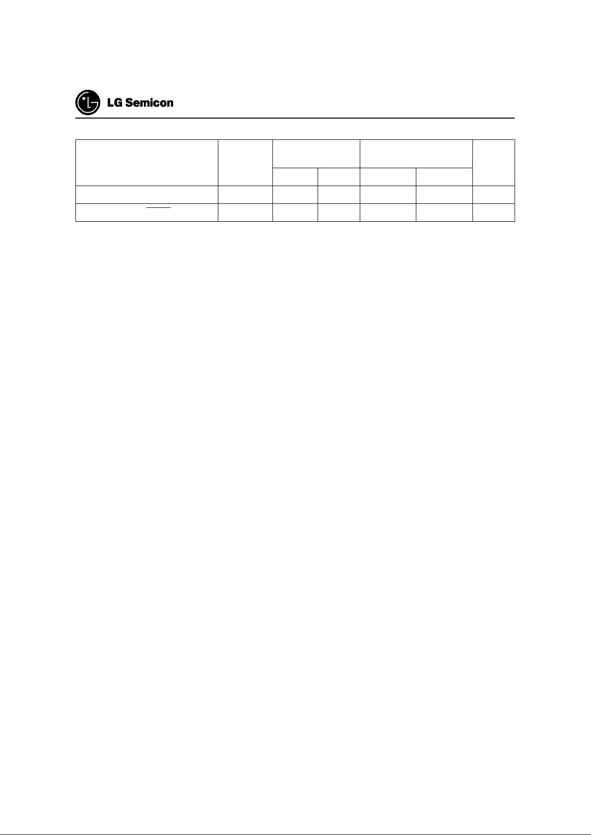
GMS90 Series
Parameter Symbol
12 MHz Oscillator
Variable Oscillator
1/t
= 3.5 to 12MHz
CLCL
Unit
Min. Max. Min. Max.
Address to valid instruction in
Address float to PSEN
†
Interfacing the GMS90 series to devices with float times up to 75 ns is permissible. This limited bus contention will not cause
any damage to port 0 Drivers.
t
AVIV
t
AZPL
-302 -5t
CLCL
-115
ns
0- 0 - ns
32 Dec. 1998 Ver 3.0
Page 37
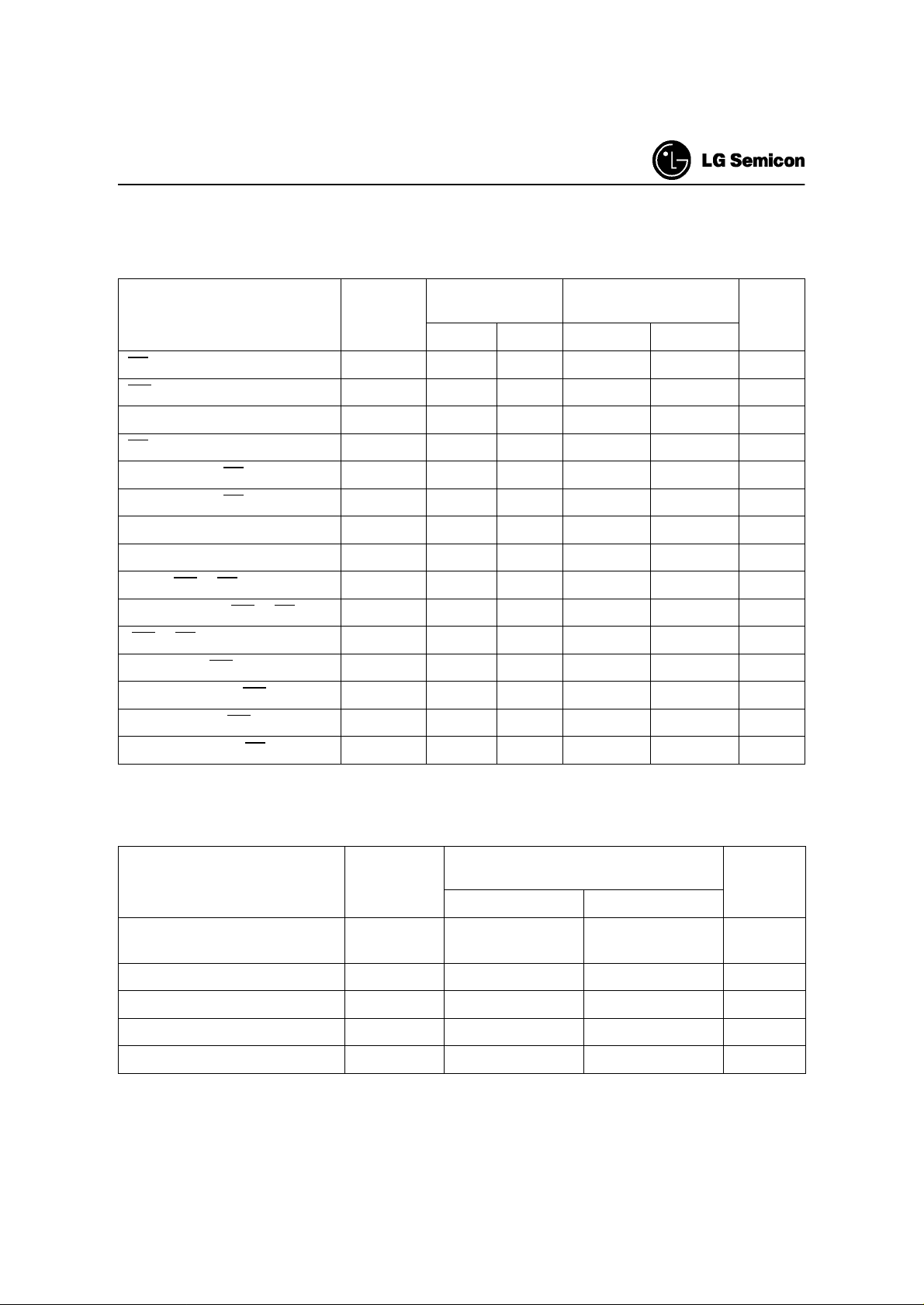
GMS90 Series
AC Characteristics for GMS90 series (12MHz)
External Data Memory Characteristics
Parameter Symbol
RD pulse width
WR pulse width
Address hold after ALE
RD to valid data in
Data hold after RD
Data float after RD
ALE to valid data in
Address to valid data in
ALE to WR or RD
Address valid to WR or RD
WR or RD high to ALE high
Data valid to WR transition
Data setup before WR
Data hold after WR
Address float after RD
t
RLRH
t
WLWH
t
LLAX2
t
RLDV
t
RHDX
t
RHDZ
t
LLDV
t
AVDV
t
LLWL
t
AVWL
t
WHLH
t
QVWX
t
QVWH
t
WHQX
t
RLAZ
12 MHz Oscillator
Variable Oscillator
1/t
= 3.5 to 12MHz
CLCL
Unit
Min. Max. Min. Max.
400 - 6t
400 - 6t
53 - t
-252 -5t
0- 0 -
-97 -2t
-517 -8t
-585 -9t
200 300 3t
203 - 4t
43 123 t
33 - t
433 - 7t
33 - t
-100 -
CLCL
-100 - ns
CLCL
-30 -
CLCL
-165 ns
CLCL
-70 ns
CLCL
-150
CLCL
-165 ns
CLCL
-50 3t
CLCL
-130 - ns
CLCL
-40 t
CLCL
-50 - ns
CLCL
-150 - ns
CLCL
-50 -
CLCL
CLCL
CLCL
+50
+40
ns
ns
ns
ns
ns
ns
ns
-0 - 0 ns
Advance Information (12MHz)
External Clock Drive
Variable Oscillator
Parameter Symbol
(Freq. = 3.5 to 12MHz)
Unit
Min. Max.
Oscillator period (VCC=5V)
Oscillator period (VCC=3.3V)
High time
Low time
Rise time
Fall time
t
CLCL
t
CLCL
t
CHCX
t
CLCX
t
CLCH
t
CHCL
83.3
83.3
20 t
20 t
CLCL
CLCL
285.7
1
- t
- t
CLCX
CHCX
ns
ns
ns
-20ns
-20
ns
Dec. 1998 Ver 3.0 33
Page 38
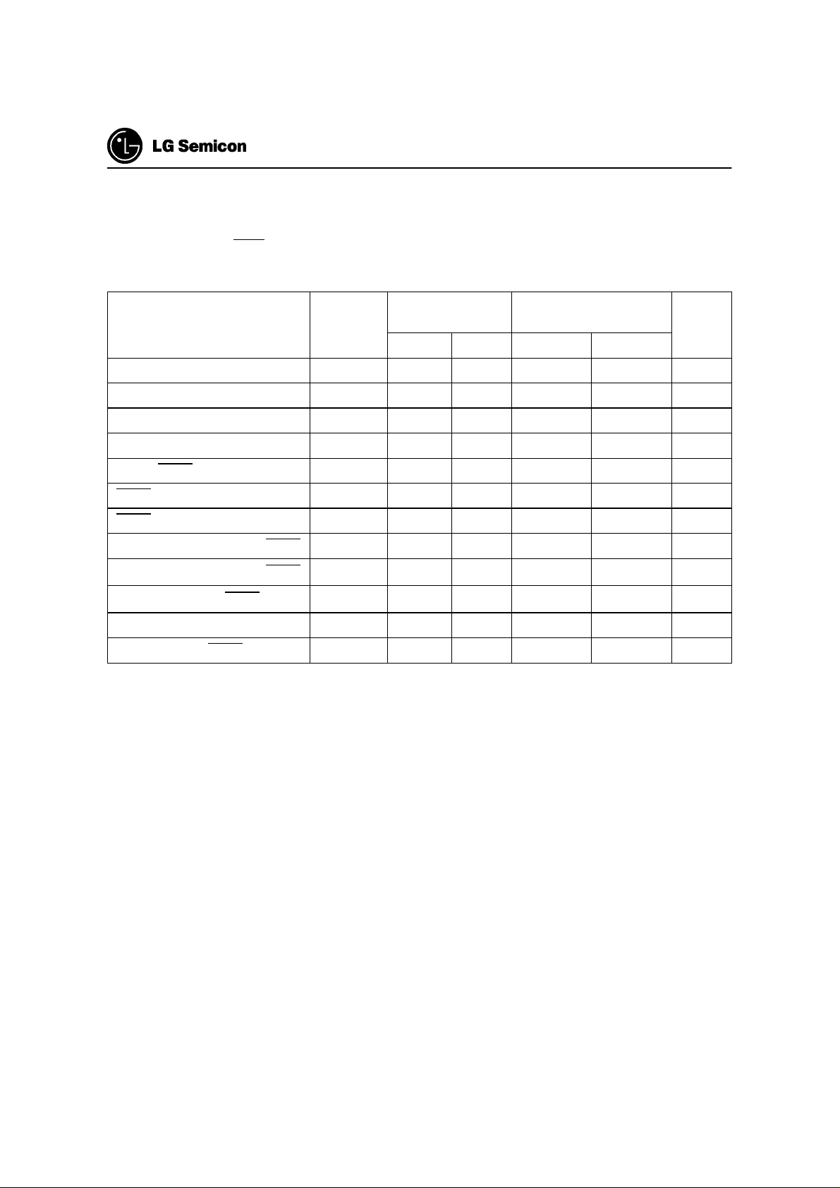
AC Characteristics for GMS90 series (16MHz version)
V
= 3.3V + 0.3V, −0.6V; VSS= 0V; TA= 0°C to 70°C
CC
(CL for port 0. ALE and PSEN outputs = 50pF; CL for all other outputs = 50pF)
External Program Memory Characteristics
GMS90 Series
Parameter Symbol
16 MHz Oscillator
Variable Oscillator
1/t
= 3.5 to 16MHz
CLCL
Unit
Min. Max. Min. Max.
ALE pulse width
Address setup to ALE
Address hold after ALE
ALE low to valid instruction in
ALE to PSEN
PSEN pulse width
PSEN to valid instruction in
Input instruction hold after PSEN
Input instruction float after PSEN
Address valid after PSEN
Address to valid instruction in
Address float to PSEN
†
Interfacing the GMS90 series to devices with float times up to 35 ns is permissible. This limited bus contention will not cause
any damage to port 0 Drivers.
t
LHLL
t
AVLL
t
LLAX
t
LLIV
t
LLPL
t
PLPH
t
PLIV
t
PXIX
t
PXIZ
t
PXAV
t
AVIV
t
AZPL
†
†
85 - 2t
23 - t
23 - t
-150 -4t
38 - t
153 - 3t
-88 -3t
-40 -
CLCL
-40 - ns
CLCL
-40 -
CLCL
-100 ns
CLCL
-25 -
CLCL
-35 - ns
CLCL
-100
CLCL
ns
ns
ns
ns
0- 0 - ns
-43 -t
55 - t
-8 - ns
CLCL
-198 -5t
CLCL
CLCL
-20
-115
ns
ns
0- 0 - ns
34 Dec. 1998 Ver 3.0
Page 39
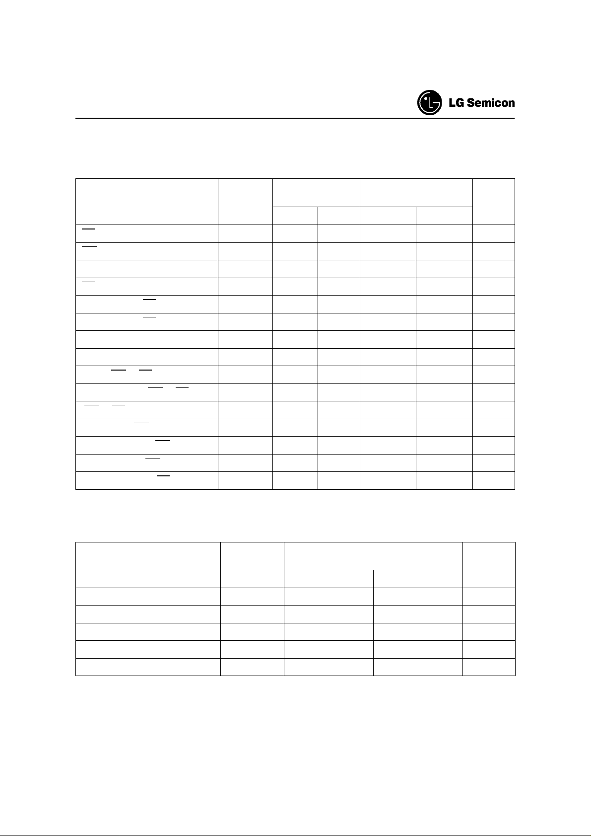
GMS90 Series
AC Characteristics for GMS90 series (16MHz)
External Data Memory Characteristics
Parameter Symbol
RD pulse width
WR pulse width
Address hold after ALE
RD to valid data in
Data hold after RD
Data float after RD
ALE to valid data in
Address to valid data in
ALE to WR or RD
Address valid to WR or RD
WR or RD high to ALE high
Data valid to WR transition
Data setup before WR
Data hold after WR
Address float after RD
t
RLRH
t
WLWH
t
LLAX2
t
RLDV
t
RHDX
t
RHDZ
t
LLDV
t
AVDV
t
LLWL
t
AVWL
t
WHLH
t
QVWX
t
QVWH
t
WHQX
t
RLAZ
16 MHz Oscillator
Variable Oscillator
1/t
= 3.5 to 16MHz
CLCL
Unit
Min. Max. Min. Max.
275 - 6t
275 - 6t
23 - t
-183 -5t
0- 0 -
-75 -2t
-350 -8t
-398 -9t
138 238 3t
120 - 4t
28 97 t
13 - t
288 - 7t
23 - t
-100 -
CLCL
-100 - ns
CLCL
-40 -
CLCL
-130 ns
CLCL
-50 ns
CLCL
-150
CLCL
-165 ns
CLCL
−50 3t
CLCL
-130 - ns
CLCL
−35 t
CLCL
−
50 - ns
CLCL
-150 - ns
CLCL
−40 -
CLCL
CLCL
CLCL
+50
+35
ns
ns
ns
ns
ns
ns
ns
-0 - 0 ns
Advance Information (16MHz)
External Clock Drive
Variable Oscillator
Parameter Symbol
(Freq. = 3.5 to 16MHz)
Unit
Min. Max.
Oscillator period
High time
Low time
Rise time
Fall time
t
CLCL
t
CHCX
t
CLCX
t
CLCH
t
CHCL
62.5 285.7
17 t
17 t
CLCL
CLCL
- t
- t
CLCX
CHCX
ns
ns
ns
-17ns
-17
ns
Dec. 1998 Ver 3.0 35
Page 40
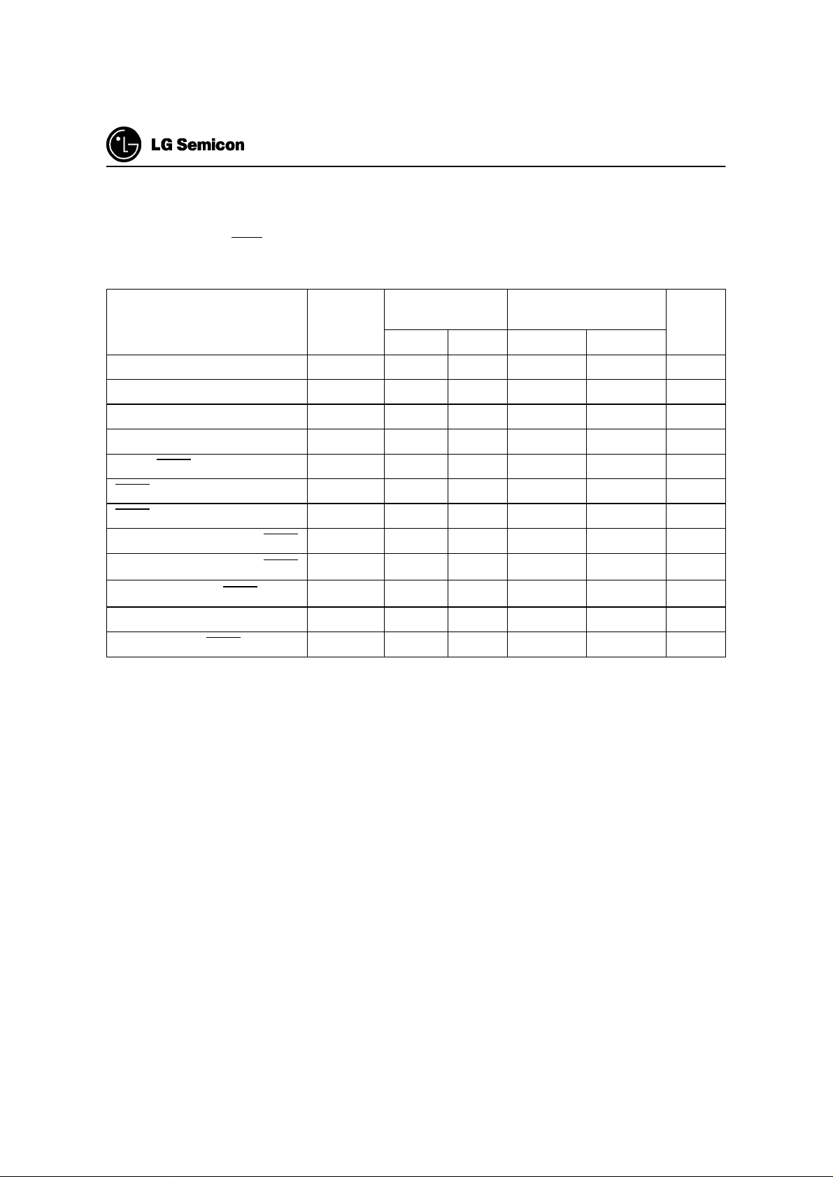
AC Characteristics for GMS90 series (24MHz version)
V
= 5V + 10%, −15%; VSS= 0V; TA= 0°C to 70°C
CC
(CL for port 0. ALE and PSEN outputs = 100pF; CL for all other outputs = 80pF)
External Program Memory Characteristics
GMS90 Series
Parameter Symbol
24 MHz Oscillator
Variable Oscillator
1/t
= 3.5 to 24MHz
CLCL
Unit
Min. Max. Min. Max.
ALE pulse width
Address setup to ALE
Address hold after ALE
ALE low to valid instruction in
ALE to PSEN
PSEN pulse width
PSEN to valid instruction in
Input instruction hold after PSEN
Input instruction float after PSEN
Address valid after PSEN
Address to valid instruction in
Address float to PSEN
†
Interfacing the GMS90 series to devices with float times up to 35 ns is permissible. This limited bus contention will not cause
any damage to port 0 Drivers.
t
LHLL
t
AVLL
t
LLAX
t
LLIV
t
LLPL
t
PLPH
t
PLIV
t
PXIX
t
PXIZ
t
PXAV
t
AVIV
t
AZPL
†
†
43 - 2t
17 - t
17 - t
-80 -4t
22 - t
95 - 3t
-60 -3t
-40 -
CLCL
-25 - ns
CLCL
-25 -
CLCL
-87 ns
CLCL
-20 -
CLCL
-30 - ns
CLCL
-65
CLCL
ns
ns
ns
ns
0- 0 - ns
-32 -t
37 - t
-5 - ns
CLCL
-148 -5t
CLCL
CLCL
-10
-60
ns
ns
0- 0 - ns
36 Dec. 1998 Ver 3.0
Page 41
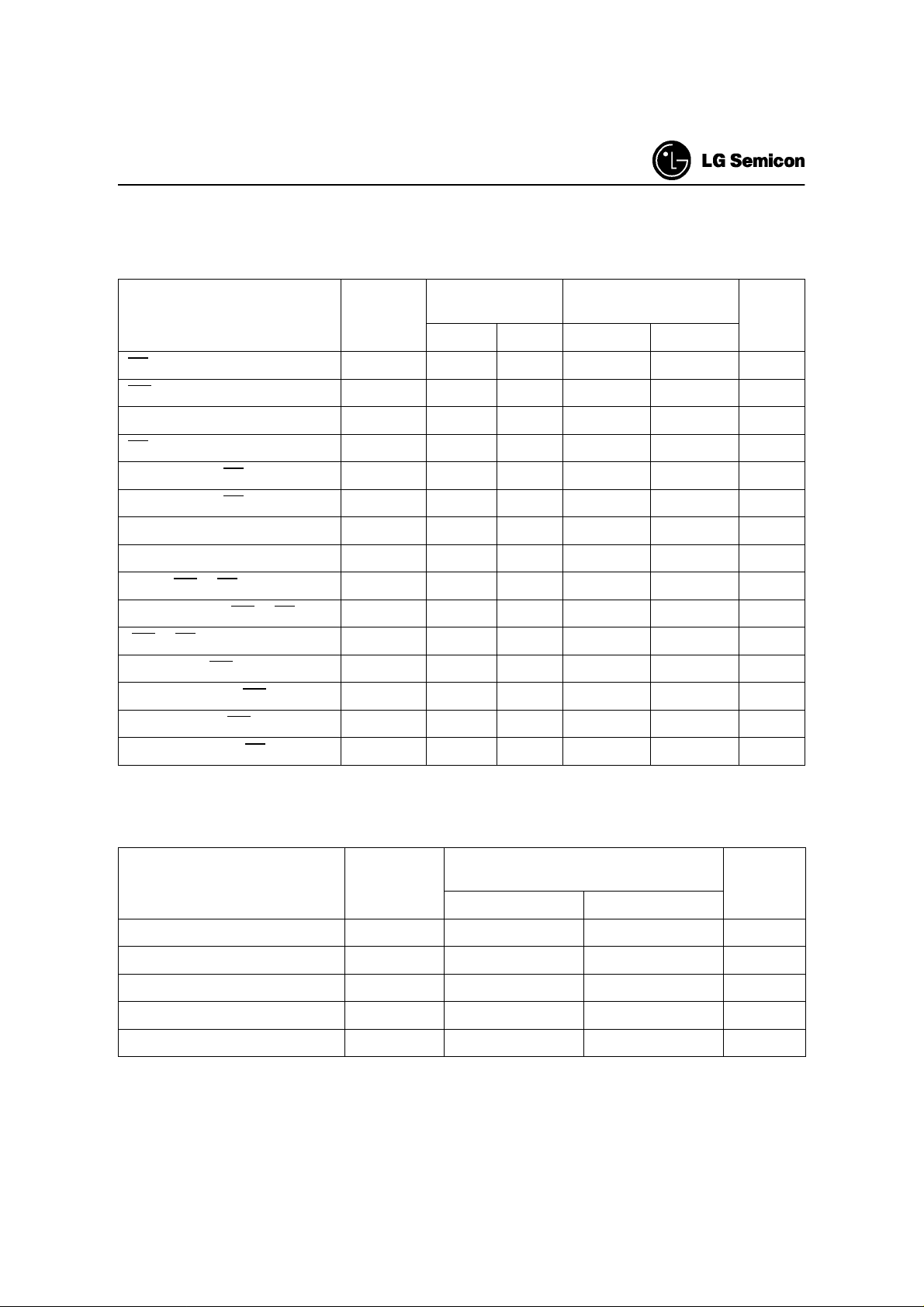
GMS90 Series
AC Characteristics for GMS90 series (24MHz)
External Data Memory Characteristics
Parameter Symbol
RD pulse width
WR pulse width
Address hold after ALE
RD to valid data in
Data hold after RD
Data float after RD
ALE to valid data in
Address to valid data in
ALE to WR or RD
Address valid to WR or RD
WR or RD high to ALE high
Data valid to WR transition
Data setup before WR
Data hold after WR
Address float after RD
t
RLRH
t
WLWH
t
LLAX2
t
RLDV
t
RHDX
t
RHDZ
t
LLDV
t
AVDV
t
LLWL
t
AVWL
t
WHLH
t
QVWX
t
QVWH
t
WHQX
t
RLAZ
24 MHz Oscillator
Variable Oscillator
1/t
= 3.5 to 24MHz
CLCL
Unit
Min. Max. Min. Max.
180 - 6t
180 - 6t
15 - t
-118 -5t
0- 0 -
-63 -2t
-200 -8t
-220 -9t
75 175 3t
67 - 4t
17 67 t
5-t
170 - 7t
15 - t
-70 -
CLCL
-70 - ns
CLCL
-27 -
CLCL
-90 ns
CLCL
-20 ns
CLCL
-133
CLCL
-155 ns
CLCL
-50 3t
CLCL
-97 - ns
CLCL
-25 t
CLCL
-37 - ns
CLCL
-122 - ns
CLCL
-27 -
CLCL
CLCL
CLCL
+50
+25
ns
ns
ns
ns
ns
ns
ns
-0 - 0 ns
Advance Information (24MHz)
External Clock Drive
Variable Oscillator
Parameter Symbol
(Freq. = 3.5 to 24MHz)
Unit
Min. Max.
Oscillator period
High time
Low time
Rise time
Fall time
t
CLCL
t
CHCX
t
CLCX
t
CLCH
t
CHCL
41.7 285.7
12 t
12 t
CLCL
CLCL
- t
- t
CLCX
CHCX
ns
ns
ns
-12ns
-12
ns
Dec. 1998 Ver 3.0 37
Page 42
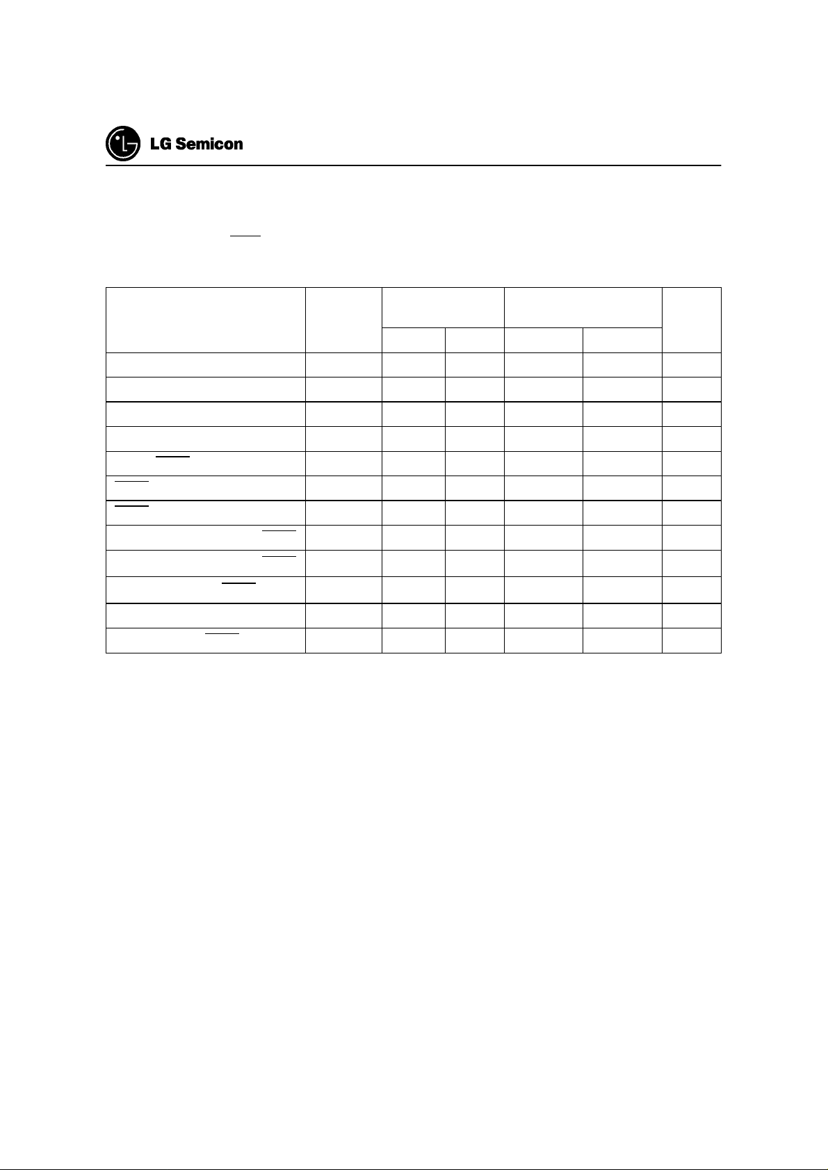
AC Characteristics for GMS90 series (33MHz version)
V
= 5V + 10%, −15%; VSS= 0V; TA= 0°C to 70°C
CC
(CL for port 0. ALE and PSEN outputs = 100pF; CL for all other outputs = 80pF)
External Program Memory Characteristics
GMS90 Series
Parameter Symbol
33 MHz Oscillator
Variable Oscillator
1/t
= 3.5 to 33MHz
CLCL
Unit
Min. Max. Min. Max.
ALE pulse width
Address setup to ALE
Address hold after ALE
ALE low to valid instruction in
ALE to PSEN
PSEN pulse width
PSEN to valid instruction in
Input instruction hold after PSEN
Input instruction float after PSEN
Address valid after PSEN
Address to valid instruction in
Address float to PSEN
†
Interfacing the GMS90 series to devices with float times up to 35 ns is permissible. This limited bus contention will not cause
any damage to port 0 Drivers.
t
LHLL
t
AVLL
t
LLAX
t
LLIV
t
LLPL
t
PLPH
t
PLIV
t
PXIX
t
PXIZ
t
PXAV
t
AVIV
t
AZPL
†
†
40 - 2t
10 - t
10 - t
-56 -4t
15 - t
80 - 3t
-35 -3t
-20 -
CLCL
-20 - ns
CLCL
-20 -
CLCL
-65 ns
CLCL
-15 -
CLCL
-20 - ns
CLCL
-55
CLCL
ns
ns
ns
ns
0- 0 - ns
-20 -t
25 - t
-5 - ns
CLCL
-91 -5t
CLCL
CLCL
-10
-60
ns
ns
0- 0 - ns
38 Dec. 1998 Ver 3.0
Page 43
GMS90 Series
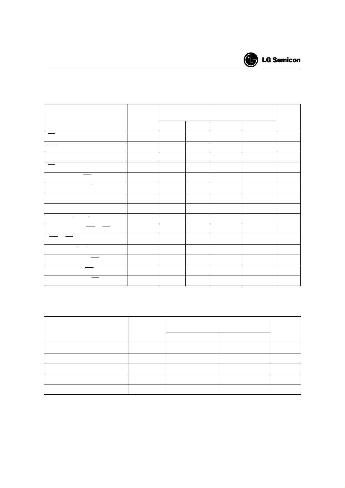
AC Characteristics for GMS90 series (33MHz)
External Data Memory Characteristics
Parameter Symbol
RD pulse width
WR pulse width
Address hold after ALE
RD to valid data in
Data hold after RD
Data float after RD
ALE to valid data in
Address to valid data in
ALE to WR or RD
Address valid to WR or RD
WR or RD high to ALE high
Data valid to WR transition
Data setup before WR
Data hold after WR
Address float after RD
t
RLRH
t
WLWH
t
LLAX2
t
RLDV
t
RHDX
t
RHDZ
t
LLDV
t
AVDV
t
LLWL
t
AVWL
t
WHLH
t
QVWX
t
QVWH
t
WHQX
t
RLAZ
33 MHz Oscillator
Variable Oscillator
1/t
= 3.5 to 33MHz
CLCL
Unit
Min. Max. Min. Max.
132 - 6t
132 - 6t
10 - t
-81 -5t
0- 0 -
-46 -2t
-153 -8t
-183 -9t
71 111 3t
66 - 4t
10 40 t
5-t
142 - 7t
10 - t
-50 -
CLCL
-50 - ns
CLCL
-20 -
CLCL
-70 ns
CLCL
-15 ns
CLCL
-90
CLCL
-90 ns
CLCL
-20 3t
CLCL
-55 - ns
CLCL
-20 t
CLCL
-25 - ns
CLCL
-70 - ns
CLCL
-20 -
CLCL
CLCL
CLCL
+20
+20
ns
ns
ns
ns
ns
ns
ns
-0 - 0 ns
Advance Information (33MHz)
External Clock Drive
Variable Oscillator
Parameter Symbol
(Freq. = 3.5 to 24MHz)
Unit
Min. Max.
Oscillator period
High time
Low time
Rise time
Fall time
t
CLCL
t
CHCX
t
CLCX
t
CLCH
t
CHCL
30.3 285.7
11.5 t
11.5 t
CLCL
CLCL
- t
- t
CLCX
CHCX
ns
ns
ns
-5ns
-5
ns
Dec. 1998 Ver 3.0 39
Page 44
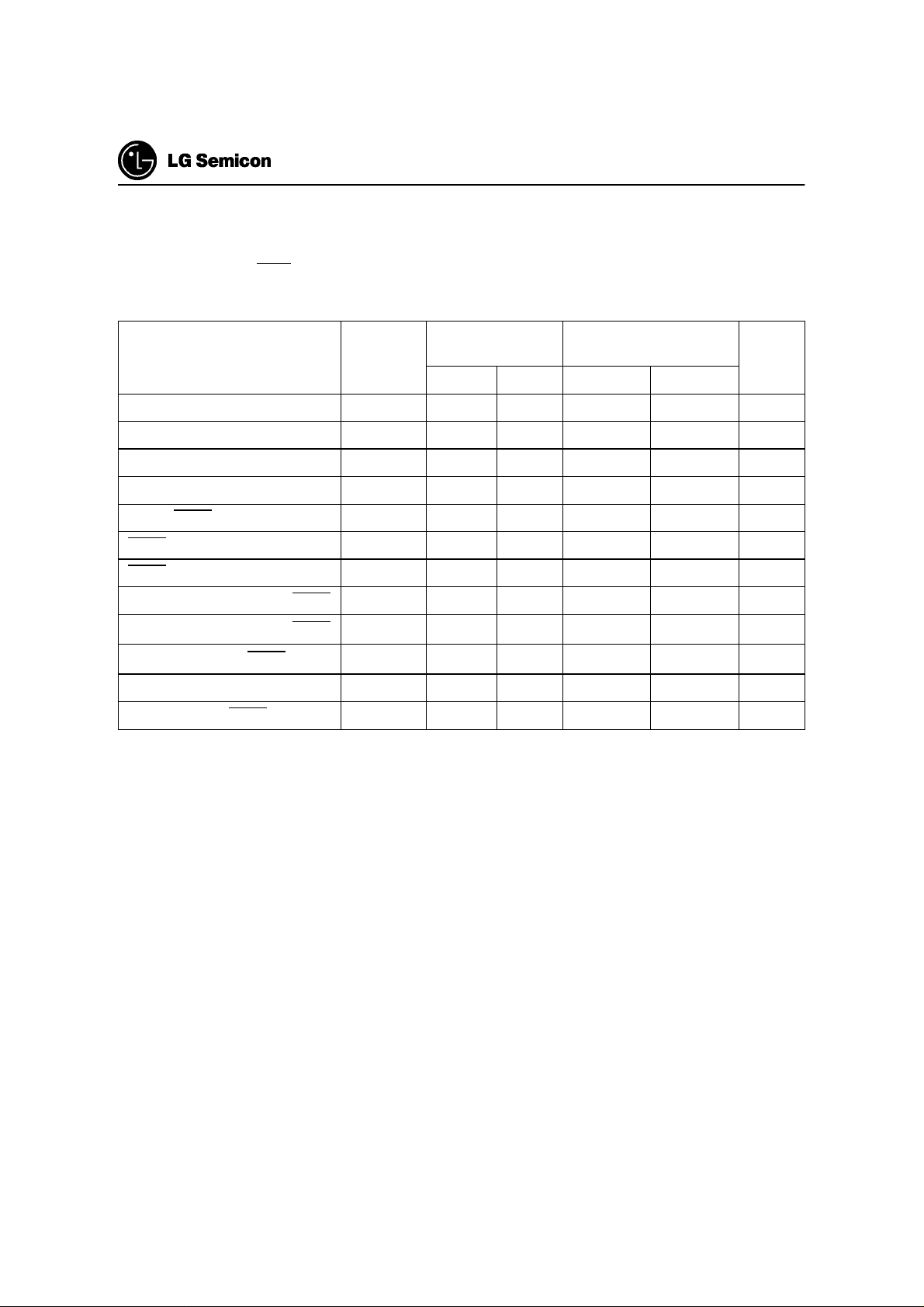
AC Characteristics for GMS90 series (40MHz version)
V
= 5V + 10%, − 15%; VSS= 0V; TA= 0°C to 70°C
CC
(CL for port 0. ALE and PSEN outputs = 100pF; CL for all other outputs = 80pF)
External Program Memory Characteristics
GMS90 Series
Parameter Symbol
40 MHz Oscillator
Variable Oscillator
1/t
= 3.5 to 40MHz
CLCL
Unit
Min. Max. Min. Max.
ALE pulse width
Address setup to ALE
Address hold after ALE
ALE low to valid instruction in
ALE to PSEN
PSEN
pulse width
PSEN
to valid instruction in
Input instruction hold after PSEN
Input instruction float after PSEN
Address valid after PSEN
Address to valid instruction in
Address float to PSEN
†
Interfacing the GMS90 series to devices with float times up to 20 ns is permissible. This limited bus contention will not cause
any damage to port 0 Drivers.
t
LHLL
t
AVLL
t
LLAX
t
LLIV
t
LLPL
t
PLPH
t
PLIV
t
PXIX
t
PXIZ
t
PXAV
t
AVIV
t
AZPL
†
†
35 - 2t
10 - t
10 - t
-55 -4t
10 - t
60 - 3t
-25 -3t
0- 0 - ns
-15 -t
20 - t
-65 -5t
5- 5 - ns
−
15 -
CLCL
−15 - ns
CLCL
−15 -
CLCL
−45 ns
CLCL
−15 -
CLCL
−15 - ns
CLCL
−50
CLCL
−10
CLCL
−5- ns
CLCL
−60
CLCL
ns
ns
ns
ns
ns
ns
40 Dec. 1998 Ver 3.0
Page 45
GMS90 Series
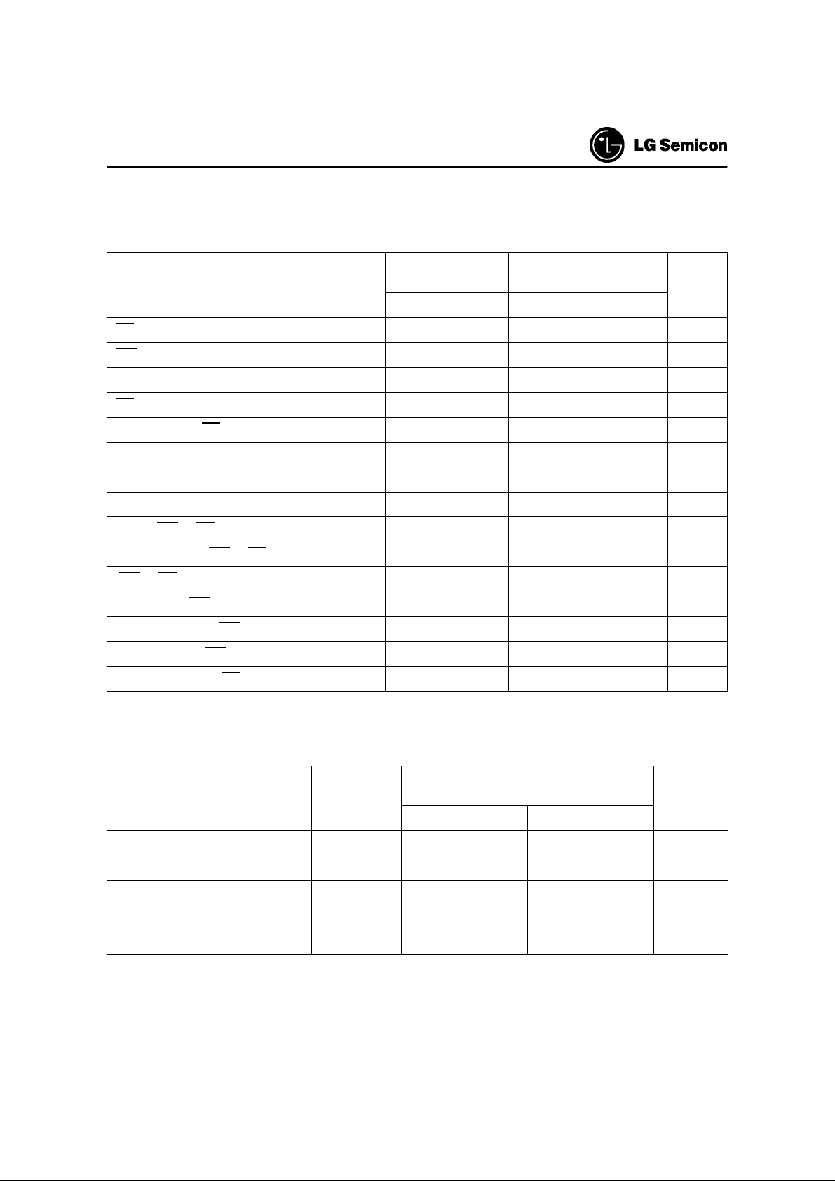
AC Characteristics for GMS90 series (40MHz)
External Data Memory Characteristics
Parameter Symbol
RD pulse width
WR pulse width
Address hold after ALE
RD to valid data in
Data hold after RD
Data float after RD
ALE to valid data in
Address to valid data in
ALE to WR or RD
Address valid to WR or RD
WR or RD high to ALE high
Data valid to WR transition
Data setup before WR
Data hold after WR
Address float after RD
t
RLRH
t
WLWH
t
LLAX2
t
RLDV
t
RHDX
t
RHDZ
t
LLDV
t
AVDV
t
LLWL
t
AVWL
t
WHLH
t
QVWX
t
QVWH
t
WHQX
t
RLAZ
at 40 MHz Clock
Variable Clock
1/t
= 3.5 to 40MHz
CLCL
Unit
Min. Max. Min. Max.
120 - 6t
120 - 6t
10 - t
-75 -5t
0- 0 -
-38 -2t
-150 -8t
-150 -9t
60 90 3t
70 - 4t
10 40 t
5-t
125 - 7t
5-t
-30 -
CLCL
-30 - ns
CLCL
-15 -
CLCL
-50 ns
CLCL
-12 ns
CLCL
-50
CLCL
-75 ns
CLCL
-15 3t
CLCL
-30 - ns
CLCL
-15 t
CLCL
-20 - ns
CLCL
-50 - ns
CLCL
-20 -
CLCL
CLCL
CLCL
+15
+15
ns
ns
ns
ns
ns
ns
ns
-0 - 0 ns
Advance Information (40MHz)
External Clock Drive
Variable Oscillator
Parameter Symbol
(Freq. = 3.5 to 40MHz)
Unit
Min. Max.
Oscillator period
High time
Low time
Rise time
Fall time
t
CLCL
t
CHCX
t
CLCX
t
CLCH
t
CHCL
25 285.7
10 t
10 t
CLCL
CLCL
- t
- t
CLCX
CHCX
ns
ns
ns
-10ns
-10
ns
Dec. 1998 Ver 3.0 41
Page 46
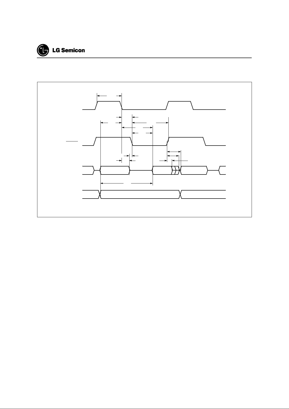
ALE
PSEN
PORT 0
t
LHLL
t
AVLL
t
LLAX
A0-A7
t
AZPL
t
AVIV
t
LLIV
t
t
PLIV
LLPL
t
PLPH
INSTR.
IN
t
PXAV
t
PXIZ
t
PXIX
A0-A7
GMS90 Series
PORT 2
A8-A15
Figure 4. External Program Memory Read Cycle
A8-A15
42 Dec. 1998 Ver 3.0
Page 47
GMS90 Series
ALE
t
LHLL
PSEN
t
LLWL
RD
t
AVLL
t
LLAX2
PORT 0
PORT 2
A0-A7 from
RI or DPL
t
AVWL
t
P2.0-P2.7 or A8-A15 from DPH
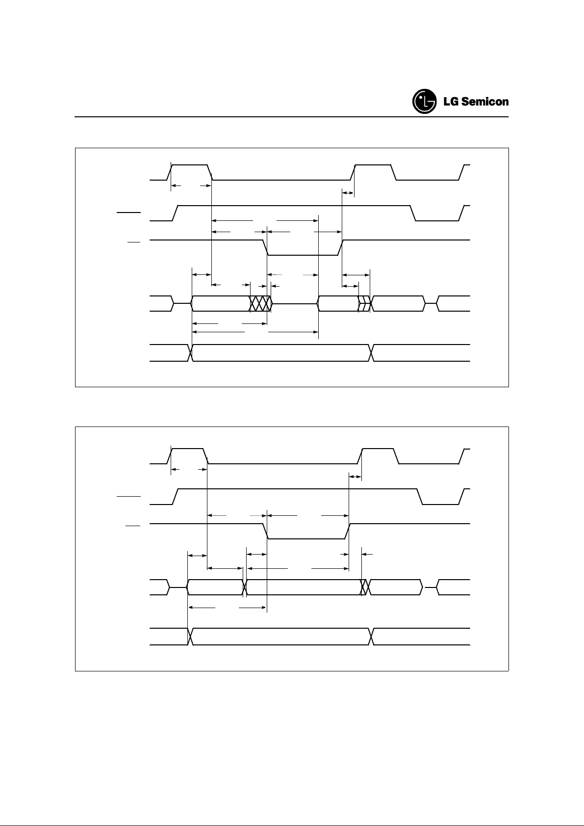
Figure 5. External Data Memory Read Cycle
ALE
t
LHLL
t
AVDV
LLDV
t
RLAZ
t
RLDV
t
RLRH
t
WHLH
t
RHDZ
t
RHDX
DATA IN A0-A7 from PCL INSTR. IN
A8-A15 from PCH
t
WHLH
PSEN
t
LLWL
t
WLWH
WR
t
t
LLAX2
A0-A7 from
RI or DPL
t
AVWL
QVWX
P2.0-P2.7 or A8-A15 from DPH
t
QVWH
DATA OUT
t
WHQX
A0-A7 from PCL
A8-A15 from PCH
INSTR. IN
PORT 0
PORT 2
t
AVLL
Figure 6. External Data Memory Write Cycle
Dec. 1998 Ver 3.0 43
Page 48
GMS90 Series
0.5V
V
−
CC
0.45V
0.2VCC + 0.9
Test Points
− 0.1
0.2V
CC
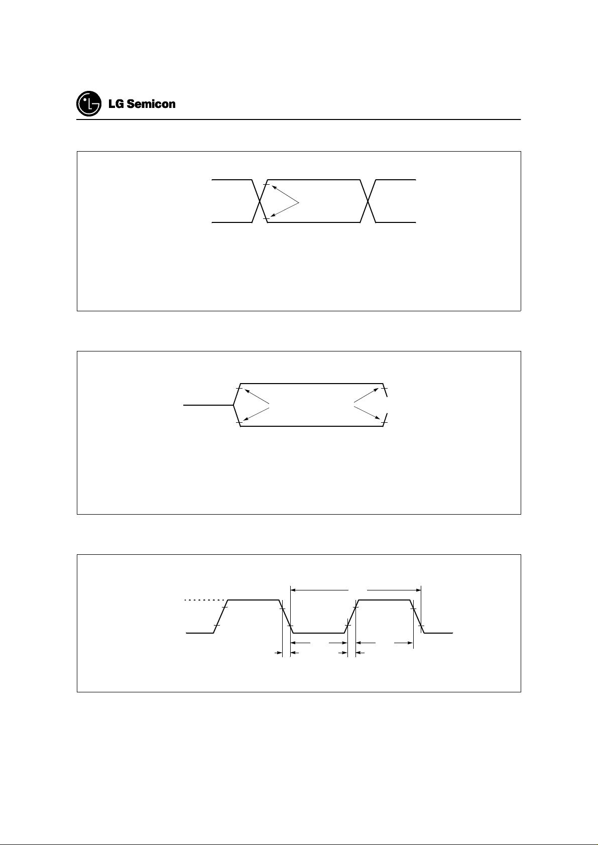
AC Inputs during testing are driven at V
Timing measurements are made a V
−
0.5V for a logic ‘1’ and 0.45V for a logic ‘0’.
CC
for a logic ‘1’ and V
IHmin
for a logic ‘0’.
ILmax
Figure 7. AC Testing: Input, Output Waveforms
0.1
V
−
OH
V
+ 0.1
OL
V
LOAD
V
V
LOAD
LOAD
+ 0.1
− 0.1
Timing Reference Points
0.2VCC − 0.1
For timing purposes a port pin is no longer floating when a 100mV change from load voltage
occurs and begins to float when a 100mV change from the loaded VOH / VOL level occurs.
IOL / IOH ≥ 20mA.
Figure 8. Float Waveforms
t
t
CLCH
CLCL
t
CLCX
0.5V
V
−
CC
0.45V
0.7 V
0.2 V
CC
CC
0.1
−
t
CHCX
t
CHCL
Figure 9. External Clock Cycle
44 Dec. 1998 Ver 3.0
Page 49
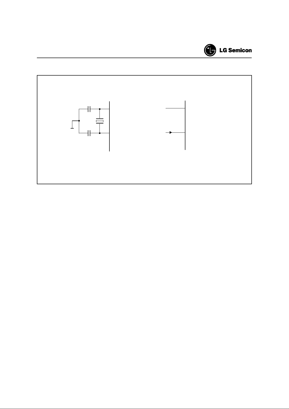
GMS90 Series
OSCILLATOR CIRCUIT
CRYSTAL OSCILLATOR MODE DRIVING FROM EXTERNAL SOURCE
C2
C1
XTAL2
P-LCC-44/Pin 20
P-DIP-40/Pin 18
M-QFP-44/Pin 14
XTAL1
P-LCC-44/Pin 21
P-DIP-40/Pin 19
M-QFP-44/Pin 15
N.C.
External Oscillator
Signal
XTAL2
P-LCC-44/Pin 20
P-DIP-40/Pin 18
M-QFP-44/Pin 14
XTAL1
P-LCC-44/Pin 21
P-DIP-40/Pin 19
M-QFP-44/Pin 15
C1, C2 = 30pF ±10pF for Crystals
For Ceramic Resonators, contact resonator manufacturer.
Figure 10. Recommended Oscillator Circuits
Oscillation circuit is designed to be used either with a ceramic reson ator or crystal oscillator. Sin ce each crystal
and ceramic resonator have th eir own characteristics, the user sho uld consult the cry stal manufacturer for appropriate values of external components.
Dec. 1998 Ver 3.0 45
Page 50
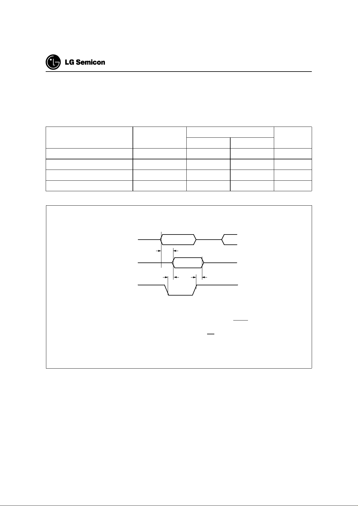
OTP ROM Verification Characteristics
ROM Verification Mode 1
GMS90 Series
Parameter Symbol
Address to valid data
ENABLE to valid data
Data float after ENABLE
Oscillator frequency
P1.0-P1.7
P2.0-P2.4
PORT 0
P2.7
ENABLE
t
AVQV
t
CLCL
t
EHQZ
1/t
t
ELQV
CLCL
Address
t
AVQV
Data Out
Limit Values
Unit
Min. Max.
-48t
-48t
048t
CLCL
CLCL
CLCL
ns
46MHz
t
EHQZ
Address:
Data:
P1.0-P1.7 = A0-A7
P2.0-P2.5 = A8-A13
P3.4 = A14
P0.0-P0.7 = D0-D7
Input:
P2.6-P2.7, PSEN = V
ALE = V
EA, RESET = V
SS
IH
IH2
Figure 11. OTP ROM Verification Mode 1
46 Dec. 1998 Ver 3.0
Page 51
GMS90 Series
EPROM CHARACTERISTICS
The GMS97C5X, 97L5X are programmed by using a modified Quick-Pulse ProgrammingTM algorithm. It differs from older methods in the value used for V
of the ALE/PROG
pulses. The GMS97C5X, 97 L5X c on tai ns two si gnat ur e by tes t hat can be rea d and u sed by
an EPROM programming system to identify the device. The signature bytes identify the device as an manufactured by LGS. Table 11 shows the logic leve ls for reading the signa ture byte, a nd for progra mming the program
memory, the encryption table, and the security bits. The circuit configuratio n and waveforms for quick-pulse
programming are shown in Figu re 12 and Figu re 13. Figure 14 show the circ uit configur ation for norm al program memory verification.
Reading the Signature Bytes :
(programming supply voltage) and in the width and number
PP
The GMS97X51/52 signature byte s in lo catio ns 030
tions 030
and 060H. To read these bytes follow the procedure for EPROM verify, except that P3.6 and P3.7
H
and 031H, the GMS97X54/56/58 signature bytes in loca-
H
need to be pulled to a logic low.
The values are:
Device Location Contents Remarks
GMS97X51 30
31
GMS97X52 30
31
GMS97X54 30
60
GMS97X56 30
60
GMS97X58 30
60
H
H
H
H
H
H
H
H
H
H
E0
73
E0
71
E0
54
E0
56
E0
58
H
H
H
H
H
H
H
H
H
H
Manufacturer ID
Device ID
Manufacturer ID
Device ID
Manufacturer ID
Device ID
Manufacturer ID
Device ID
Manufacturer ID
Device ID
Quick-pulse programming
The setup for microcontroller quick-pulse programming is shown in Figure 13. Note that the GMS97C5X,
97L5X is running with a 4 to 6MHz oscillator. The reason the oscillator needs to be running is that the device
is executing internal address and program data transfers.
The address of the EPROM location to be programmed is applied to ports 1 and 2, as shown in Figure 12. The
code byte to be programmed into that location is applied to port 0, RST, PSEN
11 are held at the "Program Code Data" level s indicated in Tab le 11. The ALE/PROG
and pins of port 2 and 3 in Ta ble
is pulsed low 25 times(10
times for 97X54/56/58) as shown Figure 13.
To program the encryption table, repeat the 25 pulses (10 pulses for 97X54/56/58) programming sequence for
addresses 0 through 1F
(3FH for 97X54/56/58), using the "Program Encryption Table" levels. Do not forget
H
that after the encryption table is programmed, verificatio n cy cles will produce only encrypted data.
To program the security bits, repeat the 25 pulses (1 0 pulses fo r 97X54/56/58) pro gramming seq uence using the
"Pgm Security Bit" levels after one security bit is programmed, further programming of the code memory and
Dec. 1998 Ver 3.0 47
Page 52
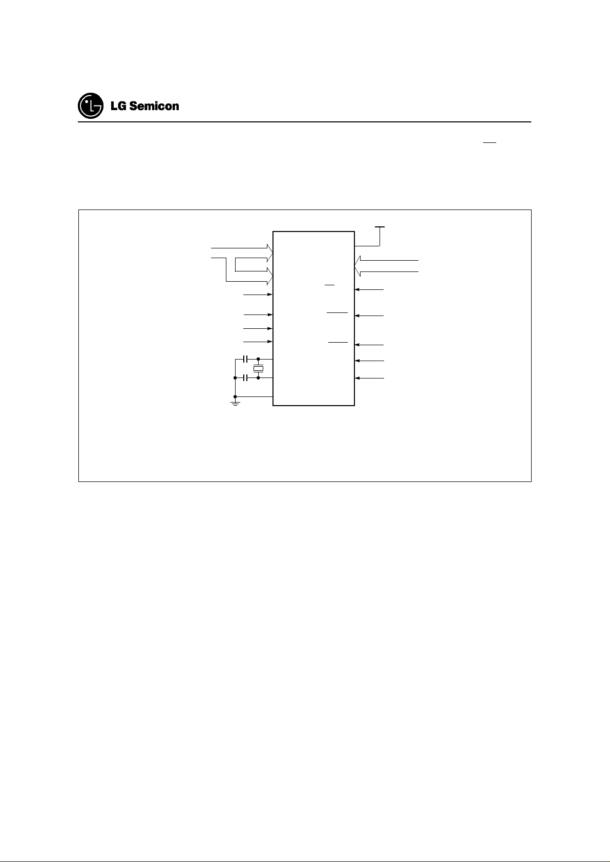
GMS90 Series
encryption table is disabled. However, the other security bit can still be programmed. Note that the EA/VPP pin
must not be allowed to go above the maximum specified V
above that voltage can cause perman ent damage to the de vice. The V
glitches and overshoot.
A0-A7
A8-A13
A14
P1
P2.0
-P2.5
P3.4
level for any amount of time. Even a narrow glitch
PP
source should be well regulated an d free
PP
+5V
V
CC
PROGRAM DATA
P0
EA
/V
PP
+12.75V
4~6MHz
1
1
1
RST
P3.6
P3.7
XTAL2
XTAL1
V
SS
ALE/PROG
PSEN
P2.7
P2.6
☞
0
1
1
NOTE
NOTE:
GMS97X51/52:
GMS97X54/56/58:
100µs × 25 pulses to GND
100µs × 10 pulses to GND
Figure 12. Programming Configuration
Program Verification
If security bit 2 has not been programmed, the on-chip program memory can be read out for program verification. The address of the program memory location to be read is applied to ports 1 and 2 as shown in Figure 15.
The other pins are held at the "Ve rify C ode D ata" levels in dica ted in Ta ble 11. Th e c ontents of the addre ss location will be emitted on port 0 for this operation. If the encryption table has been programmed, the data presented at port 0 will be the exclusive NOR of the program byte with one of the encryption bytes. The user will
have to know the encryption table contents in order to correctly decode the verification data. The encryption
table itself cannot be read out.
48 Dec. 1998 Ver 3.0
Page 53
GMS90 Series
Program Memory Lock Bits
The two-level Program Lock system consists of 2
Lock Bit Protection Modes
Mode LB1 LB2 Protection Type
Lock bits and a 32-byte (64-byte for GMS97X54/
56/58) Encryption Array which are used to protect
the program memory against software piracy.
Encryption Array:
Within the EPROM array are 32 bytes (64 bytes
for GMS97X54/56/58) of Encryption Array that
1 U U No program lock features
2 P U Further programming of the
EPROM is disabled
3 P P Same as mode 2, also verify is
disabled
U: unprogrammed, P: programmed
are initially unprogrammed (all 1s). Every time
that a byte is addressed during a verify, address
lines are used to select a byte of the Encryption array. This byte is then exclusive-NORed (XNOR) with the code
byte, creating an Encrypted Verify byte.
The algorithm, with the array in the unprogrammed state (all 1s), will return the code in its o riginal, unmodified
form, It is recommended that whenever the Encryption Array is used, at least on e of the Lock Bits be programmed as well.
Program / Verify algorithms
Any algorithm in agreement with the conditions listed in Tab le 11, and whi ch satisfies the timing specifications
is suitable.
Table 11. EPROM programming modes
MODE
Read Signature 10110000
Program Code Data
Verify Code Data 10110011
Program encryption table
Program security bit 1
Program security bit 2
Notes:
1. “0” = Valid low for that pin, "1" = valid high for that pin.
2. VPP = 12.75V ± 0.25V
3. VCC = 5V ± 10% during programming and verif icati o n.
4. ALE/PROG receives 25 (10 for GMS97X54/56/58) programming pulses while VPP is held at 12.75V.
Each programming pulse is low for 100us (± 10us) and high for a minimum of 10µs.
RST PSEN
100VPP1011
100VPP1010
100VPP1111
100VPP1100
ALE/
PROG
EA/
V
PP
P2.7 P2.6 P3.7 P3.6
Dec. 1998 Ver 3.0 49
Page 54
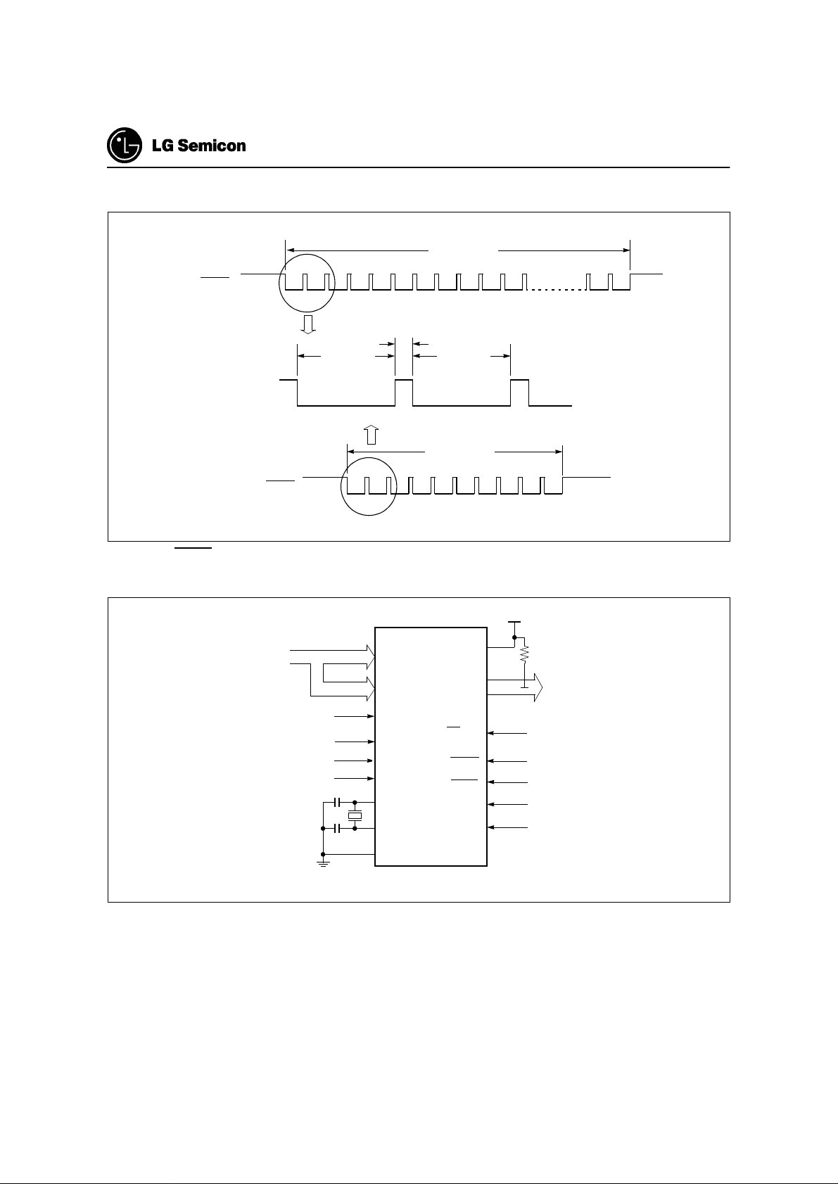
GMS90 Series
In the GMS97X51/52
ALE/PROG
Enlarged View
In the GMS97X54/56/58
ALE/PROG
Figure 13. PROG Waveform
100µs ±10
A0-A7
Min. 10µs
P1
25 PULSES
100µs ±10
10 PULSES
V
CC
+5V
10k
Ω
4~6MHz
A14
1
1
1
A8-A13
P2.0
-P2.5
P3.4
RST
P3.6
P3.7
XTAL2
XTAL1
V
SS
P0
EA
/V
ALE/PROG
PSEN
P2.7
P2.6
PP
PROGRAM DATA
1
1
0
0
1
Figure 14. Program Verification
50 Dec. 1998 Ver 3.0
Page 55
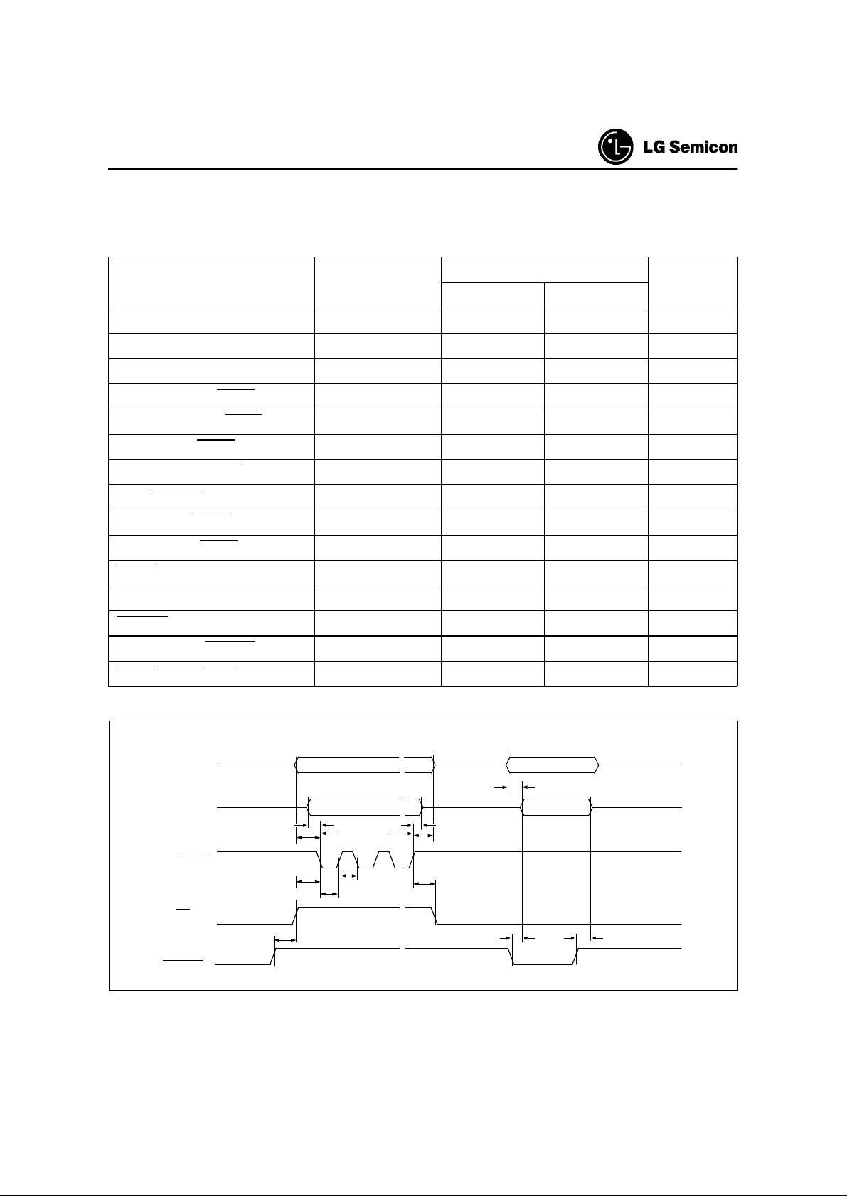
GMS90 Series
EPROM Programming and Verification Characteristics
T
= 21°C to 27°C, VCC= 5V + 10%, − 15%; VSS=0V;
A
Parameter Symbol
Programming supply voltage
Programming supply current
Oscillator frequency
Address setup to PROG low
Address hold after PROG
Data setup to PROG
Data hold after PROG
P2.7 (ENABLE) high to V
PP
VPP setup to PROG t
VPP hold after PROG t
PROG width
Address to data valid
ENABLE low to data valid
Data float after ENABLE
PROG high to PROG low
V
I
1/t
t
AVGL
t
GHAX
t
DVGL
t
GHDX
t
EHSH
SHGL
GHSL
t
GLGL
t
AVQV
t
ELQV
t
EHQZ
t
GHGL
PP
PP
CLCL
Limit Values
Unit
Min. Max.
12.5 13.0 V
-50mA
46MHz
48t
48t
48t
48t
48t
CLCL
CLCL
CLCL
CLCL
CLCL
--
--
--
--
-10 - µs
10 - µs
90 110 µs
-48t
-48t
048t
CLCL
CLCL
CLCL
-
-
-
10 - µs
P1.0-P1.7
P2.0-P2.5
P3.4
PORT 0
ALE/PROG
EA/V
P2.7
(ENABLE)
PP
TTL HIGH
t
EHSH
t
DVGL
t
AVGL
t
SHGL
PROGRAMMING VERIFICATION
ADDRESS
DATA IN
25 or 10
PULSES
t
GLGL
t
V
GHGL
PP
~
~
~
~
t
t
GHDX
t
GHAX
t
GHSL
AVQV
TTL HIGH
t
ELQV
~
~
~
~
~
~
~
~
~
~
ADDRESS
DATA OUT
TTL HIGH
t
EHQZ
Figure 15. EPROM Programming and Verification
Dec. 1998 Ver 3.0 51
Page 56
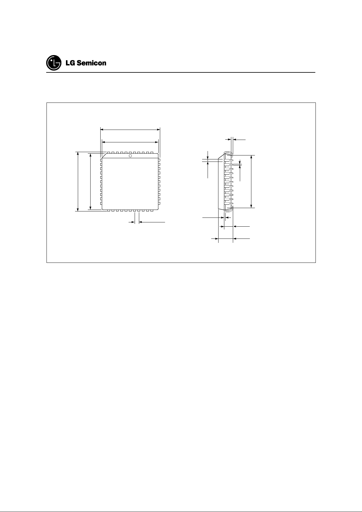
Plastic Package P-LCC-44
(Plastic Leaded Chip-Carrier)
44PLCC
0.656
0.650
0.695
0.685
0.695
0.685
0.656
0.650
0.032
0.026
UNIT: INCH
min. 0.020
0.021
0.013
0.630
0.590
GMS90 Series
0.050 BSC
0.012
0.0075
0.120
0.090
0.180
0.165
52 Dec. 1998 Ver 3.0
Page 57
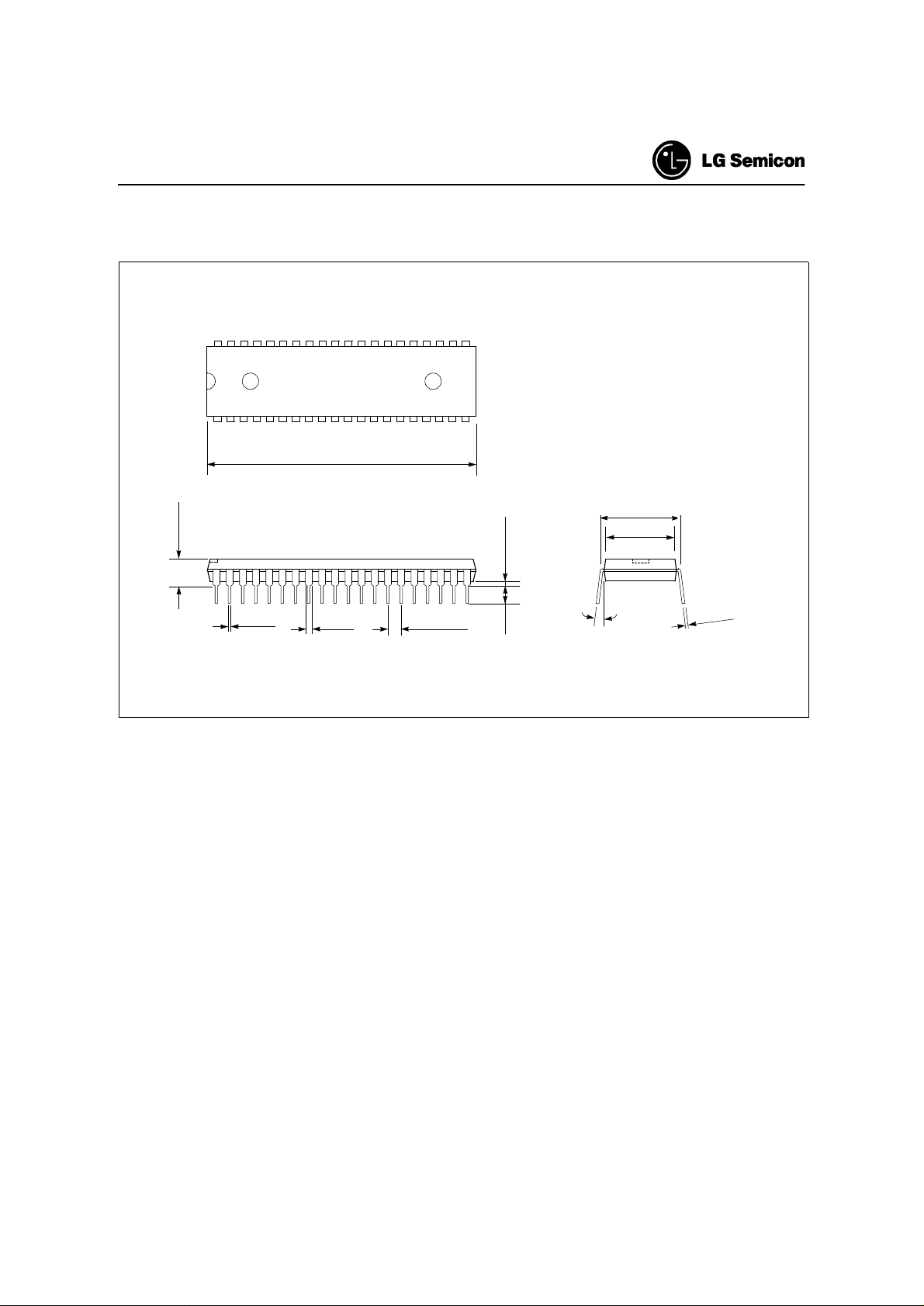
GMS90 Series
Plastic Package P-DIP-40
(Plastic Dual in-Line Package)
40DIP
0.200 max.
0.022
0.015
2.075
2.045
0.065
0.045
0.100 BSC
min. 0.015
0.140
UNIT: INCH
0.600 BSC
0.550
0.530
2
1
0
.
0
8
0
0
.
0.120
0-15
°
0
Dec. 1998 Ver 3.0 53
Page 58
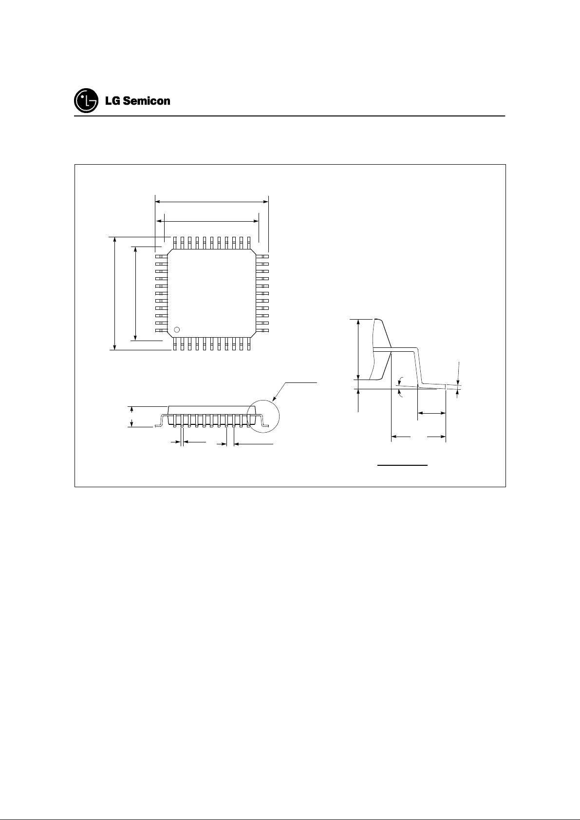
Plastic Package P-MPQF-44
(Plastic Metric Quad Flat Package)
44MQFP
13.45
12.95
10.10
9.90
10.10
13.45
12.95
9.90
SEE DETAIL "A"
2.10
1.95
UNIT: MM
0-7
°
GMS90 Series
3
3
2
1
.
.
0
0
2.35 max.
0.45
0.30
0.80 BSC
0.25
0.10
1.60
REF
DETAIL "A"
1.03
0.73
54 Dec. 1998 Ver 3.0
Page 59
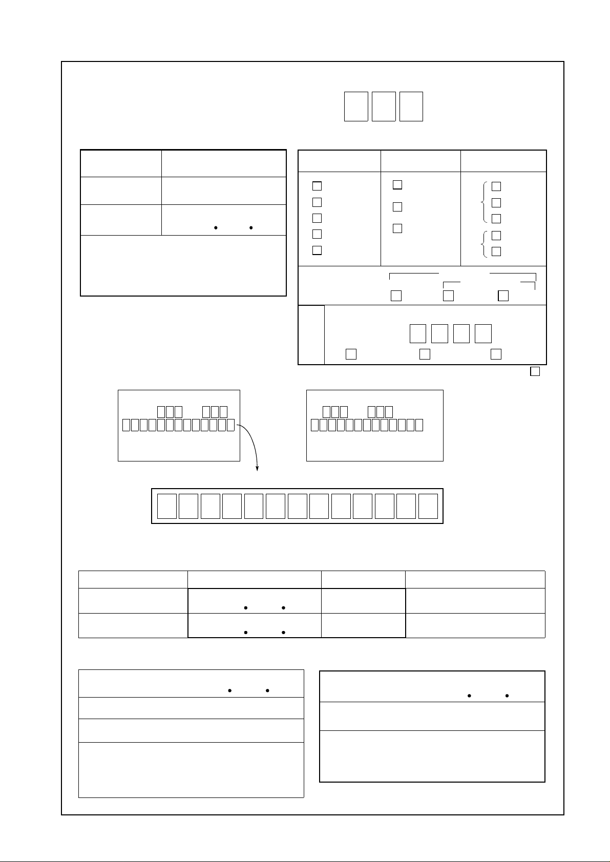
MASK ORDER & VERIFICATION SHEET
GMS90X5X-GB
Customer should write inside thick line box.
1. Customer Information
2. Device Information
Company Name
Application
YYYY MM DD
Order Date
Tel:
Fax:
Name &
Signature:
3. Marking Specification
40PD IP or 44PLCC 44M Q FP
LGS
5
GMS90
-G B
➀➁
Y Y WW K O RE A
SIEMENS ’92
ROM size
4K
8K
16K
24K
32K
ROM Protection
File Name: ( .HEX)
Check Sum:
Mask Data
LGS
5
➀
➁
-G B
90
Y Y WW K O RE A
SIEMENS ’92
Package
44MQFP
44PLCC
40PDIP
Without
Vol. / Freq.
12MHz
5V
3V
ROM: 4K,8K
ROM: 16,24,32K
Normal Super
(Please check mark into )
➀
C: 5V
L: 3V
24MHz
40MHz
12MHz
16MHz
HitelChollianInternet
ROM size
➁
1: 4K
2: 8K
4: 16K
6: 24K
8: 32K
Customer’s part number
4. Delivery Schedule
Customer Sample
Risk Order
YYYY MM DD
YYYY MM DD
5. ROM Code Verification
Ve rific a tio n Da te :
YYYY MM DD
Please confirm our verification data.
Check Sum:
Tel:
Fax:
Name &
Signature:
Date
Quantity
LG Confirmation
pcs
pcs
This box is written after “5.Verification”.
YYYY MM DD
Approval Date:
I agree with your verification data and confirm you to
make mask set.
Tel:
Fax:
Name &
Signature:
LG Semicon
 Loading...