

Page 1

GMS81508A
GMS81516A
USER’S MANUAL
Revision History
Rev 2.2 (Dec. 1998)
Add the package dimension for 64LQFP on page 3-1, 4-1.
Rev 2.1 (Nov. 1998)
Operating Temperature, -10~75°C is extended to -20~85°C.
Add the unused port guidance on page 55.
Correct errata for opcode of “EOR [dp+X], EOR [dp]+Y, EOR {X}” in “Instruction Set”.
Add the OTP device programming guidance, recommend using “Intelligent Mode”.
Add the chapter for OTP programming manual as an appendix.
Rev 2.0 (Sep. 1997)
Page 2

- CONTENTS -
1. OVERVIEW...........................................................................................................................................1
1.1. FEATURES..........................................................................................................................................1
1.2. BLOCK DIAGRAM..............................................................................................................................2
1.3. PIN ASSIGNMENT ..............................................................................................................................3
1.4. PACKAGE DIMENSION .....................................................................................................................4
1.5. PIN DESCRIPTION..............................................................................................................................5
2. FUNCTIONS..........................................................................................................................................7
2.1. REGISTERS.........................................................................................................................................7
2.1.1. A - Register....................................................................................................................................8
2.1.2. X- Register.....................................................................................................................................8
2.1.3. Y- Register.....................................................................................................................................8
2.1.4. Stack Pointer .................................................................................................................................8
2.1.5. Program Counter.........................................................................................................................10
2.1.6. Program Status Word...................................................................................................................10
2.2. MEMORY SPACE..............................................................................................................................12
2.2.1. RAM area....................................................................................................................................12
2.2.2. Peripheral Register area..............................................................................................................12
2.2.3. Progr a m ROM area.....................................................................................................................12
2.2.4. Peripheral Register List ...............................................................................................................14
2.3. CLOCK GENERATION CIRCUIT.....................................................................................................16
2.3.1. Oscillation Circuit .......................................................................................................................16
2.3.2. Prescaler.....................................................................................................................................17
2.4. BASIC INTERVAL TIMER................................................................................................................18
2.4.1. Control of Basic Interval Timer....................................................................................................18
2.5. WATCH DOG TIMER........................................................................................................................ 19
2.5.1. Control of Watch Dog Timer........................................................................................................19
2.5.2. The output of WDT signal.............................................................................................................20
2.6. TIMER................................................................................................................................................21
2.6.1. Control of Timer .......................................................................................................................... 23
2.6.2. Interval Timer..............................................................................................................................24
2.6.3. Event Counter..............................................................................................................................24
2.6.4. Pulse Output................................................................................................................................ 24
2.6.5. Input Capture...............................................................................................................................24
2.7. EX TERNA L INTERRUPT..................................................................................................................26
2.8. A/D CONVERTER ............................................................................................................................. 27
2.8.1. Control of A/D Converter.............................................................................................................27
2.9. SERIAL I/O........................................................................................................................................29
2.9.1. Data Transmission/Receiving Timing...........................................................................................31
2.9.2. The Serial I/O operation by Srdy pin ............................................................................................ 31
2.9.3. The method of Serial I/O..............................................................................................................32
2.9.4. The Method to Test Correct Transmission with S/W......................................................................32
2.10. PWM ................................................................................................................................................33
2.10.1. Controls of PWM ....................................................................................................................... 33
2.11. BUZZER DRIVER............................................................................................................................35
2.11.1. Buzzer Driver Operation............................................................................................................36
2.12. INTERRUPTS...................................................................................................................................37
2.12.1. Interrupt Circuit Configuration and Kinds ..................................................................................37
2.12.2. Interrupt Control........................................................................................................................38
2.12.3. Interrupt Priority ..................................................................................................... ..................39
Page 3

2.12.4. Interrupt Sequence.....................................................................................................................40
2.12.5. Software Interrupt ..................................................................................................................... 41
2.12.6. Multiple Interrupt...................................................................................................................... 42
2.13. STANDBY FUNCTION...................................................................................................................44
2.13.1. STOP Mode............................................................................................................................... 45
2.13.2. STOP Mode Release.................................................................................................................. 45
2.14. RESET FUNCTION......................................................................................................................... 47
3. I/O PORTS...........................................................................................................................................48
3.1. R0 PORT............................................................................................................................................ 48
3.2. R1 PORT............................................................................................................................................ 49
3.3. R2 PORT............................................................................................................................................ 50
3.4. R3 PORT............................................................................................................................................ 51
3.5. R4 PORT............................................................................................................................................ 52
3.6. R5 PORT............................................................................................................................................ 53
3.7. R6
PORT............................................................................................................................................ 54
3.8. TERMINA L TYPES........................................................................................................................... 56
4. ELECTRICAL CHARACTERISTICS............................................................................................... 60
4.1. ABOULUTE MAXIMUM RATINGS.................................................................................................60
4.2. RECOMMENDED OPERATING CONDITIONS............................................................................... 60
4.3. A/D CONVERTER CHARACTERISTICS .........................................................................................60
4.4. DC CHARACTERISTICS........................................................................................................ .......... 61
4.5. AC CHARACTERISTICS........................................................................................................ .......... 62
4.5.1. Input Conditions.......................................................................................................................... 62
4.5.2. Serial Transfer............................................................................................................................63
4.5.3. Microprocessor Mode I/O Timing................................................................................................64
4.5.4. Bus Holding Timing.....................................................................................................................65
5. INSTRUCTION SET........................................................................................................................... 66
Page 4
GMS81508/16
1
1. OVERVIEW
GMS81508/16 is a singl e c hip mi c r oc om puter designed CMOS technology. The use of CMOS
process enables ext r em ely low power consumption.
This devic e using the G8MC Cor e incl udes several peripheral functions such as Timer, A/D
Converter, Programmable Buzzer Driver, Serial I/ O, P ulse Width Modulation Function, et c.
ROM,RAM,I/O are plac ed on the same memory map in addition to simple instruc tion set.
1.1. FEATURES
GMS81508 GMS81516
ROM(Bytes)
8K 16K
RAM(Bytes)
448 bytes(includes stack area)
Execution Time
0.5us (@Xin=8MHz )
Basic Interval Timer
8bit ✕ 1ch.
Watch Dog Timer
6bit ✕ 1ch.
Timer
8bit✕4ch.(or 16bit ✕ 2ch.)
ADC
8bit ✕ 8ch.
PWM
8bit ✕ 2ch.
Serial I/O
8bit ✕ 1ch.
External Interrupt
4ch.
Buzzer Driver
Programmable B uzzer Driving Port
I/O Port
4 - Input only
52 - Input/Output
Power Save Mode
STOP Mode
Operating Volt age
4.5 ∼ 5.5V ( @ Xin=8MHz )
Operating Frequ ency
1 ∼ 8MHz
Package
64SDIP, 64QFP
OTP
GMS81516T
Application
Home Appliances, LED Applications
Page 5
HYUNDAI MicroElectronics
2
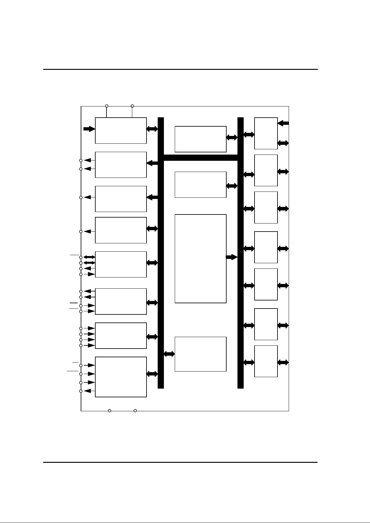
1.2. BLOCK DIAGRAM
A/D
CONVERTER
PWM
BUZZER
W.D.T
S.I.C
TIMER
INTERRUPT
CLOCK GEN.
/
SYSTEM
CONTROL
G8MC
CORE
RAM
(448 BYTE)
ROM
(8/16K BYTE)
PRESCALER
/
B.I.T
R6
PORT
R5
PORT
R4
PORT
R3
PORT
R2
PORT
R1
PORT
R0
PORT
AVref AVss
R60~R67
(AN0~AN7)
R57/PWM1
R55/BUZ
R56/PWM0
R54/WDTO
R53/Srdy
R52/Sclk
R51/Sout
R50/Sin
R47/T3 O
R46/T1 O
R45/EC2
R44/EC0
R43/INT3
R42/INT2
R41/INT1
R40/INT0
MP
RESET
Xin
Xout
Vdd Vss
R60
:
R63
R64
:
R67
R50
:
R57
R40
:
R47
R30
:
R37
R20
:
R27
R10
:
R17
R00
:
R07
Page 6
GMS81508/16
3
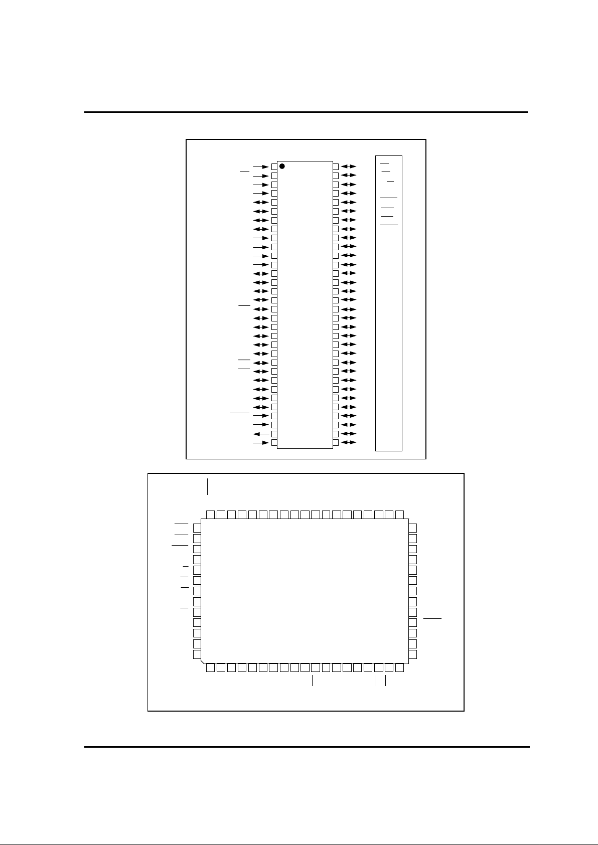
1.3. PIN ASSIGNMENT
G
M
S
8
1
5
0
8
/
1
6
R30/ RD
R31/ Wt
R32/ R/W
R33/ C
R34/ SYNC
R35/ BRK
R36/ BRQ
R37/ HALT
R00/ D0
R01/ D1
R02/ D2
R03/ D3
R04/ D4
R05/ D5
R06/ D6
R07/ D7
R10/ A0
R11/ A1
R12/ A2
R13/ A3
R14/ A4
R15/ A5
R16/ A6
R17/ A7
R20/ A8
R21/ A9
R22/ A10
R23/ A11
R24/ A12
R25/ A13
R26/ A14
R27/ A15
Vdd
MP
AVss
AVref
R67/AN7
R66/AN6
R65/AN5
R64/AN4
R63/AN3
R62/AN2
R61/AN1
R60/AN0
R57/PWM1
R56/PWM0
R55/BUZ
R54/WDTO
R53/Srdy
R52/Sclk
R51/Sout
R50/Sin
R47/T3O
R46/T1O
R45/EC2
R44/EC0
R43/INT3
R42/INT2
R41/INT1
R40/INT0
RESET
Xin
Xout
Vss
1
2
3
4
5
6
7
8
9
10
11
12
13
14
15
16
17
18
19
20
21
22
23
24
25
26
27
28
29
30
31
32
64
63
62
61
60
59
58
57
56
55
54
53
52
51
50
49
48
47
46
45
44
43
42
41
40
39
38
37
36
35
34
33
MP MODE
64 SDIP
GMS81508/16
R65/AN5
R64/AN4
R63/AN3
R62/AN2
R61/AN1
R60/AN0
R57/PWM1
R56/PWM0
R55/BUZ
R54/WDTO
R53/Srdy
R52/Sclk
R51/Sout
R50/Sin
R47/T3O
R46/T1O
R45/EC2
R44/EC0
R43/INT3
21
31 2 4 5 6 7 8 9 10 11 12 13 14 15 16 17 18 19
22
23
24
25
26
27
28
29
30
31
32
20
4951 50 48 47 46 45 44 43 42 41 40 39 38 37 36 35 34 33
63
62
61
60
59
58
57
56
55
54
53
52
64
R37/HALT
R00/D0
R01/D1
R02/D2
R03/D3
R04/D4
R05/D5
R06/D6
R07/D7
R10/A0
R11/A1
R12/A2
R13/A3
R14/A4
R15/A5
R16/A6
R17/A7
R20/A8
R21/A9
R22/A10
R23/A11
R24/A12
R25/A13
R26/A14
R17/A15
Vss
Xout
Xin
RESET
R40/INT0
R41/INT1
R42/INT2
R36 BRQ
R35 BAK
R34 SYNC
R33 C
R32 R/W
R31 Wt
R30 Rd
Vdd
MP
AVss
AVref
R67/AN7
R66/AN6
64 QFP
Page 7
HYUNDAI MicroElectronics
R20
R21
R22
R23
R24
R25
R26
R27
VSS
XOUT
XIN
RESET
R40/INT0
R41/INT1
R42/INT2
R43/INT3
R00
R01
R02
R03
R04
R05
R06
R07
R10
R11
R12
R13
R14
R15
R16
R17
R63/AN3
R62/AN2
R61/AN1
R60/AN0
R57/PWM1
R56/PWM0
R55/BUZ
R54/WDTO
R53/SRDY
R52/SCLK
R51/SOUT
R50/SIN
R47/T3O
R46/T1O
R45/EC2
R44/EC0
123456789
10111213141516
R37
R36
R35
R34
R33
R32
R31
R30
VDD
MP
AVSS
AVREF
R67/AN7
R66/AN6
R65/AN5
R64/AN4
484746454443424140393837363534
33
32
31
30
29
28
27
26
25
24
23
22
21
20
19
18
17
49
50
51
52
53
54
55
56
57
58
59
60
61
62
63
64
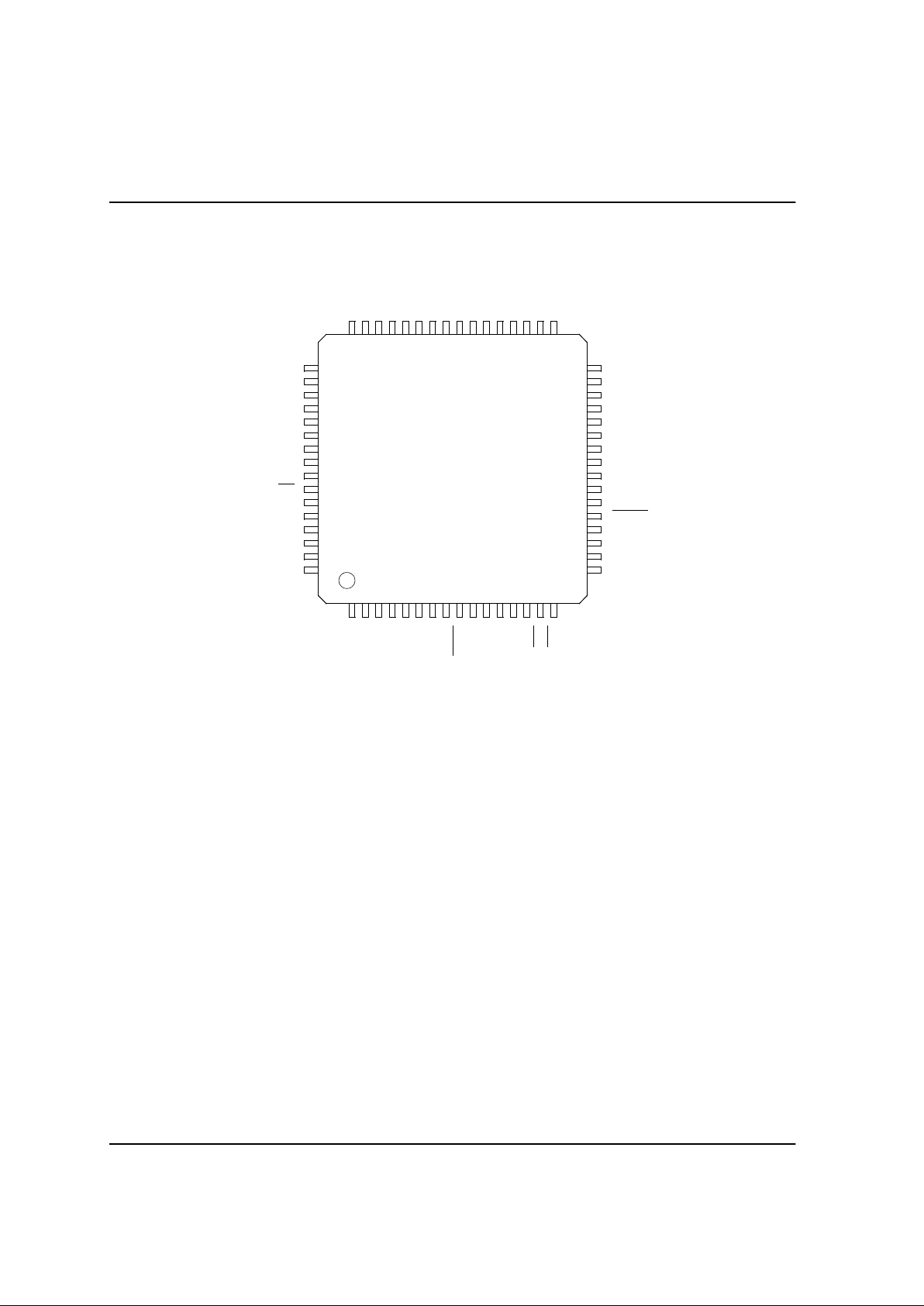
GMS81508/16
64LQFP
3-1
Page 8
HYUNDAI MicroElectronics
4
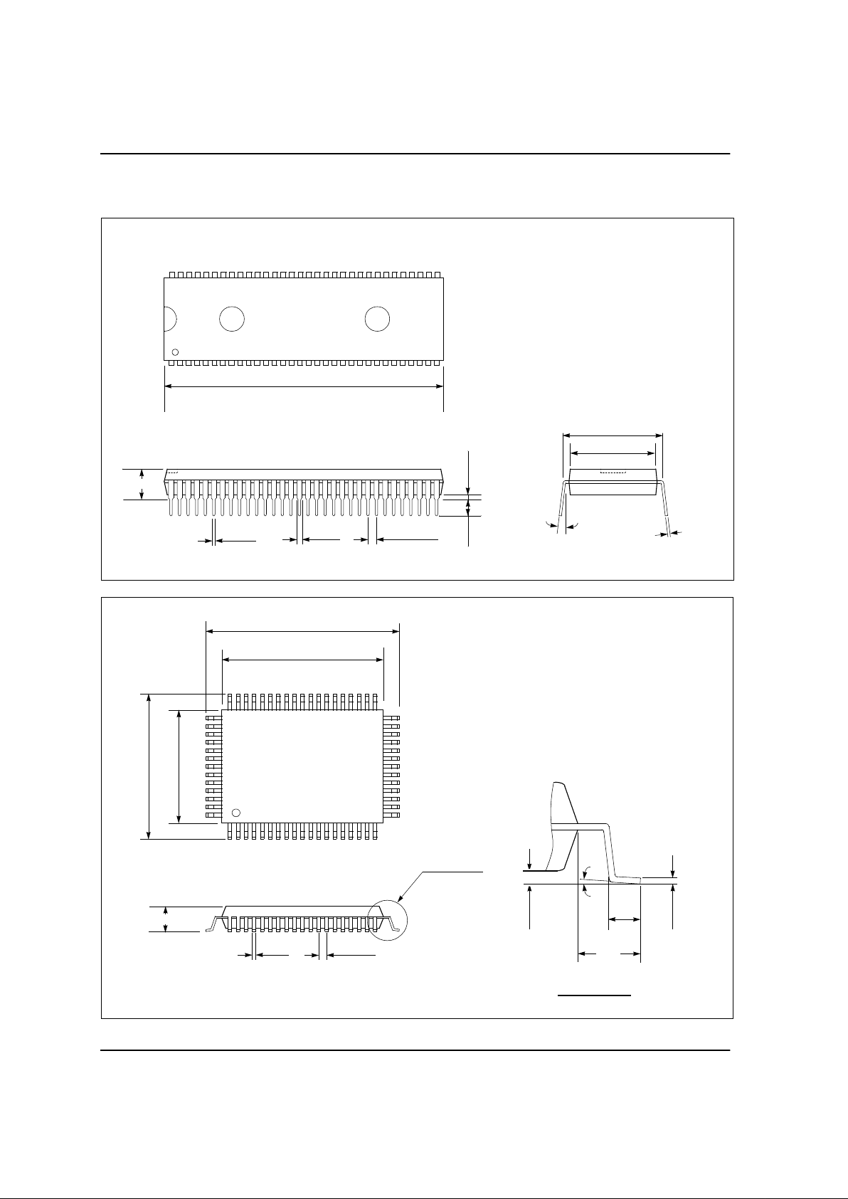
1.4 PACKAGE DIMENSION
UNIT: INCH
2.280
2.260
0.205 max.
0.022
0.016
0.050
0.030
0.070 BSC
0.140
0.120
min. 0.015
0.680
0.660
0.750 BSC
0-15
°
0.012
0.008
64SDIP
20.10
19.90
24.15
23.65
18.15
17.65
14.10
13.90
3.18 max.
0.50
0.35
1.00 BSC
SEE DETAIL "A"
1.03
0.73
0-7
°
0.36
0.10
0.23
0.13
1.95
REF
DETAIL "A"
UNIT: MM
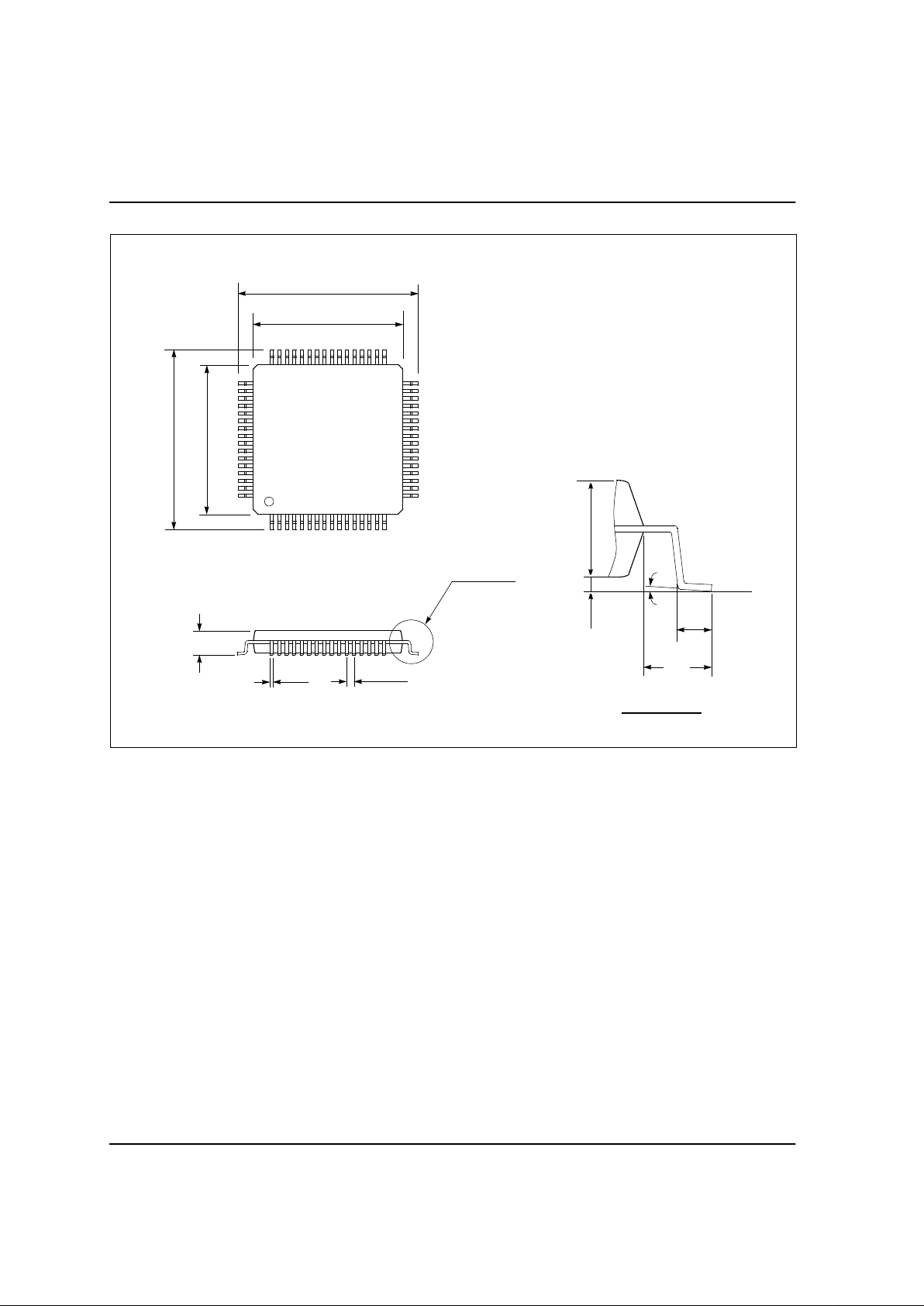
64QFP
Page 9
HYUNDAI MicroElectronics
1.60 max.
SEE DETAIL "A"
0.75
0.45
0-7
°
0.15
0.05
1.00
REF
DETAIL "A"
UNIT: MM
10.00 BSC
12.00 BSC
12.00 BSC
10.00 BSC
0.38
0.22
0.50 BSC
1.45
1.35
64LQFP
4-1
Page 10
GMS81508/16
5
1.5. PIN DESCRIPTION
Classification No. Symbol I/O Descriptions
Power 1 Vdd I Power Supply Input Pi n( 4.5~5.5V)
32 Vss I Ground(0V)
2MP
I Controls Micropr oc ess Mode of the Chip
At "H" input : Single Chip M ode
At "L" input : Microprocess Mode
System Controlor29 RESET I In the state of "L" level, system enter to the reset
state.
Clock
30 Xin
I This chip has an inter nal cl oc k gener ating circuit. To
control gener ating frequency, an external c er ami c or
a quartz crystal oscillator is connected between Xin
and Xout pins.
31 Xout I If external clock is used, the clock source should be
connected to the Xi n pi n and the Xout pin should be
left open.
24 EC0 I Event Counter Source Cloc k Input Pin
Timer 23 EC2 I
22 T1O O Timer Counter Overflow Output Pin
21 T3O O
28 INT0 I
Ext. Interr upt 27 INT 1 I External Inter r upt Request Signal Input Pin
26 INT2 I
25 INT3 I
4 AVref I Referenc e Voltage Input Pin for A/D Converter
3 AVss I Ground Level Input Pin for A/D Converter
12 AN0 I
11 AN1 I
A/D Converter 10 AN2 I
9 AN3 I Analog Voltage Input Pin for A/ D Conv erter
8AN4 I
7AN5 I
6AN6 I
5AN7 I
17 Srdy I/O Receive Enable Output Pin
Serial I/O 18 Sclk I/O Serial Clock Output Pin
19 Sout O Serial Dat a Output Pin
20 Sin I Serial Data Input Pin
P.W.M 14 PWM0 O PWM Pulse Output Pin
13 PWM1 O
Buzzer 15 BUZ O Buzzer Driving Frequency Out put Pin
W.D.T 16 WDTO O Watch dog Timer Overflow Output Pin
Page 11

HYUNDAI MicroElectronics
6
Classification No. Symbol I/O Description
49
:
56
R00
:
R07
I/O
R0 Port
( Can be determined I/O by R0DD )
In MP mode, This port functions as 8-bit data bus for
the CPU. (D0~D7)
41
:
48
R10
:
R17
I/O
R1 Port
( Can be determined I/O by R1DD )
In MP mode, This functions as 8-bit lower address
output pins. (A0~A7)
33
:
40
R20
:
R27
I/O
R2 Port
( Can be determined I/O by R2DD )
In MP mode, This functions as 8-bit higher address
output pins.(A8~A15)
I/O Port 57
:
64
R30
:
R37
I/O
R3 Port
( Can be determined I/O by R3DD )
In MP mode, This port functions as 8-bit control bus
for the CPU.
28
:
21
R40
:
R47
I/O
R4 Port
( Can be determined I/O by R4DD )
20
:
13
R50
:
R57
I/O
R5 Port
( Can be determined I/O by R5DD )
12
:
9
R60
:
R63
I
R6 Port
Input Only
8
:
5
R64
:
R65
I/O R6 Port
( Can be determined I/O by R6DD )
Page 12
GMS81508/16
7
2. FUNCTIONS
2.1. REGISTERS
6 registers are built-in the CPU of G8MC. Accumulator(A) , I ndex regi st er X, Y, Stac k P ointer (SP)
and Program Status Word(PSW) consists of 8-bit registers. P r ogr am Counter(PC) consists of 16bit registers. The contents of these registers are undefined after RESET.
P
rogram Counter
15 8
PCH
7 0
PCL
A
- Register
7 0
A
15 8
Y
( YA 16bit Accumulator )
7 0
A
X
- Register
7 0
X
Y
- Register
7 0
Y
P
rogram Status Word
7 0
PSW
S
tack Pointer
7 0
SP
C
arry Flag
Z CH IG BN V
Z
ero Flag
I
nterrupt Enable Flag
H
alf Carry Flag
B
reak Flag
G
( Direct Page ) Flag
O
verflow Flag
N
egative Flag
Page 13

HYUNDAI MicroElectronics
8
2.1.1. A - Register
The accumulator is the 8-bit general purpose register. This is used register for data oper ation, data
transfer, temporary saves and conditional judgment.
Accumulator can be used as a 16-bit r egister with Y r egister and has a lower 8- bit data.
In case of multiplication instruction(MUL), it wor k s as a multiplier. After exec ution of MUL
instruction, Accumulator has lower 8- bit data of the results(16-bit).
In case of division instruction(DIV), it has the lower 8- bit of dividend (16-bit)
2.1.2. X- Register
In index addressing mode, this register is executed as a 8-bit index register within dir ec t page(RA M
area). also, In indirec t addressing mode, it is destination address register.
This register can be used as a increment, dec r ement, comparison, and data transfer function.
In case of division instruction(DIV), it work s as a divisor .
2.1.3. Y- Register
In index addressing mode, this register is executed as a index register.
In case of 16-bit operation instruction, this register has upper 8- bit of YA (16-bit accumulator) .
In case of multiplication instruction(MUL), this register is exec uted as a multiplicand register. After
multiplication operation, it has the upper 8-bit of the r esult.
In case of division instruction, it is executed as a dividend(upper 8- bit). After division operation, it
has quotient.
This register can be used as a loop counter of conditional branch command. (e.g. DBNE Y , rel)
2.1.4. Stack Pointer
The stack pointer(SP) is an 8-bit register used during subroutine calling and interrupts.
When branching out from an on-going routine to subroutine or interrupt routine, it is necessary to
remember the return address. normally , internal RA M is used for stor ing the retur n addr ess and
this area is called stack area. SP is pointer to show wher e the stac k data ar e stor ed within the
stack area.
The stack area is located in 1-Page of inter nal RAM. SP must be initialized by S/W because the
contents of SP is undefined after RESET.
ex) LDX #0FEH ;0FEH -> X register
TXSP ;X -> SP
caution) You can't use !01FFH as stack. If you use this area, mal-function would be
occurred.
Page 14
GMS81508/16
9
The bellows shows data store and restore s equenc e to/from stack ar ea.
Interrupt
RETI
Subroutine CALL
RET
PUSH A ( X, Y, PSW )
POP A ( X, Y, PSW )
M (sp) ( PCH )
sp sp 1
M (sp) ( PCL )
sp sp 1
M (sp) A
M (sp) ( PCH )
sp sp 1
M (sp) ( PCL )
sp sp 1
M (sp) ( PSW )
sp sp 1
sp sp 1
sp sp 1
( PCL ) M (sp)
sp sp 1
( PCH) M (sp)
sp sp 1
A M (sp)
( PSW ) M (sp)
sp sp 1
( PCL ) M (sp)
sp sp 1
( PCH) M (sp)
sp sp 1
15 8
Stack Address ( 0100
H
01FF
H
)
01
H
7 0
SP
Hardware fixed
Page 15

HYUNDAI MicroElectronics
10
2.1.5. Program Counter
The program counter ( P C) is a 16- bit counter whic h c onsists of 8-bit register PCH and PCL. The
addressing space is 64K bytes.
This counter indicates the address of the next instruction to be executed.
In reset state, the program c ounter (P C) has r eset routine address in address FFFFH and FFFEH .
2.1.6. Program Status Word
PSW is an 8-bit register which is composed of flags to maintain the condition of the processor
immediately after an operation.
After RESET, The contents of P SW is set to "00H".
PSW
Carry Flag ( C )
After an operation, it is set to "1" when there is a car r y fr om bit7 of ALU or not a borrow.
SETC,CLRC instructions allow direct access for setting and r esetting.
it can be used as a 1-bit accumulator.
It is a branch condition flag of BCS, BCC instruc tions.
Zero Flag ( Z )
After an operation including 16-bit operation, it is set to "1" when the result is “ 0” .
It is a branch condition flag of BEQ, B NE .
Interrupt Enable Flag ( I )
This flag is used to enable/disable all interrupts except interrupt caused by B RK instr uc tion.
When this flag is "1", it means interrupt enable condition. When an interrupt is accept, this flag is
automatically set to "0" thereby preventing other interrupts. also it is set to "1" by RETI instruction.
This flag is set and cleared by EI, DI instructions.
Half Carry Flag ( H )
After an operation, it is set when there is a car r y fr om bit3 of ALU or is not a borrow from bit4 of
ALU.
It can not be set by any instr uc tion. it is cleared by CLRV instruction like V flag.
7
N6V5G4B3H
2
I
1
Z0C
Page 16

GMS81508/16
11
Break Flag ( B )
This flag is set by BRK (S/W int er rupt) instruction to disti nguish BRK and TCALL instruction having
the same vector address.
Direct Page Flag ( G )
This flag assign dir ec t page (0- page, 1-page) for direct addressing mode. When G-flag is "0", the
direct addressing space is in 0-page(0000H~00FF H ) . When G-flag is "1", the direct addressing
space is in 1-page(0100H~01FFH).
It is set and cleared by SETG, CLRG instruction
Overflow Flag ( V )
This flag functions when one word is added or subtracted in bi nar y wit h the sign. When results
exceeds +127 or -128, t his flag is set.
When BIT instruction is executed, The bit6 of memory is input into V-flag.
This flag is clear ed by CLRV instruc tion, but set instruction is not ex ist.
It is a branch condition flag of BVS, BVC.
Negative Flag ( N )
N-flag is set when the result of a data transfer or operation is negative (bit7 is “1”).
it means the bit-7 of memor y i s sign bit . t her eby data is valid in the range of -128 ~ +127.
When BIT instruction is executed, The bit7 of memory is input into N-flag.
Set or clear instruc tion is not exist.
It is a branch condition flag of BPL, BMI instruction.
Page 17

HYUNDAI MicroElectronics
12
2.2. MEMORY SPACE
All RAM ,ROM,I/O, Peripheral Register ar e plac ed in the same memor y ar ea. Therefore, same
instructions enable both data transfer and operation without the need to distinguish memory and
I/O. The program c ounter of GMS81508/16 consists of 16-bit and memory addressing space is 64K
byte.
2.2.1. RAM area
RAM(includes stack area) is 448 B ytes ( 0000
H
01FF
H
).
The internal RAM is used for data storage, subroutine calling or stack area when interrupts occ ur .
When RAM is used as the stack area, the depth of the subroutine "nesting" and the interrupt levels
should be kept in mind in order to avoid destruc tion of the RAM c ontents.
2.2.2. Peripheral Register area
Address 00C0
H
00FF
H
are assigned for peripheral register .
2.2.3. Program ROM area
PCALL subroutines must be located in
PCALL
area ( FF00
H
FFBF
H
).
TCALL
vector area ( FFC0
H
FFDF
H
) has the vector address corresponding to TCALL
instruction.
Interrupt Vector
area ( FFE0
H
FFFF
H
) has the vector address of interr upts, inclusive RESET.
Page 18
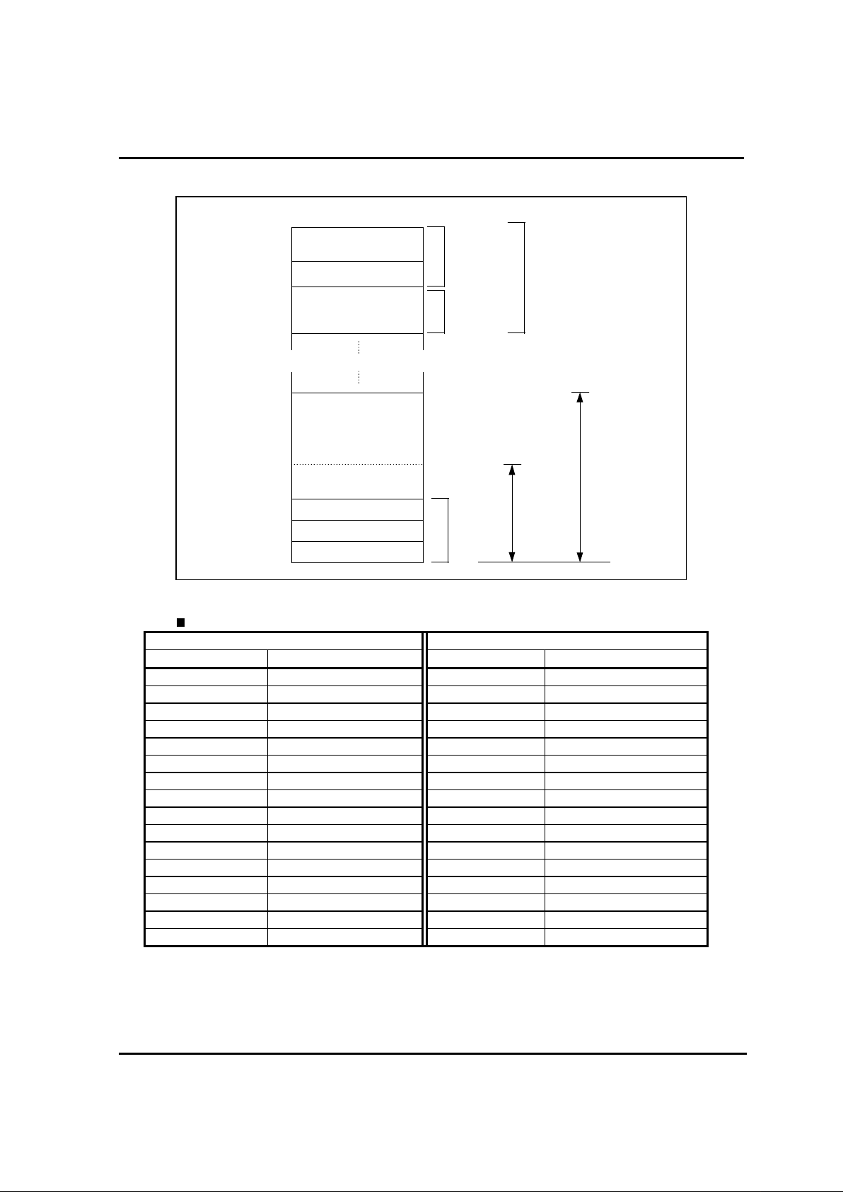
GMS81508/16
13
RAM
(192 byte)
Peripheral Registers
RAM(STACK)
(256 byte)
Program ROM
PCALL Area
TCALL Vector Area
Interrupt Vector Area
!0000H
!00C0H
!0100H
!0200H
!C000H
!E000H
!FF00H
!FFC0H
!FFE0H
Not Used Area
0-Page
1-Page
Direct Page(dp)
U-Page
G
M
S
8
1
5
0
8
G
M
S
8
1
5
1
6
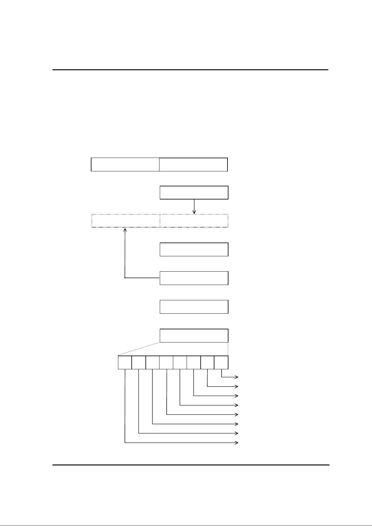
Absolute Address
VECTO R TABL E
TCALL INTERRUPT
Address Vector Address Vector
FFC0H - FFC1H TCALL 15 FFE0H - FFE1H not used
FFC2H - FFC3H TCALL 14 FFE2H - FFE3H not used
FFC4H - FFC5H TCALL 13 FFE4H - FFE5H Serial I/O
FFC6H - FFC7H TCALL 12 FFE6H - FFE7H B asic Interval Timer
FFC8H - FFC9H TCALL 11 FFE8H - FFE9H Watch Dog Timer
FFCAH - FFCBH TCALL 10 FFEAH - FFEBH A/D Converter
FFCCH - FFCDH T CA LL 9 FFECH - FFEDH Tim er 3
FFCEH - FFCFH TCALL 8 FFEEH - FFEFH Timer 2
FFD0H - FFD1H TCALL 7 FFF0H - FFF1H Timer 1
FFD2H - FFD3H TCALL 6 FFF2H - FFF3H Timer 0
FFD4H - FFD5H TCALL 5 FFF4H - FFF5H Ex t. Int. 3
FFD6H - FFD7H TCALL 4 FFF6H - FFF7H Ex t. Int. 2
FFD8H - FFD9H TCALL 3 FFF8H - FFF9H Ex t. Int. 1
FFDAH - FFDBH TCALL 2 FFFAH - FFFBH Ext. Int. 0
FFDCH - FFDDH T CA LL 1 FFFCH - FFFDH not used
FFDEH - FFDFH TCALL 0 FFFEH - FFFFH RESET
Page 19
HYUNDAI MicroElectronics
14
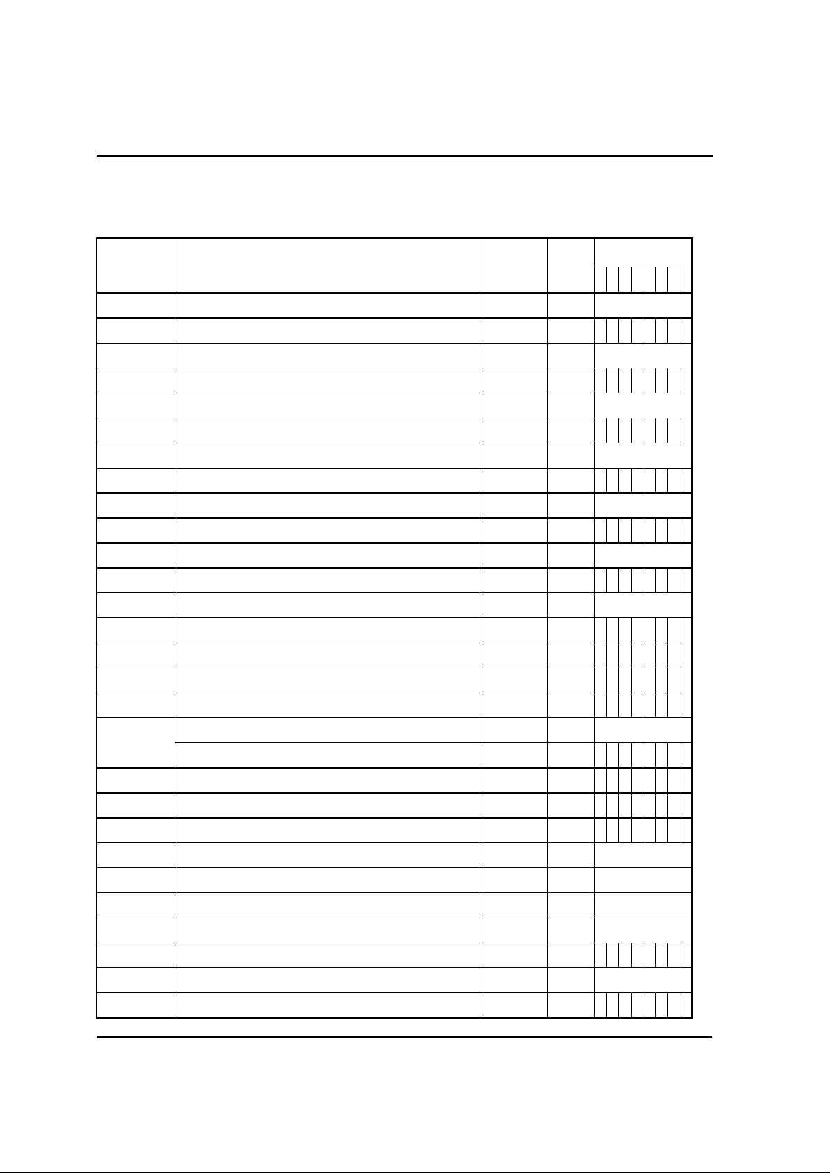
2.2.4. Peripheral Register List
Address Register Name
SYMBOL R/W
RESET VALUE
76543210
00C0
H
R0 PORT DATA REGISTER
R0
R/W Undefined
00C1
H
R0 PORT I/O DIRECTION REGISTER
R0DD
W 00000000
00C2
H
R1 PORT DATA REGISTER
R0
R/W Undefined
00C3
H
R1 PORT I/O DIRECTION REGISTER
R0DD
W 00000000
00C4
H
R2 PORT DATA REGISTER
R0
R/W Undefined
00C5
H
R2 PORT I/O DIRECTION REGISTER
R0DD
W 00000000
00C6
H
R3 PORT DATA REGISTER
R0
R/W Undefined
00C7
H
R3 PORT I/O DIRECTION REGISTER
R0DD
W 00000000
00C8
H
R4 PORT DATA REGISTER
R4
R/W Undefined
00C9
H
R4 PORT I/O DIRECTION REGISTER
R4DD
W 00000000
00CA
H
R5 PORT DATA REGISTER
R5
R/W Undefined
00CB
H
R5 PORT I/O DIRECTION REGISTER
R5DD
W 00000000
00CC
H
R6 PORT DATA REGISTER
R6
R/W Undefined
00CD
H
R6 PORT I/O DIRECTION REGISTER
R6DD
W0000----
00D0
H
PORT R4 MODE REGISTER
PMR4
W 00000000
00D1
H
PORT R5 MODE REGISTER
PMR5
W--00----
00D2
H
TEST MODE REGISTER
TMR
W -----000
00D3
H
BASIC INTERVAL REGISTER
BITR
R Undefined
CLOCK CONTROL REGISTER
CKCTLR
W --010111
00E0
H
WATCH DOG TIMER
WDTR
W -0111111
00E2
H
TIMER MODE REGISTER 0
TM0
R/W00000000
00E3
H
TIMER MODE REGISTER 2
TM2
R/W00000000
00E4
H
TIMER0 DATA REGISTER
TDR0
R/W Undefined
00E5
H
TIMER1 DATA REGISTER
TDR1
R/W Undefined
00E6
H
TIMER2 DATA REGISTER
TDR2
R/W Undefined
00E7
H
TIMER3 DATA REGISTER
TDR3
R/W Undefined
00E8
H
A/D CONVERTER MODE REGISTER
ADCM
R/W --000001
00E9
H
A/D CONVERTER DATA REGISTER
ADR
R Undefined
00EA
H
SERIAL I/O MODE REGISTER
SIOM
R/W -0000001
Page 20
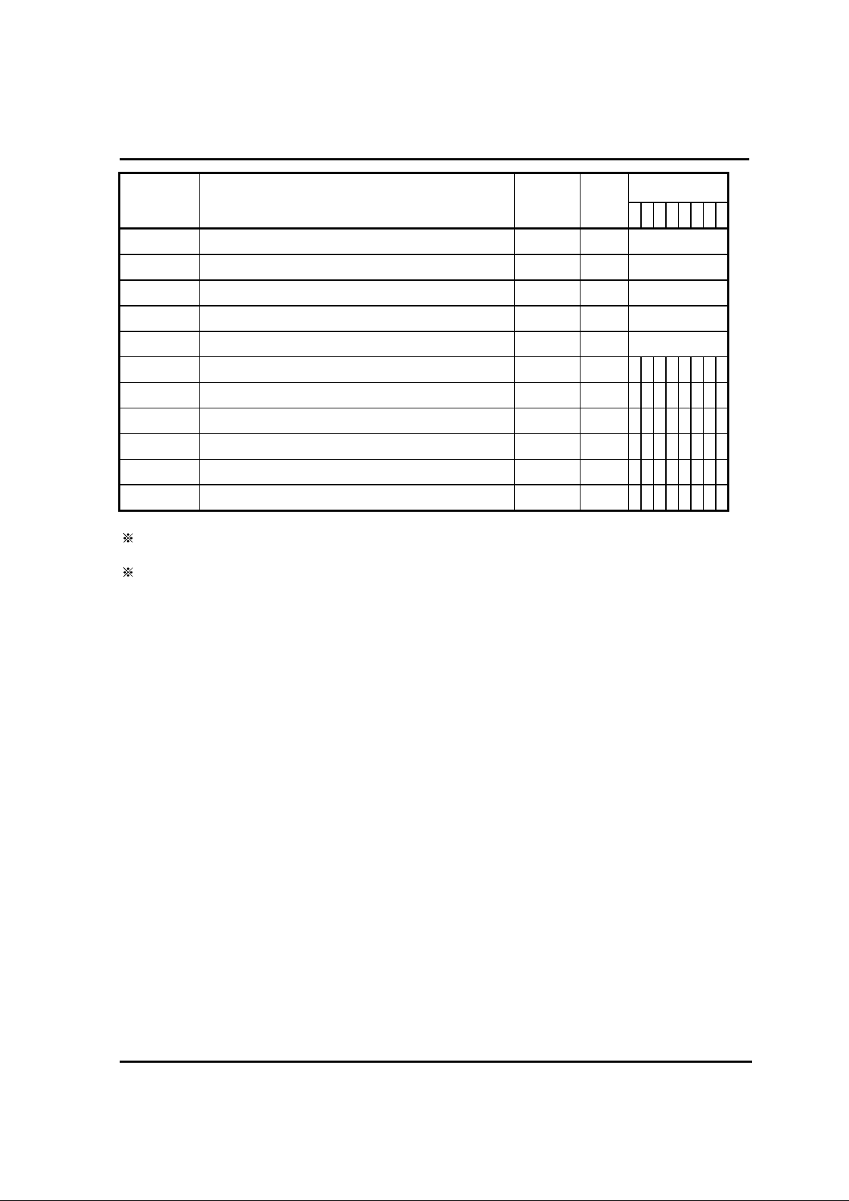
GMS81508/16
15
Address Register Name
SYMBOL R/W
RESET VALUE
76543210
00EB
H
SERIAL I/O REGISTER
SIOR
R/W Undefined
00EC
H
BUZZER DRIVER REGISTER
BUR
W Undefined
00F0
H
PWM0 DATA REGISTER
PWMR0
W Undefined
00F1
H
PWM1 DATA REGISTER
PWMR1
W Undefined
00F2
H
PWM CONTROL REGISTER
PWMCR
W00
00F3
H
INTERRUPT MODE REGISTER
IMOD
R/W --000000
00F4
H
INTERRUPT ENABLE REGISTER LOW
IENL
R/W 0000----
00F5
H
INTERRUPT REQUEST FLAG REGISTER LOW
IRQL
R/W 0000----
00F6
H
INTERRUPT ENABLE REGISTER HIGH
IENH
R/W00000000
00F7
H
INTERRUPT REQUEST FLAG REGISTER HIGH
IRQH
R/W00000000
00F8
H
EXT. INTERRUPT EDGE SELECTION REGISTER
IEDS
W 00000000
-: Not Used
Write Only Register can not be accessed by bit manipulation instruction.
Page 21
HYUNDAI MicroElectronics
16
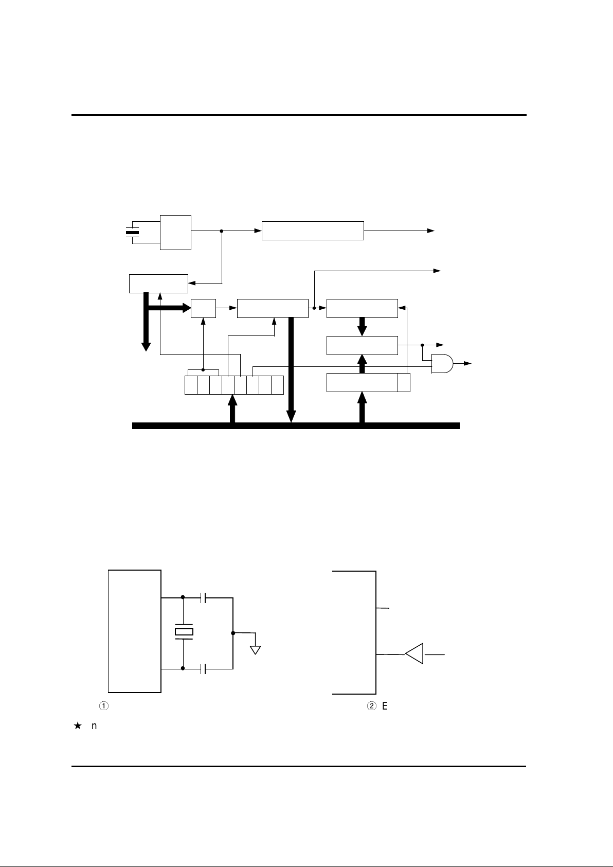
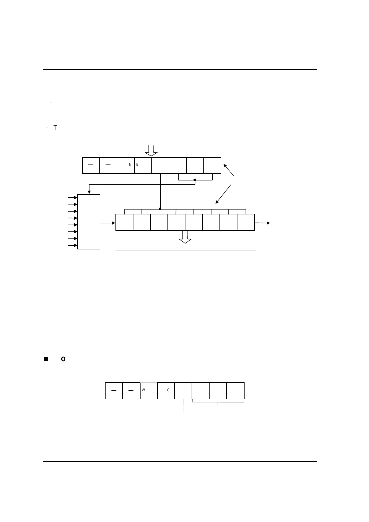
2.3. CLOCK GENERATION CIRCUIT
The clock generation circuit of GM S 81508/16 c onsists of oscillation circuit, prescaler , Basic Interval
Timer.
The source clock of peripherals is provided by 11-bit prescaler.
OSC
Circuit
Clock Pulse Generator
Prescaler
MUX B.I.T.(8) W.D.T.(6)
Comparator
WDTR
0 1 2 3 4 5 6 7
Internal System Clock
IFBIT
IFWDT
BTCL
ENPCK
WDTCL
To RESET
Circuit
Internal Data Bus
8
6
6
CKCTLR
6
2.3.1. Oscillation Circuit
The clock signal incoming from crystal osc illator or c er am ic r esonator via Xin and Xout or from
external clock via Xin is supplied to Clock Pulse Generator and P r escaler.
The internal system clock for CPU is made by Clock Pulse Generator, and several peripheral clock
is divided by prescaler.
The clock generation circuit of c ry stal oscillator or ceramic resonator is shown in below.
Crystal Oscillator or Ceramic Resonator External clock
In STOP Mode, The oscillation is stopped,
Xin pin goes to "L" level status, and Xout pin goes to "H" level state.
Xin
Cin
GND
Cout
Xout
Xin
External
Clock
Open
Xout
Page 22
GMS81508/16
17
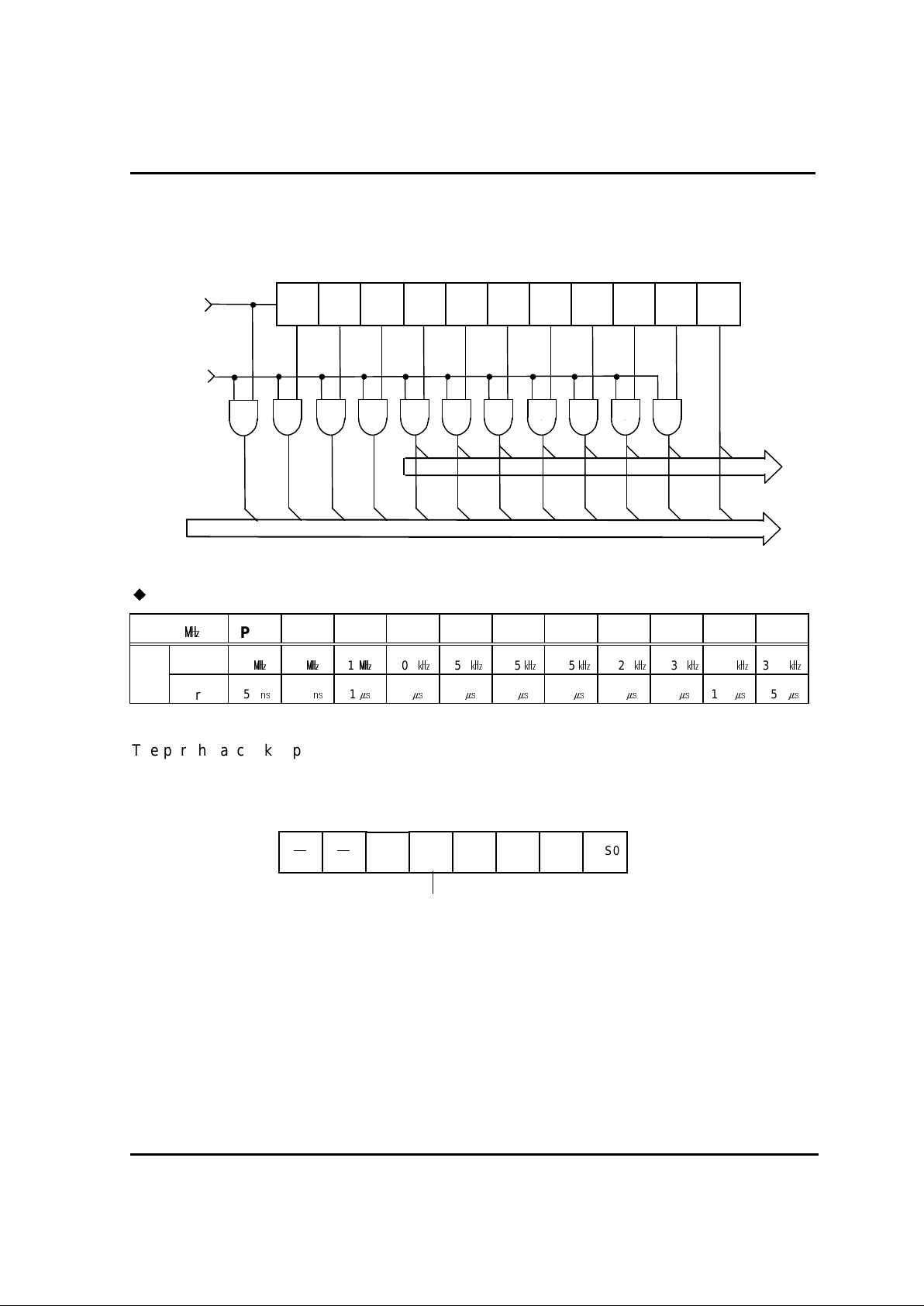
2.3.2. Prescaler
The prescaler consists of 11-bit bi nar y count er , and input clock is supplied by oscillation circuit. The
frequency div i ded by pr escaler is used as a source clock for peripherals.
Frequency- Divided Outputs of Prescal er
f
ex
()
PS1 PS2 PS3 PS4 PS5 PS6 PS7 PS8 PS9 PS10 PS11
Interval
4
2
1
500
250
12562.531.2515.367.183.59
Period
250
500
1
2
4
8
16
32
64
128
256
The peripheral cl oc k suppli ed from prescaler can be stopped by ENPCK. ( Howev er , PS 11 c annot
be stopped by ENPCK)
WWWWWW
76543210
8
Internal Data Bus
Peripherals
ENPCK
f
ex
B.I.T.
PS1 PS2 PS3 PS4 PS5 PS6 PS7 PS8 PS9 PS10 PS11
PS1 PS2 PS3 PS4 PS5 PS6 PS7 PS8 PS9 PS10
PS11
8
PS0
Enable Peripheral Clock
0 : stop
1 : supply
ENPCK
WDTON
BTCL BTS2 BTS1 BTS0
CKCTLR
<00D3H>
Page 23
HYUNDAI MicroElectronics
18
2.4. BASIC INTERVAL TIMER
The Basic Interval Timer(B .I.T.) has 8-bit binar y c ounter . The operations is shown below.
. Generates reference time interval interr upt request as a timer.
. The counting value of B.I.T. c an be r ead.
( Note; The writing at same address overwrites the CKCTLR.)
. The overflow of B.I.T be used the source c loc k of Watch Dog Timer.
2.4.1. Control of Basic Interval Timer
The Basic Interval Timer is free running timer. When the counting value is changed "0FFH" to
"00H" , The interrupt request flag is generated. The counter can be cleared by setting
BTCL
(Bit 3
of CKCTLR) and the BTCL is auto-cleared after 1 machine cy cle. The initial state (after Reset) of
BTCL is “0”.
The input clock of Basic Interval Timer is selec ted by B TS 2~BTS 0 ( Bit2~0 of CKCTLR) among the
prescaler outputs (PS4~PS 11).
The Basic Interval Timer Register (B ITR) c an be read.
The CKCTLR and the BITR have a same address (00D3H). So, If y ou wr ite to this addr es s, the
CKCTLR would be controlled. If you read this address, the c ounting value of B ITR would be read.
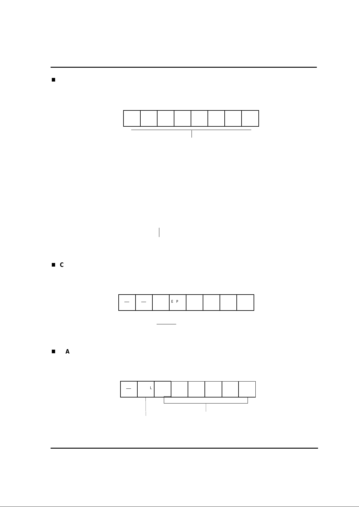
CLOCK CONTROL REGISTER
PS4
WDTON ENPCK
BTCL BTS2 BTS1 BTS0
CKCTLR
bit7 bit6
bit5 bit4
bit3 bit2 bit1 bit0
BITR
PS5
PS6
PS7
PS8
PS9
PS10
PS11
MUX
IFBIT
Internal Data Bus
Internal Data Bus
Same address
when read, it can be read as
counter value. When write, it can
be write as control register.
B.I.T. input clock selection
B.I.T. CLEAR ( When writing )
0 : B.I.T. Free-run
1 : B.I.T. Clear ( auto cleared after 1 machine cycle )
7
6
5 4
ENPCKWDTON
3
BTCL
2
BTS21BTS10BTS0
W W W W W W
<00D3H>
CKCTLR
Page 24
GMS81508/16
19
BASIC INTERVAL TIM E R DATA REGISTER
2.5. WATCH DOG TIMER
The Watch Dog Timer is a means of recover y from a system problem.
In this Device, the Watch Dog Timer consists of 6-bit binary count er , 6-bit comparator and watch
dog timer regi ster (WDTR). The source clock of WDT is overflow of Basi c Interval Timer. The
interrupt request of WDT is generated when the counting value of WDT equal to the contents of
WDTR( bit0~5). T his can be used as s/w int er r upt or MICOM RESET signal(Watch Dog Function).
2.5.1. Control of Watch Dog Timer
It can be used as 6-bit timer or WDT according to bit5(WDTON) of Clock Control Register
(CKCTLR). The counter can be cleared by setting WDTC L ( Bit 6 of WDTR) and the WDTCL is
auto-cleared after 1 machine cycle. The initi al state (after Reset) of WDTCL is “0”.
CLOCK CONTROL REGISTER
WATCH DOG TIMER REGISTER
WDT ON
0 : 6-bit Timer
1 : Watch Dog Timer
7
6
5 4
ENPCK
WDTON
3
BTCL2BTS21BTS10BTS0
W W W W W W
<00D3H>
CKCTLR
Watch Dog Timer Clear
0 : free run
1 : W.D.T counter clear
7
6
WDTCL
5
WDTR5
4 3 2 1 0
W W W
W W W W W
<00E0H>
WDTR
Determines the interval of W.D.T Interrupt
WDTR3WDTR4 WDTR0WDTR1WDTR2
B.I.T data
7
6
5 4
3
2
1
0
R
R
R R R R R R
<00D3H>
BITR
Page 25
HYUNDAI MicroElectronics
20
The interval of WDT interr upt is decided by the interrupt interval of Basic Interval Timer and the
contents of WDTR.
The interval of WDT = The contents of WDTR The interval of B.I.T.
Caution) Do not use the contents of WDTR = "0"
The relationship between the input clock of B.I.T and the output of W.D.T. (@8MHz)
BTS2BTS1BTS0 B.I.T. Input Clock The cycle of B .I.T. The cycle of W.D.T.(max)
000
PS4 ( 2 ) 512
32,256
001
PS5 ( 4 ) 1,024
64,512
010
PS6 ( 8 ) 2,048
129,024
011
PS7 ( 16 ) 4,096
258,048
100
PS8 ( 32 ) 8,192
516,096
101
PS9 ( 64 ) 16,384
1,032,192
110
PS10 ( 128 ) 32,768
2,064,384
111
PS11 ( 256 ) 65,536
4,128,768
2.5.2. The output of WDT signal
The overflow of WDT can be output through R54/WDT O port by setting bit4 of P M R5( WDTS ) to
"1".
PORT R5 MODE REGISTER
<00D1H>
PMR5
7
-
6
-5BUZS
4
WDTS
3
-
2
-
1
-
0
-
WW
R54/WDT O Selection
0 : R54 ( Input / Output )
1 : WDTO ( Output )
Page 26
GMS81508/16
21
2.6. TIMER
The GMS81508/16 has four multi-functional 8-bit bi nar y timers(Timer0~Timer 3).
Timer0 (or Timer2) is can be used as a 16-bit timer/event counter wit h Timer 1(or Timer3). The
Timer0-1 and Tim er 2- 3 hav e same f uncti ons and structures. So, We will explains about Timer0 and
Timer1 only.
Operation Mode of Timer
Timer0,Timer2 Timer1,Timer3
-. 8-bit Interval Timer
-. 8-bit Event Counter
-. 8-bit input capture
-. 8-bit Interval Timer
-. 8-bit rectangular pulse
output
-. 16-bit Interval Timer
-. 16-bit Event Counter
-. 8-bit r ectangular pulse output
ck
PS6
T0CN
T1ST
INT0
CAP0
T0ST
PS6
2
TDR0
16bit Mode
16bit Mode
MUX
8
TM0
7
1 03 25 47 6
TDR1
IFT0
INTR0
T1O
IFT1
8
8
Comparator 0
8
Comparator 1
Data Reg. 1Data Reg. 0
8
T 0
8
T 1
8 8
Clea
ck
Clea
1
MUX
0
0
MUX
1
F / F
EDGE
1
MUX
0
MUX
2
Page 27
HYUNDAI MicroElectronics
22
TIMER MODE REGISTER 0,2(TM0,TM2)
TIMER DATA REGISTER(TDR0 ~ TDR3)
T1 Input Clock Selection
00 : Connection to T0 (16bit Mode )
01 : PS2 ( 500)
10 : PS4 ( 2)
11 : PS6 ( 8)
T3 Input Clock Selection
00 : Connection to T2 (16bit Mode )
01 : PS2 ( 500)
10 : PS4 ( 2)
11 : PS6 ( 8)
T0 Input Clock Selection
00 : EC0
01 : PS2 ( 500)
10 : PS4 ( 2)
11 : PS6 ( 8)
T2 Input Clock Selection
00 : EC2
01 : PS2 ( 500)
10 : PS4 ( 2)
11 : PS6 ( 8)
<00E2H>
<00E3H>
TM0
TM2
7
7
CAP0
CAP2
6
6
T1ST
T3ST
5
5
T1SL1
T3SL1
4
4
T1SL0
T3SL0
3
3
T0ST
T2ST
2
2
T0CN
T2CN
1
1
T0SL1
T2SL1
0
0
T0SL0
T2SL0
R/W
R/W
R/W
R/W
R/W
R/W
R/W
R/W
R/W
R/W
R/W
R/W
R/W
R/W
R/W
R/W
T0 Start/Stop control
0 : Count Stop
1 : Counting start after clearing T0
T2 Start/Stop control
0 : Count Stop
1 : Counting start after clearing T2
T0 Start/Stop control
0 : COUNT Stop
1 : COUNT Start
T2 Start/Stop control
0 : COUNT Stop
1 : COUNT Start
Input Capture Selection
0 : Timer/Counter
1 : Input Capture
Input Capture Selection
0 : Timer/Counter
1 : Input Capture
T1 Start/Stop control
0 : Cout Stop
1 : Counting start after clearing T1
T3 Start/Stop control
0 : Cout Stop
1 : Counting start after clearing T3
TDR0~3
7 6 5 4 3 2 1 0
R/W R/W R/W R/W R/W R/W R/W R/W
( WRITE)
Modulo Data Write
( READ )
Count Value Read
<00E4H~00E7H >
Page 28
GMS81508/16
23
2.6.1. Control of Timer
T0 ( T1 ) consists of 8-bit Binary Up-Counter. When the counting value of Timer0 , Timer1 and
Timer0-1(16bit) become equal to the contents of Timer Data Register(TDR0,TDR1,TDR0-1) v alue,
the counter is cl ear ed to "00H" and restarts count-up operati on. At this time, Interrupt request ( IFT0
or IFT1) is generated.
Any of the PS2, PS4, PS6 or external clock can be selected as the clock source of T0 by
bit1(T0SLI) and bit0(T0SL0) of TM0. Any of the PS 2, PS4, PS6 or ov erflow of T0 can be selected
as the clock source of T1 by bit5( T1SL1) and bit4(T1SL0) of TM0. When the overflow of T0 is
selected as input cl oc k of T1, Timer 0-1 operates as 16 -bit timer. In thi s case, Timer0-1 only is
controlled by T0ST,T0CN and the interrupt vector is Timer0 vector.
The operation of T0, T1 is cont r olled by bit3(T0ST), bit2(T 0CN) and bi t6(T1ST) of TM0. T0CN
controls count stop/start without cleari ng c ounter. T0ST and T1ST control count stop/star t after
timer clear. In order to enable count-up of timer , T0CN, T0ST and T1ST should become “1”. In
order to start c ount-up after clearing of counter, T 0ST or T1ST shoul d be set to "1" after set to "0"
temporarily .
Interval Period
InterruptInterruptInterrupt
MATCHMATCHMATCH
ClearClearClear
00
H
IFT0
T0 VALUE
TDR0 VALUE
Count
Count
StopCountStop
“0” “1” Start
“0” “1” Clear & Start
InterruptInterrupt
MATCHMATCH
ClearClearClear
00
H
IFT0
T0 VALUE
TDR0 VALUE
T0ST
COUNTER
T0CN
Page 29

HYUNDAI MicroElectronics
24
By read Timer Data Register(TDR0~3),The counting value of timer can be read at any time.
2.6.2. Interval Timer
The interrupt cycle is determined by the source c lock of timer and the contents of TDR.
Interrupt cycle = source clock the contents of TDR
In order to write data to TDR, you have to stop timer. otherwise, TDR value is invalid.
Maximum Interrupt Cycle according to source clock @ fex=8MHz
8-bit TIMER Mode 16-bit TIMER M ode
source clock max. c ount sour c e c loc k max . count
PS2 ( 0.5
) 128
PS2 ( 0.5 ) 32,768
T0,T2
PS4 ( 2 ) 512
PS4 ( 2 ) 131,072
PS6 ( 8 ) 2,048
PS6 ( 8 ) 524,288
PS2 ( 0.5 ) 128
T1,T3
PS4 ( 2 ) 512
PS6 ( 8 ) 2,048
2.6.3. Event Counter
The event counter operates in the same way as the interval timer except it counts the external
event input from R44/EC0 and R45/EC1 port. it only counts at the falling edge of event input clock.
In order to input of external event clock, the relevant Port Mode Register(bit4,bit5 of PMR4) is set
to "1". TDR value should be initialized to “FFH” because timer is cleared when it equals to TDR
value, but if you want to use inter r upt, TDR value should be written to "1H~FFH".
2.6.4. Pulse Output
A pulse width 50% cycle duty is output to the R46/T1 O or R47/T3 O por t and rever se the output
when timer interrupt is generated. This c r eates a pulse per iod whic h is two times that of the timer
interrupt cycle. The output pulse period is determined by the source clock of timer and the contents
of TDR.
output period = source clock() the contents of TDR 2
In order to output of pulse, the bit6,bit7 of PMR4 is set to "1".
2.6.5. Input Capture
This function measures the period or width of pulse input from external INT. ( R40/INT0, R42/INT2)
port. The period of pulse is measured by selec ting rising edge or falling edge of the interrupt edge
select register(IEDS ) and the width of pulse is measured by selecting both edge of IEDS.
The external interrupt is generated at the valid edge acc or ding to IEDS . At this time, The c ounting
value of timer is loaded into TDR and counter is cleared and restarts count-up.
Page 30

GMS81508/16
25
R40/INT0
or
R42/INT2
Rising Edge
Falling Edge
Both Edge
Period
“H”Width “L”Width
Timer Operation
the counting value of timer is latched
timer is cleared to 00H
timer restart count-up
PORT R4 MODE REGISTER
<00D0H>
PMR4
7
T3S6T1S
5
EC2S
4
EC0S
3
INT3S
2
INT2S
1
INT1S
0
INT0S
W
W
W
WW
W W W
R44/ EC0 Sele c tion
0 : R44 ( Input / Output )
1 : EC0 ( Input )
R45/ EC2 Sele c tion
0 : R45 ( Input / Output )
1 : EC2 ( Input )
R47 / T3 Selection
0 : R47 ( Input / Output )
1 : T3 ( Output )
R46 / T1 Selection
0 : R46 ( Input / Output )
1 : T1 ( Output )
R40 / INT0 Selection
0 : R40 ( Input / Output )
1 : INT0 ( Input )
R42 / INT2 Selection
0 : R42 ( Input / Output )
1 : INT2 ( Input )
Page 31

HYUNDAI MicroElectronics
26
2.7. EXTERNAL INTERRUPT
An interrupt request is gener ated when a level-c hange from "H" to "L" or "L" to "H" of
INT0,INT1,INT2,INT3 pin is detected. The edge of external interrupt is selected by interrupt edge
selection register(IEDS) and ports( R40,R41,R42,R43) c or r esponding to INT0,INT1,INT4,INT3 ar e
determined as a input port for external inter r upt by bit0~3 of port4 mode register(PM R4).
EXT. INTERRUPT EDGE SELECTION REGISTER
<00D0H>
PMR4
7
T3S6T1S
5
EC2S
4
EC0S
3
INT3S
2
INT2S
1
INT1S0INT0S
W
W
W
WW
W W W
R40 / INT0 Selection
0 : R40 ( Input / Output )
1 : INT0 ( Input )
R43 / INT3 Selection
0 : R43 ( Input / Output )
1 : INT3 ( Input )
R41 / INT1 Selection
0 : R41 ( Input / Output )
1 : INT1 ( Input )
R42 / INT1 Selection
0 : R42 ( Input / Output )
1 : INT2 ( Input )
<00F8H>
IEDS
7
IED3H6IED3L5IED2H4IED2L
3
IED1H2IED1L1IED0H0IED0L
WWWW W
W W
W
INT0 Edge Selection
00 : 01 : Falling
10 : Rising
11 : Falling & Rising
INT1 Edge Selection
00 : 01 : Falling
10 : Rising
11 : Falling & Rising
INT3 Edge Selection
00 : 01 : Falling
10 : Rising
11 : Falling & Rising
INT2 Edge Selection
00 : 01 : Falling
10 : Rising
11 : Falling & Rising
Page 32

GMS81508/16
27
2.8. A/D CONVERTER
A/D Converter has an 8-bit resolution, and input is possible up to 8 channel.
A/D Converter consists of Analog Input Multipl ex er, A/D c onv er t Mode Register, Resistance Ladder,
Sample and Holder, S uccessive Approximation Circ uit and A/D Conversion Data Register.
Ladder
Resistor
Decoder
MUX
S/H
Control Register
Successive
Approximation
Circuit
A/D Conversion
Data Register(8bit)
ADEN ADS2 ADS1 ADS0 ADST ADSF--
AN0
AN1
AN2
AN3
AN4
AN5
AN6
AN7
COMPARATOR
AVref
AVss
Internal Data Bus
IFA
2.8.1. Control of A/D Converter
The analog input is selected by bit2~4 of A/D Converter Mode Register( ADCM). This bits chooses
among AN0~AN7. The ot her anal og pins which ar e not used not A/D conversion be used as
normal port.
The A/D Conversi on is start ed by setting A/D Conversion Start bit (ADST) to "1"(only for ADEN=1).
After A/D Conversion is started, ADST is cleared by hardware. During A/D Conversion, when
ADST is set to "1", A/D Conversi on starts again from the beginni ng.
The analog input vol tage and the reference voltage are c ompared and t he r esul t is stored in the
A/D Converter Data Register(ADR) and ADSF(bit0 of ADCM) is set to "1". The A/D int er r upt
request is generated at the completion of A/D conver si on.
The result of the conversion is obtained by reading out the A/D r egister ( A DR) .
Page 33

HYUNDAI MicroElectronics
28
A/D CONVERTER MODE REGISTER(ADCM)
A/D CONVERTER DATA REGISTER(ADR)
<00E8H>
ADCM
7
6
5 4
ADS2
ADEN
3
ADS12ADS01ADST0ADSF
- - R/W R/W R/W R/W R/W R/W
A/D Conversion Status bit
0 : during A/D Conversion
1 : completed A/D Conversion
A/D Converter input select
000 : channel 0(AN0)
001 : channel 1(AN1)
010 : channel 2(AN2)
011 : channel 3(AN3)
100 : channel 4(AN4)
101 : channel 5(AN5)
110 : channel 6(AN6)
111 : channel 7(AN7)
A/D Converter Enable bit
0 :Disable A/D Converter
1 : Enable A/D Converter
A/D Conversion Start bit
0 : invalid
1 : Start A/D Conversion
(after 1 cycle, be cleared to "0")
<00E8H>
ADCM
7
6
5 4
ADS2
ADEN
3
ADS12ADS01ADST0ADSF
- - R/W R/W R/W R/W R/W R
A/D Conversion Status bit
0 : during A/D Conversion
1 : completed A/D Conversion
A/D Converter input select
000 : channel 0(AN0)
001 : channel 1(AN1)
010 : channel 2(AN2)
011 : channel 3(AN3)
100 : channel 4(AN4)
101 : channel 5(AN5)
110 : channel 6(AN6)
111 : channel 7(AN7)
A/D Converter Enable bit
0 :Disable A/D Converter
1 : Enable A/D Converter
A/D Conversion Start bit
0 : invalid
1 : Start A/D Conversion
(after 1 cycle, be cleared to "0")
<00E9H>
ADR
7
6
5 4
3
2
1
0
R R
R R R R R R
A/D Conversion Data
Page 34

GMS81508/16
29
2.9. SERIAL I/O
The serial I/O is 8-bit cl oc k synchronous type and consists of serial I/ O r egister, serial I/O mode
register, cl oc k sel ection circuit octal counter and control circuit.
SIOR
1 03 25 47 6
Sclk
Octal Counter
Control
Circuit
Internal Data BUS
Internal Data BUS
SM0
SM1
Srdy
Srdy0
Srdy In
2
MUX
PS5
PS4
PS3
IFSIO
Exclk
R
Q
S
Sin
Sout
67 0
SIOM
SM0 SOSFSIOSTSCK0SCK1
Srdy SM1
Page 35

HYUNDAI MicroElectronics
30
Serial I/O Mode Register
This register controls serial I/O function. According to SCK 1 and S CK 0, the internal clock or
external clock can be selected.
Serial I/O Data Register
The Serial I/O Data Register (SIOR) is a 8-bit shift register. First LSB is send or is received.
<00EBH>
SIOR
7
D76D65D54D43D32D21 D10D0
R/W R/W R/W R/W R/W R/W R/W R/W
At transmittion
Sending Data at Sending Mode
Receiving Data at Receiving Mode
<00EAH>
SIOM
7
6
Srdy5SM14SM03SCK12SCK01SIOST0SIOSF
R/W R/W R/W R/W R/W R/W R
Serial Transmission Clock Selection
00 : PS3 ( 1
)
01 : PS4 ( 2 )
10 : PS5 ( 4 )
11 : External Clock
Serial Operation Mode
00 : Normal Port(R52,R51,R50)
01 : Sending Mode(Sclk,Sout,R50)
10 : Receiving Mode(Sclk,R51,Sin)
11 : Sending & Receiving
Md(SlkS Si)
Serial Transmission Start
0 : Invalid
1 : Start(After one SCK, becomes”0”)
Serial Transmission Status Flag
0 : during transmission
1 : finished
R53/Srdy Selection
0 : R53
1 : Srdy
Page 36

GMS81508/16
31
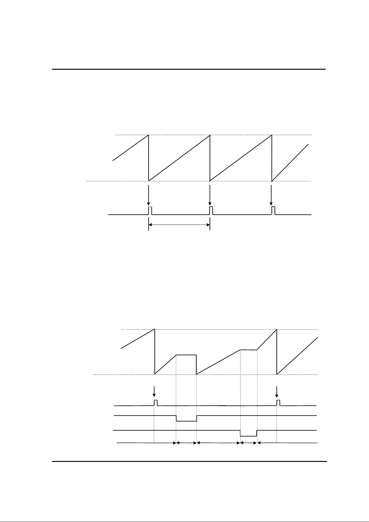
2.9.1. Data Transmission/Receiving Timing
The serial transmission is started by setting SIOST( bit1 SIOM) to ”1”. After one cycle of SCK,
SIOST is cleared autom atically to “0”. The serial output data from 8-bit shift register is output at
falling edge of Sclk. and input data is latched at rising edge of S cl k . When transmission clock is
counted 8 times, seri al I/ O counter is cleared as “0”. Transmission clock is halted in “H” state
and serial I/O i nterr upt (IFSIO) occurred.
Timing Diagram of Seri al I/O
2.9.2. The Serial I/O operation by Srdy pin
tr ansmission clock = external cl ock
The Srdy pin becomes "L" by SIOST = "1". This signal tells to the external system that this device
is ready for seri al transmission. The external system detects the "L" signal and starts transmission.
The Srdy pin becomes "H" at the fi r st ri si ng edge of transmission clock.
tr ansmission clock = internal cl oc k
The I/O of Srdy pin is input m ode. W hen the external system is ready to for serial tr ansmission, the
"L" level is inputt ed at t hi s pi n. At t his time this device starts serial transmission.
SIOST
Srdy(Output)
SIOST
Srdy(Input)
D7D6D5D1 D4D3D2D0
D7D6D5
D1 D4D3
D2
D0
Input Clock
Sclk
Latch
Output
IFSIO
Sin
Sout
SIOST
Page 37

HYUNDAI MicroElectronics
32
2.9.3. The method of Serial I/O
Select transmission/receiving mode
<Notice> When external clock is used, the frequency should be less than 1M Hz and
recommended duty is 50%.
In case of sending mode, write data to be send to SIOR.
Set SIOST to “1” to start serial tr ansm ission.
<Notice > If both transmission mode is selected and transm ission is per formed simultaneously
it would be made error.
The SIO interrupt is generated at the completion of SIO and SIOSF is set to “1”. In SIO
interrupt service routine, correct transmission should be tested.
In case of receiving mode, the r ec eived data is acquired by r eading the S IOR.
2.9.4. The Method to Test Correct Transmission with S/W
Serial I/O Interrupt
Service Routine
SIOSF
SE=0
Write SIOM
Normal Operation Overrun Error
SR
Abnormal
0
0
1
1
Serial Method to Test Tr ansmission.
Note) SE:
Interrupt Enable Regist Low
IENL ( Bit3 )
SR :
Interrupt Request Flag Regist Low
IRQL ( Bit3 )
Page 38

GMS81508/16
33
2.10. PWM
PWM(Pulse Width Modulation) has a 8-bit resolution and the PS8,PS9,PS10,PS 11 of the prescaler
can be selected as input clock PWM.
PWMR0
Comparator
Counter
PWMR1
Comparator
Counter
P1CK1 P1CK0 P0CK1 P0CK0 EN1 EN0 POL1 POL0
S
Q
R
S
Q
R
MUX
MUX
Polarity
Polarity
PS8
PS9
PS10
PS11
PS8
PS9
PS10
PS11
Internal Data Bus
Internal Data Bus
Overflow
Overflow
PWM0
PWM1
PWMCR
2.10.1. Controls of PWM
The input clock is selected by PWM Control Register ( P WMCR) , and the width of pulse is
determined by the PWM Register (PWMR).
The pulse period according to input clock are as follows.
Input clock PWM Period
PS8 (32)8,192
PS9 (64) 16,384
PS10 (128) 32,768
PS11 (256) 65,536
Bit2 (EN0) and bit3 (EN1) of PWM control Register (PWMCR) determine the operation c hannel of
PWM. When EN0=0 and EN1=0, PWM does not executed. The EN0 and EN1 ar e E nable bit of
PWM channel 0 and channel 1 respectively. When EN0=1, PWM channel0 executes. When EN1=1,
PWM channel1 executes.
POLO and POL1 are a polarity control bit of channel0 and channel1. When they are 0, LOW
active. When 1, HIGH active. PWMCR becomes "00h" in reset state.
Page 39

HYUNDAI MicroElectronics
34
PWM CONTROL REGISTER
PWM DATA REGISTER
(a) Active Low
period
(b) Active High
period
pulse width
pulse width
Counter Load Value + 1
Duty Cycle =
100[%]
256
<00F2H>
PWMCR
7
PICK16PICK0
5
P0CK
1
4
P0CK
0
3
EN12EN01POL10POL0
W W W W W W W W
PWM Enable Flag
00 : Disable
01 : PWM0
10 : PWM1
11 : PWM0,PWM1
PWM1 Clock Selection
00 : PS8
01 : PS9
10 : PS10
11 : PS11
PWM0 Clock Selection
00 : PS8
01 : PS9
10 : PS10
11 : PS11
PWM0 Output Polarity
0 : Active Low
1 : Active High
PWM1 Output Polarity
0 : Active Low
1 : Active High
<00F0H>
<00F1H>
PWMR0
PWMR1
7
6
5
4
3
2
1
0
W W W W W W W W
PWM DATA
Page 40

GMS81508/16
35
2.11. BUZZER DRIVER
Buzzer driver c onsi st of 6 bit binary counter, Buzzer Register ( B UR) , and sel ec tor of clock. The wide
range frequency(500Hz~250KHz) can be generated usi ng pr ogr ammable counter. PORT R55 is
assigned for output por t of Buzz er Driver by setting bit5 of PMR5($00D1H) to "1".
BUCK1 BUCK0 BU5 BU4 BU3 BU2 BU1 BU0
MUX
0 1 2 3 4 5 T Q
PS4
PS5
PS6
PS7
6
Buzzer
Output
6bit Counter
WtBUR
Internal Data Bus
PORT R5 MODE REGISTER
BUZZER DATA REGISTER
<00D1H>
PMR5
7
-
6
-
5
BUZ
4
WDTO
3
-
2
-
1
-
0
-
W
W
R55 / BUZ Selec tion
0 : R55 ( Input / Output )
1 : BUZ ( Output )
<00ECH>
BUR
7
BUCK16BUCK0
5
BU54BU43BU32BU21BU10BU0
W W WWWWW
W
Buzzer Count Da ta
Buzzer Source Clo ck
Selection
00 : PS4
01 : PS5
10 : PS6
11 : P
S
7
Page 41

HYUNDAI MicroElectronics
36
2.11.1. Buzzer Driver Operation
The bit0-5 of Buzzer Register (BUR) determines output frequency for buzzer driving. The frequency
is calculated as shown bellows.
N = BUR data
freq. = 1/(source clock ✕ N ✕ 2)
The bit6 and bit7 of Buzzer register (B UR) selects the source clock of the buzzer counter among
PS4 (2us), PS5 (4us), PS6 (8us) and PS7 ( 16us) .
The buzzer counter is cleared by Wt signal of BUR and starts the counting. also, It is cleared by
counter overflow, and continues count-up to output the rectangular wave of duty 50%.
* Caution: don't use BUR register as 00H. (c ounter reset state)
The output frequency of buzzer according to Buzz er Register bit5 - bit0 (fex = 8 MHz)
REG. REG. OUTPUT FREQUENCY[KHz] REG. REG. OUTPUT FREQUENCY[KHz]
LOAD
DEC
LOAD
HEX
PS4
(2us)
PS5
(4us)
PS6
(8us)
PS7
(16us)
LOAD
DEC
LOAD
HEX
PS4
(2us)
PS5
(4us)
PS6
(8us)
PS7
(16us)
1
2
3
4
5
6
7
8
9
10
11
12
13
14
15
16
17
18
19
20
21
22
23
24
25
26
27
28
29
30
31
32
01
02
03
04
05
06
07
08
09
0A
0B
0C
0D
0E
0F
10
11
12
13
14
15
16
17
18
19
1A
1B
1C
1D
1E
1F
20
250
125
83.333
62.5
50
41.666
35.714
31.25
27.778
25
22.728
20.834
19.23
17.858
16.666
15.626
14.706
13.888
13.158
12.5
11.904
11.364
10.87
10.416
10
9.616
9.26
8.928
8.62
8.334
8.064
7.812
125
62.5
41.666
31.25
25
20.834
17.858
15.626
13.888
12.5
11.364
10.416
9.616
8.928
8.334
7.812
7.352
6.944
6.579
6.25
5.952
5.682
5.434
5.208
5
4.808
4.630
4.464
4.310
4.166
4.032
3.906
62.5
31.25
20.834
15.626
12.5
10.416
8.928
7.812
6.944
6.25
5.682
5.682
4.808
4.464
4.166
3.906
3.676
3.472
3.288
3.124
2.976
2.840
2.718
2.604
2.5
2.404
2.314
2.232
2.156
2.084
2.016
1.954
31.25
15.626
10.416
7.812
6.25
5.208
4.464
3.906
3.472
3.126
2.84
2.604
2.404
2.232
2.084
1.9541
1.838
1.736
1.644
1.562
1.488
1.420
1.358
1.302
1.250
1.202
1.158
1.116
1.078
1.042
1.008
0.976
33
34
35
36
37
38
39
40
41
42
43
44
45
46
47
48
49
50
51
52
53
54
55
56
57
58
59
60
61
62
63
21
22
23
24
25
26
27
28
29
2A
2B
2C
2D
2E
2F
30
31
32
33
34
35
36
37
38
39
3A
3B
3C
3D
3E
3F
7.576
7.352
7.142
6.944
6.756
6.578
6.41
6.3
6.098
5.952
5.814
5.682
5.556
5.434
5.32
5.208
5.102
5
4.902
4.808
4.716
4.63
4.546
4.464
4.386
4.31
4.238
4.166
4.098
4.032
3.968
3.788
3.676
3.571
3.472
3.378
3.289
3.205
3.125
3.049
2.976
2.907
2.841
2.778
2.717
2.660
2.604
2.551
2.5
2.451
2.404
2.358
2.315
2.273
2.232
2.193
2.155
2.119
2.083
2.049
2.016
1.984
1.894
1.838
1.786
1.736
1.689
1.645
1.602
1.563
1.524
1.488
1.453
1.421
1.389
1.359
1.33
1.302
1.276
1.25
1.225
1.202
1.179
1.157
1.136
1.116
1.096
1.078
1.059
1.042
1.025
1.008
0.992
0.947
0.919
0.893
0.868
0.845
0.822
0.801
0.781
0.762
0.744
0.727
0.710
0.694
0.679
0.665
0.651
0.638
0.625
0.613
0.601
0.590
0.579
0.568
0.558
0.548
0.539
0.530
0.521
0.512
0.504
0.496
Page 42

GMS81508/16
37
2.12. INTERRUPTS
The interrupt s are usually used when the processing routi ne has the higher priority than on-going
program and a routine muse be executed at specific interval.
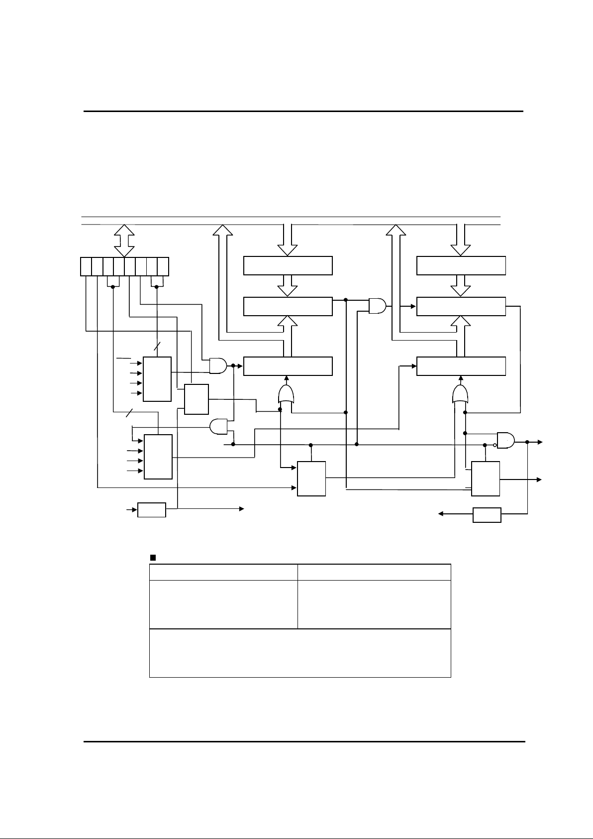
2.12.1. Interrupt Circuit Configuration and Kinds
GMS81508/16 Interrupt circuits consists of I nterrupt Enable Register (IENH, IENL) , Interrupt
Request Register ( IRQH,IRQL), priority cir c uit and selec ting circuit.
The configurat ion of Interrupt circuit is shown in bel ow.
12
IRQL
IRQH
4
7
7
0
RESET
IFT3
D
ata BUS
IMOD
6
I-FLAG
BRK
to C PU
Standby
Mode
Release
PRIORITY
CONTROL
T2R
T3R
IENH
8
10 32 54 76
8
4
10 32 54
T0R
T1R
INT2R
INT3R
INT0R
INT1R
BITR
WDTR
SR
AR
IENL
4
-
5 47 6
4
IFT2
IFT1
IFT0
INT3
INT2
INT1
INT0
IFA
IFWDT
IFBIT
IFS
8
INTERRUPT
VECTOR
ADDRESS
GEN.
Page 43

HYUNDAI MicroElectronics
38
Interrupt Source
The interrupts sources are external interrupt source(INT0, INT1,INT2,INT3), peripheral function
source (T0,T1,T2,T3,B.I.T.,W.D.T.,SIO,A/DC) and software interrupt source(BRK).
After reset input(RESET), the program is executed from the address in reset vector table like
general interrupts.
Type Mask Priority Interrupt Request Source VectorHVector
L
Non
Maskable
1 RST Reset Pin FFFFHFFFE
H
2 INT0R Exter nal Interr upt 0 FFFBHFFFA
H
3 INT1R Exter nal Interr upt 1 FFF9HFFF8
H
4 INT2R Exter nal Interr upt 2 FFF7HFFF6
H
H/W 5 INT3R External Interrupt 3 FFF5HFFF4
H
Interrupt 6 T0R Timer 0 FFF3HFFF2
H
7 T1R Timer 1 FFF1HFFF0
H
8 T2R Timer 2 FFEFHFFEE
H
9 T3R Timer 3 FFEDHFFFC
H
10 AR A/D Converter FFEBHFFEA
H
11 WDTR Watch Dog Timer FFE9HFFE8
H
12 BITR Basic Interval Timer FFE7HFFE6
H
13 SR Serial I/O FFE5HFFE4
H
S/W Interrupt Non
Maskable
BRK Break Instruction FFDFH FFDE
H
2.12.2. Interrupt Control
The interrupts is controlled by the interrupt master enable flag I-Flag(3'rd bit of P SW), interrupt
enable register(IENH,IENL), interrupt r equest register(IRQH,IRQL) except RESET and S/W
interrupt.
Interrupt Enable Register ( IENH, IE NL)
This register is composed of interrupt enable flags of each interrupt source, this flags determines
whether an interrupt will be accepted or not. when enable flag is "0", an interr upt corresponding
interrupt source is prohibited.
Page 44

GMS81508/16
39
Interrupt Request Flag Register ( IRQH, IRQL)
Whenever interr upt request is generated, the inter r upt request flag is set. The request fl ag
maintains '1" unti l interrupt is accepted. The acc epted interrupt request flag is automatically cleared
by interrupt process cycle. Interrupt Request Flag Register ( IRQH, IRQL) is Read/ Write Register.
So, it is possible to be c hec k ed and changed by progr am.
2.12.3. Interrupt Priority
When two or more interr upts requests are generated at the same sampling point, the interrupt
having the higher pri or ity is accepted. The interrupt priority is determined by H/W. however,
multiple prior ity processing through software is possible by using interrupt contr ol flags(IENH, IENL,
I-flag) and interrupt mode register(IMOD).
Interru pt M as ki ng Fl ag
0 : Interrupt Disable
1 : Interrupt Enable
<00F6H>
IENH
7
INT0E6INT1E5INT2E4INT3E3T0E2T1E1T2E0T3E
R/W R/W R/W R/W R/W R/W R/W R/W
<00F4H>
IENL
7
AE6WDTE5BITE4SE
3
-
2
-
1
-
0
-
R/W R/W R/W R/W - - - -
Interrupt Request Flag
0 : Disable
1 : Enable
<00F7H>
IRQH
7
INT0R6INT1R5INT2R4INT3R3T0R2T1R
1
T2R
0
T3R
R/W R/W
R/W R/W
R/W R/W
R/W R/W
<00F5H>
IRQL
7
AR6WDTR5BITR4SR
3
-
2
-
1
-
0
-
R/W R/W R/W R/W - - - -
Page 45

HYUNDAI MicroElectronics
40
2.12.4. Interrupt Sequence
When interrupt is accepted, the on- going pr oc ess is stopped and the inter r upt service routine is
executed. After the interrupt service routine is completed it is nec es sar y to r estore everything to the
state before the interrupt occurred.
As soon as an interrupt is accepted, the contents of the program counter and the program status
word are saved in the stack area. At the same time, the contents of the vector address
corresponding to the accepted interrupt, whic h is in the interr upt vector table, enters into the
program counter and inter r upt service routine is executed.
In the interrupt service routine, the corresponding interrupt r equest flag is cleared and interrupt
master enable flag(I-flag) becomes "0", thereby another interrupts are not accepted before I-flag is
set to "1" by program.
In order to execute the interrupt servic e r outine, it is neces sar y to wr ite the jump addr ess( the fir st
address of the interrupt service routine) in vector table corresponding to each interrupt.
Interrupt Accept Timing
The valid timing after executing Interrupt control Flag
I-Flag is valid, after EI, DI executed
IENH, IENL register is valid after next instruction
1 Cycles
012 Cycles
8 Cycles
System Clock
Instruction
Fetch
Interrupt Overhead :
9 21 Cycles
Int.request Sampling
Interrupt Process Step
Interrupt routine
A command before
Interrupt
Page 46

GMS81508/16
41
Interrupt P rocess St ep Timin g
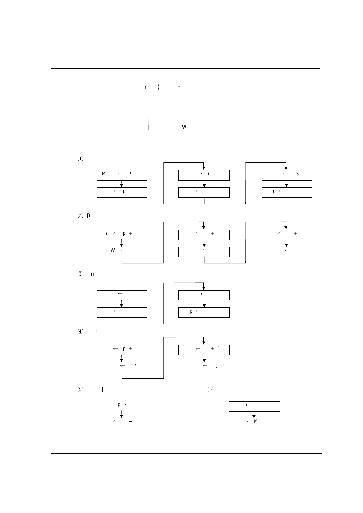
2.12.5. Software Interrupt
The interrupt is the lowest pri or ity order software int er r upt by B RK instruc tion. B-flag is set.
Interrupt vector of BRK instruction is shared with the vector of TCALL 0. Each processing step is
determined by B-Fl ag as a bel ow.
Execution of BRK/ TCALL0
0
BRK or TCALL0
1
TCALL 0 Routine
BRK Interrupt Routine
RET
B-Flag ?
RETI
V.L
System Clock
Instruction
Fetch
sp-2 new pcV.HV.Lsp-1pc sp
Address Bus
PSW OpcodeADHADLPCL
V.L, V.H is Vector Address, ADL, ADH is start Address of Interrupt
Service Routine as Vector Contents
Interru pt Process Step Interrupt Service Routin e
not Used PCH
Data Bus
Internal Read
Interna l Write
Page 47

HYUNDAI MicroElectronics
42
2.12.6. Multiple Interrupt
When an interrupt is accepted, and program flow goes to the interrupt service routine. The inter r upt
master enable flag(I-flag) is automatically cleared and other interrupts are inhibited. When inter r upt
service is completed by RETI instruction, I-flag is set automatic ally . If other inter r upts ar e gener ated
during interrupt service, The interr upt having higher priority is accepted when the previous interrupt
service routine is completed.
In order to multiple interrupts, I-flag must be cleared by EI instruction within the interrupt routine.
Then, The higher priority interrupt is ac c epted among the inter r upts that interrupt request flag is "1".
Interrupt Mode Register ( IMOD)
if IM1,IM0 is selected as a "01", the interrupt selected by IP0~IP3 c an be ac c epted and other
interrupts are not accepted. Using this register, we can c hange the inter r upt priority order by s/w.
Interrupt Mode Definition
00 : Mode 0 (Priority by H/W)
01 : Mode 1(Definition by IP3IP0)
1- : Inhibit Interrupt
Interrupt Definition Selection
0001 : INT0
0010 : INT1
0011 : INT2
0100 : INT3
0101 : TIMER0
0110 : TIMER1
0111 : TIMER2
1000 : TIMER3
1001 : ADC
1010 : WDT
1011 : BIT
1100 : SIO
<00F3H>
IMOD
7
6
5
IM14IM03IP32IP21IP10IP0
R/W R/W R/W R/W R/W R/W
Page 48

GMS81508/16
43
When multipl e interr upt is accepted, it is possible to change I nterrupt Accept Mode.
In case of multiple interrupt at hardware priority ac cept mode(Mode0)
In case of multiple interrupts nest H/W priority acc ept m ode ( M ode0) and S/W selec tion accept
mode(Mode1)
EI
EI
EI
Main Program
( Mode 0 )
1’st INT. Routine
( Mode 0 )
2’nd INT. Routine
( Mode 0 )
3’rd INT. Routine
Interrupt
Interrupt
Interrupt
EI
EI
EI
Main Program
( Mode 0 )
1’st INT. Routine
( Mode 0 )
2’nd INT. Routine
( Mode 1 )
3’rd INT. Routine
Interrupt
Interrupt
Interrupt
Reload IMOD
Stacking IMOD
Change Mode
Page 49

HYUNDAI MicroElectronics
44
2.13. STANDBY FUNCTION
To save the consuming power of device, GMS81508/16 has STOP Mode.
In this mode, the execution of pr ogram is stopped. Stop Mode entered by STOP instruction.
At STOP Mode, Device Operation State.
Peripheral Function STOP Mode
Oscillator
CPU Clock
RAM, Register Retain
I/O Port Retain
Prescaler
Basic Interval Timer
Serial I/O Operation( External Clock Selection)
WDT, Timer, A/DC,PWM,
Buzzer Driver
Address Bus, Data Bus Retain
Rd, Wt, R/W Retain
HALT, BRQ, BAK Active
C"L" level
SYNC "H" level
halt
STOP
IFBIT
CPU Clock
Release Signal from Interrupt Circuit
RESET
Clock Pulse GEN.
MUX
Prescaler
RQ
SQ
Overflow
Detection
Basic Interval Timer
RQ
SQ
OSC.
Circuit
Page 50

GMS81508/16
45
2.13.1. STOP Mode
STOP Mode can be entered by STOP instruc tion during program execution. In STOP mode,
osc illator is stopped to make all clocks stop, which leads to the mode requiring much less power
consumption. Al l r egister and RAM data are preserved.
Caution) NOP instru ct io n h ave to be written more than 2 to next lines of STOP instruction.
2.13.2. STOP Mode Release
The release of STOP mode is done by reset input or interrupt. When t her e is a release signal of
STOP mode, the instruction execution is started aft er stabilization oscillation time set by program.
After releasi ng STOP mode, instruction executi on is different by I-Flag(bit 2 of PSW).
If I-Flag = “1” entered Interr upt Service Routine,
If I-Flag = “0” execute program from next instr uc tion of STOP instruction.
STOP Mode Release
Release
Factor
Release Method
RESET By RESET pin=Low level, and Device is initialized.
INT0,INT1
INT2,INT3
In the state of enable flag=1 corresponding to each int er r upt at
the edge.
Serial I/O When Serial I/O is executed by external clock, STOP mode is
released.
Release Timing of STOP Mode
System Clock
Release Signal
by interrupt
STOP
Stabilization Oscillation TimeSTOP Mode
determi n ed by program.
RESET
Stabilization oscillation time + 8 Cycles
Page 51

HYUNDAI MicroElectronics
46
When release the STOP Mode, to secure oscillation stabilization time, we use Basic Interval Timer.
So, before execution STOP instruction, we must select suitable B.I.T. clock for oscillation
stabilization time. Otherwise, It is possible to release by only RES ET input.
Because STOP mode is released by interr upt, even if both of interrupt enable bit(IE) and interrupt
request flag is "1", STOP mode can not be executed.
STOP Mode Releasing Flow
0
1
NOP
NOP
Interrupt Service Routine
I-Flag ?
0
1
STOP Mode Release
Interrupt Request
IE ?
STOP Mode
STOP Command
Page 52

GMS81508/16
47
2.14. RESET FUNCTION
To reset the device, maintain the RESET="L" at least 8 machine cy cle after power supplying and
oscillation stabilization.
RESET terminal is organized as schmitt input.
If initial value is undefined, it is needed initialize by a S/W.
RESET Operation Timing
Opcode
System Clock
Instru ctio n Fe tch
?
Start
FFFFFFFE
?? ?
Address Bus
FE? ADHADL?
FFFEH, is vector ad dr ess an d ADL, AD H is star t addr ess of m ain pr ogr am
as vector contents
RESET Process Step Main Program
? ?
Data Bus
Internal Read
RESET
Page 53

HYUNDAI MicroElectronics
48
3. I/O PORTS
There are 7-ports(R0~R6) in this device. This ports are double-functional ports and the function can
be selected by program.
The direction of ports is determined by Port Direction Register.(1=output, 0=input) The data that is
written on the programmed output pin is stored in the port data r egister and is transferred to the
output pin. When data is input to the programmed pin. data is read not from output pin but from port
data register. therefore, pr eviously output data can be read correctly regardless or the logic al level
of the pin due to output loading.
Because the programmed input pin is floating, the value of the pin can be read correctly. When
data is written to the programmed input pin, it is written only to the por t data register and the pin
remains floating.
3.1. R0 PORT
R0 Port is composed of 8-bit programmable I/O pin.
Register Name Symbol R/W Address Initial Value
R0 I/O Direction Register R0DD W 00C1
H
0000 0000
R0 PORT Data Register R0 R/W 00C0
H
Not initialized
R0 PORT I/O DIRECTION REGISTER
R0 PORT DATA REGISTER
Determines I/O of R0 port
0 : Input
1 : Output
<00C1H>
R0DD
7
R0DD76R0DD65R0DD54R0DD43R0DD32R0DD21R0DD10R0DD0
W W W W W W W W
Port R0 output data
<00C0H>
R0
7
R076R065R054R043R032R021R010R00
R/W R/W R/W R/W R/W R/W R/W R/W
Page 54

GMS81508/16
49
Pin Function According to Operati on Modes
PIN Single Chip Mode Microprocessor Mode
R00/D0 I/O I/O
R01/D1 I/O I/O
R02/D2 I/O Programmable I/O Port I/O Data I/O Port from/to External Memory
R03/D3 I/O I/O for CPU.
R04/D4 I/O I/O
R05/D5 I/O I/O
R06/D6 I/O I/O
R07/D7 I/O I/O
3.2. R1 PORT
R1 Port is composed of 8- bit progr ammable I/O pin.
Register Name Symbol R/W Address Initial Value
R0 I/O Direction Register R1DD W 00C3
H
0000 0000
R0 PORT Data Register R1 R/W 00C2
H
Not initialized
R1 PORT I/O DIRECTION REGISTER
R1 PORT DATA REGISTER
Pin Function According to Operati on Modes
Determines I/O of R1 port
0 : Input
1 : Output
<00C3H>
R1DD
7
R1DD76R1DD65R1DD54R1DD43R1DD32R1DD21R1DD10R1DD0
W W W W W W W W
Port R1 outp ut d ata
<00C2H>
R1
7
R176R165R154R143R132R121R10R10
R/W R/W R/W R/W R/W R/W R/W R/W
Page 55

HYUNDAI MicroElectronics
50
PIN Single Chip Mode Microprocessor Mode
R10/A0 I/O O
R11/A1 I/O O
R12/A2 I/O Programmable I/O Port O low 8bit address of External Memory
R13/A3 I/O O for CPU.
R14/A4 I/O O
R15/A5 I/O O
R16/A6 I/O O
R17/A7 I/O O
3.3. R2 PORT
R2 Port is composed of 8-bit programmable I/O pin.
Register Name Symbol R/W Address Initial Value
R2 I/O Direction Register R2DD W 00C5
H
0000 0000
R2 PORT Data Register R2 R/W 00C4
H
Not initialized
R2 PORT I/O DIRECTION REGISTER
R2 PORT DATA REGISTER
Determines I/O of R2 port
0 : Input
1 : Output
<00C5H>
R2DD
7
R2DD76R2DD65R2DD54R2DD43R2DD32R2DD21R2DD10R2DD0
W W W W W W W W
Port R2 output data
<00C4H>
R2
7
R276R265R254R243R232R221R210R20
R/W R/W R/W R/W R/W R/W R/W R/W
Page 56

GMS81508/16
51
Pin Function According to Operati on Modes
PIN Single Chip Mode Microprocessor Mode
R20/A8 I/O O
R21/A9 I/O O
R22/A1 0 I/O Programmab l e I/O Por t O up p er 8bit address of External M em ory
R23/A11 I/O O for CPU.
R24/A12 I/O O
R25/A13 I/O O
R26/A14 I/O O
R27/A15 I/O O
3.4. R3 PORT
R3 Port is composed of 8- bit progr ammable I/O pin.
Register Name Symbol R/W Address Initial Value
R3 I/O Direction Register R3DD W 00C7
H
0000 0000
R3 PORT Data Register R3 R/W 00C6
H
Not initialized
R3 PORT I/O DIRECTION REGISTER
R3 PORT DATA REGISTER
Determines I/O of R3 port
0 : Input
1 : Output
<00C7H>
R3DD
7
R3DD76R3DD65R3DD54R3DD43R3DD32R3DD21R3DD10R3DD0
W W W W W W W W
Port R3 outp ut d ata
<00C6H>
R3
7
R376R365R354R343R332R321R310R30
R/W R/W R/W R/W R/W R/W R/W R/W
Page 57

HYUNDAI MicroElectronics
52
Pin Function According to Opera tion Modes
PIN Single Chip Mode Microprocessor Mode
R30 I/O O Rd : external memory read strobe
R31 I/O O Wt : external memory write strobe
R32 I/O Programmable I/O Port O R/W :Read/Write cycle output pin of CPU
R33 I/O O C : timing signal output pin
R34 I/O O SYNC : op code fetch output pin of CPU
R35 I/O O BRK : bus acknowledge output pin of
CPU
R36 I/O I BRQ : bus request input pin of CUP
R37 I/O I HALT : CPU halt input pin
3.5. R4 PORT
R4 Port is composed of 8bit programmable I/O port and this port are double functional pin.
Register Name Symbol R/W Address Initial Value
R4 I/O Direction Register R4DD W 00C9
H
0000 0000
R4 Port Data Register R4 R/W 00C8
H
Not initialized
Port R4 Mode Register PMR4 W 00D0
H
0000 0000
Interrupt Edge Select Register IEDS R/W 00F8
H
0000 0000
R4 PORT I/O DIRECTION REGISTER
R4 PORT DATA REGISTER
Port R4 output data
<00C8H>
R4
7
R476R465R454R443R432R421R410R40
R/W R/W R/W R/W R/W R/W R/W R/W
Determines I/O of R4 port
0 : Input
1 : Output
<00C9H>
R4DD
7
R4DD76R4DD65R4DD54R4DD43R4DD32R4DD21R4DD10R4DD0
W W W W W W W W
Page 58

GMS81508/16
53
PORT R4 MODE REGIST E R
INTERRUPT EDGE SELECTION REGISTER
3.6. R5 PORT
R5 Port is composed of 8- bit progr ammable I/O port. R54,R55 is double functional pin.
Register Name Symbol R/W Address In itial Value
R5 I/O Direction Register R5DD W 00CB
H
0000 0000
R5 Port Data Register R5 R/W 00CA
H
Not initialized
R5 Port Mode Register PMR5 W 00D1
H
--00 ----
<00D0H>
PMR4
7
T3S
6
T1S
5
EC2S
4
EC0S
3
INT3S2INT2S
1
INT1S0INT0S
W
W W
W W W
R45/ EC2 Sele c tion
0 : R45 ( Input / Output )
1 : EC2 ( Input )
R44/ EC0 Sele c tion
0 : R44 ( Input / Output )
1 : EC0 ( Input )
R47 / T3 Selection
0 : R47 ( Input / Output )
1 : T3 ( Output )
R46 / T1 Selection
0 : R46 ( Input / Output )
1 : T1 ( Output )
R40 / INT0 Selection
0 : R40 ( Input / Output )
1 : INT0 ( Input )
R41 / INT1 Selection
0 : R41 ( Input / Output )
1 : INT1 ( Input )
R42 / INT2 Selection
0 : R42 ( Input / Output )
1 : INT2 ( Input )
R43 / INT3 Selection
0 : R43 ( Input / Output )
1 : INT3 ( Input )
W W
<00F8H>
IEDS
7
IED3H6IED3L5IED2H4IED2L
3
IED1H2IED1L1IED0H0IED0L
WW
W
WW
W
INT0 Edge Selection
01 : Falling
10 : Rising
11 : Falling & Rising
INT1 Edge Selection
01 : Falling
10 : Rising
11 : Falling & Rising
INT2 Edge Selection
01 : Falling
10 : Rising
11 : Falling & Rising
INT3 Edge Selection
01 : Falling
10 : Rising
11 : Falling & Rising
WW
Page 59

HYUNDAI MicroElectronics
54
R5 PORT I/O DIRECTION REGISTER
R5 PORT DATA REGISTER
PORT R5 MODE REGISTER
3.7. R6 PORT
R6 Port consists of 4-bit Programmable I/O ports and 4-bit input only ports and this port can be
used as a analog input port for A/D conversion by progr am.
Register Name Symbol R/W Address Initial Value
R6 I/O Direction Register R6DD W 00CD
H
0000 ----
R6 Port Data Register R6 R/W 00CC
H
Not initialized
A/D Converter Mode Register ADCM W 00E8
H
--00 000
1
Port R5 Output Data
<00CAH>
R5
7
R576R565R55
4
R543R532R521R510R50
R/WR/W R/W R/W R/W
R/W R/W R/W
Determines I/O of R5 port
0 : Input
1 : Output
<00CBH>
R5DD
7
R5DD76R5DD65R5DD5
4
R5DD43R5DD32R5DD21R5DD10R5DD0
W W
W
W
W W
W
<00D1H>
PMR5
7
-
6
-5BUZ
4
WDTON
3
-
2
-
1
-
0
-
WW
R55 / BUZ Selection
0 : R55 ( Input / Output )
1 : BUZ ( Output )
R54 / WDTON Selection
0 : R54 ( Input / Output )
1 : WDTON ( Output )
W
Page 60

GMS81508/16
55
R6 PORT I/O DIRECTION REGISTER
R6 PORT DATA REGISTER
On the initial RESET, R60 can’t be used digital input port, because this port is
selected as an analog input port by ADCM register. To use this port as a digital I/O
port, change the value of lower 4 bits of ADCM(address 0E8H). On the other
hand,R6 port, all eight pins can not be used as digital I/O port simultaneously. At
least one pin is used as an analog input.
UNUSED PORTS
All unused ports should be set properly that current flow through port doesn't exist.
First consider the setting the port as an input mode. Be sure that there is no
current flow after considering its relationship with external circuit. In input mode,
the pin impedance viewing from external MCU is very high that the current doesn’t
flow.
But input voltage level should be VSS or VDD. Be careful that if unspecified voltage,
i.e. if unfirmed level voltage is applied to input pin, there can be little current ( max.
1mA at 2V) flow.
If it is not appropriate to set as an input mode, then set to output mode considering
there is no current flow. Setting to High or Low is decided considering its
relationship with external circuit. For example, if there is external pull-up resistor
then it is set to output mode, i.e. to High, and if there is external pull-down register,
it is set to low.
Port R6 outp ut d ata
<00CCH>
R6
7
R476R465R454R44
3
R432R421R410R40
R/W R/W R/W RRR/W
Determines I/O of R6 port
0 : Input
1 : Output
<00CDH>
R6DD
7
R6DD76R6DD65R6DD54R6DD4
3
R6DD32R6DD21R6DD10R6DD0
W W W W
RR
Page 61

HYUNDAI MicroElectronics
56
3.8. TERMINAL TYPES
PIN TERMINAL TYPE
Xin
Xout
RESET
MP
R00 ~ R07
Rd
Data Bus
Vss
Data Bus
1
MUX
0
MUX
Direction REG.
Vdd
Data Bus
Data Bus
Data REG.
MP
Rd
Data Bus
Xin
Xout
Vdd
Vss
STOP
Vss
Page 62

GMS81508/16
57
R10 ~ R27
R20 ~ R27
R30
R31
R32
R33
R34
R35
R36
R37
Data Bus
Data Bus
Data Bus
Vss
MUX
MUX
Vdd
MP
From R30 ... Rd
From R31 ... Wt
From R32 ... R/W
From R33 ... C
From R34 ... SYNC
From R35 ... BAK
Data REG.
Direction REG.
Rd
Data Bus
Data Bus
Data Bus
Vss
MUX
Vdd
MP
Data REG.
Direction REG.
Rd
to BRQ
to HALT
Data Bus
Data Bus
Address Bus
Data Bus
Vss
MUX
MUX
Vdd
MP
Data REG.
Direction REG.
Rd
Page 63

HYUNDAI MicroElectronics
58
R40/INT0
R41/INT1
R42/INT2
R43/INT3
R44/EC0
R45/EC2
R50/Sin
R46/T1O
R47/T3O
R51/Sout
R54/WDTO
R55/BUZ
R56/PWM0
R57/PWM1
R52/Sclk
To R40 INT0
To R41 INT1
To R42 INT2
To R43 INT3
To R44 EC0
To R45 EC2
To R50 Sin
Data Bus
Vss
Data Bus
MUX
Vdd
Selection
Data Bus
Data REG.
Direction REG.
Rd
To R40 INT0
To R41 INT1
To R42 INT2
To R43 INT3
To R44 EC0
To R45 EC2
To R50 Sin
Data Bus
Vss
Data Bus
MUX
Vdd
Selection
Data Bus
Data REG.
Direction REG.
Rd
Data Bus
Data Bus
Data Bus
Vss
MUX
MUX
Vdd
Selection
From R46 ... T1O
From R47 ... T3O
From R51 ... Sout
From R54 ... WDTO
From R55 ... BUZ
From R56 ... PWM0
From R57 ... PWM1
Data REG.
Direction REG.
Rd
sck o
sck i
Data Bus
exck
Data Bus
Data Bus
Vss
MUX
MUX
MUX
Vdd
Selection
Data REG.
Direction REG.
Page 64

GMS81508/16
59
R53/Srdy
R60/AN0
R61/AN1
R62/AN2
R63/AN3
R64/AN4
R65/AN5
R66/AN6
R67/AN7
Rd
Srdy o
Srdy in
Data Bus
Data Bus
Data Bus
Vss
MUX
MUX
Vdd
Selection
Srdy
Data REG.
Direction REG.
To A/D Converter
Data Bus
Vss
Data Bus
MUX
Direction REG.
Vdd
Data Bus
Data REG.
Rd
Data Bus
To A/D Converter
Rd
Page 65

HYUNDAI MicroElectronics
60
4. ELECTRICAL CHARACTERISTICS
4.1. ABOULUTE MAXIMUM RATINGS
Parameter Symbol Unit Ratings
Supply Voltage Vdd V -0.3 ~ 7.0
Input Voltage Vi V -0.3 ~ Vdd+0.3
Storage Temperature Tstg
°
C
-40 ~ 125
4.2. RECOMMENDED OPERATING CONDITIONS
Parameter Symbol Unit Specifications
Min. Typ. Max.
Supply Voltage Vdd V 4.5 5.5
Operating Frequency fXin MHz 1 8
Operating Temperature Topr
°
C
-20 85
4.3. A/D CONVERTER CHARACTERISTICS
( Vdd = 5V 10%, Vss = 0,
,f (Xin) = 8 )
Parameter Pin Symbol Unit
SPECIFICATION
ETC
Min. Typ. Max.
Analog Input Range AN0~AN7 V
AIN
VVss Vref
Accuracy LSB
3
Conversion Time Tconv
20
Analog Power Suppiy Input Range AVref Vref V Vdd
Page 66

GMS81508/16
61
4.4. DC CHARACTERISTICS
( Vdd =5.0V±10%,Vss = 0, Ta = -2085
,f (Xin) = 8 )
Parameter Symbol Pin Test Co ndition Unit Specifications
Min. Typ. Max.
RESET,,R4,R5,R6 0.8Vdd Vdd
"H" Input voltage Vih R0,R1,R2,R3 V 0.7Vdd Vdd
Xin 0.9Vdd Vdd
RESET,R4,R5,R6 0 0.12Vdd
"L" Input voltage Vil R0,R1,R2,R3 V 0 0.3Vdd
Xin 0 0.1Vdd
"H" Input Leakage
Current
Iih all input pins Vi = Vdd
-5 5
"L" Input Leakage
Current
Iil all input pins Vi = Vss
-5 5
"H" output Voltage Voh R0,R1,R2,R3,R4,R5 Ioh = -2mA V Vdd-1
"L" output Voltage R0,R1,R 2 ,R 3,R4,R5 Iol = 5mA V 1.0
Power Operating Idd all input = Vss
20 40
Current STOP Istop
20 100
Hysteresis VT+ ~ VT- RESET, V 0.3 0.8
EC2,EC0,Sin,Sclk,INT0~3 0.3 0.8
RAM Data Retention Vram Vdd at clock stop V 2.0
Page 67

HYUNDAI MicroElectronics
62
4.5. AC CHARACTERISTICS
4.5.1. Input Conditions
( Vdd = 5.0V±10%, Vss = 0, Ta = -20 85
,f (Xin) = 8 )
Parameter Pin Symbol Unit SPECIFICATION ETC
MIN. TYP. MAX.
Operating Frequency Xin fcp MHz 1 - 8
System Clock tsys ns 500 - 250
Oscillation Stabilization Time Xin, Xout t
ST
ms 20
External Clock Pulse Width Xin tcpw ns 100
External Clock Transition Time Xin trcp,tfcp ns 20
Interrupt Pulse Width INT0~INT3 t
IW
tsys 2
RESET Input "L" Width RESET t
RST
tsys 8
Event Counter Input Pulse Width EC0,EC2 t
ECW
tsys 2
Event Counter Transition Time EC0,EC2 tr
EC, tfEC
ns 20
Timing Chart
RESET
Xin
t
fcp
t
rcp
0.5 V
Vdd-0.5V
t
cpw
1/f
cp
t
cpw
INT3
INT2
INT1
INT0
0.2 Vdd
0.8 Vdd
t
IW
t
IW
t
RST
0.2 Vdd
EC0
EC2
0.2 Vdd
0.8 Vdd
0.8 Vdd
t
ECW
t
ECW
t
rEC
t
fEC
Page 68

GMS81508/16
63
4.5.2. Serial Transfer
( Vdd = 5.0V±10%, Vss = 0, Ta = -20 85
,f (Xin) = 8 )
Parametet Pin Symbol Unit SPECIFICATION etc
MIN. TYP. MAX.
Serial Input Clock Pulse Sclk tscyc ns 2tsys+200 - 8
Serial Input Clock Pulse Width Sclk tsckw ns tsys+70 - 8
Serial Input Clock Pulse Transition
Time
Sclk tfsck,trsck ns - 30
Sin Input Pulse Transition Time Sin tfsin,trsin ns - 30
Sin Input Setup time(Exnternal Sclk) Sin tsus ns 100 Sin Input Setup time(Internal Sclk) Sin tsus ns 200 Sin Input Hold Time Sin ths ns tsys+70 Serial Output Clock Cycle Time Sclk tscyc ns 4tsys - 16tsys
Serial Output Clock Transition Time Sclk tsckw ns 2tsys-30 Serial Output Clock Transition Time Sclk tfsck,trsck ns - 30
Serial Output Delay Time Sout tr
EC, tfEC
ns 100
Serial I/O Timing Chart
Sin
Sclk
0.2 Vdd
Sout
0.2 Vdd
0.8 Vdd
t
hs
t
sus
t
fsin
t
rsin
0.2 Vdd
0.8 Vdd
t
ds
t
fsck
0.8 Vdd
t
scyc
t
sckW
t
sckW
t
rsck
Page 69

HYUNDAI MicroElectronics
64
4.5.3. Microprocessor Mode I/O Timing
( Vdd = 5.0V±10%, Vss = 0, Ta = -20 85
,f (Xin) = 8 )
Parameter Pin Symbol Unit SPECIFICATION etc
MIN. TYP. MAX.
Control Clock Output Width C tCL ns 90 Address Output Delay Time A0 ~ A15 tdCA ns - 80
Data Output Delay Time D0 ~ D7 tdCD ns - 180
Data Output Hold Time D0 ~ D7 thw ns - 20
Data Input Setup Time D0 ~ D7 tsuR ns 80 Data Input Hold Time D0 ~ D7 thR ns 15 Rd Output Delay Time Rd tdRd tsys - 90
Wt Output Delay Time Wt tdWt tsys - 130
R/W Output Delay Time R/W tdRW tsys - 50
sync Output Delay Time SYNC tdsync tsys - 50
Timing Chart
tsys
tcw tcw
0.8Vdd 0.8Vdd
0.2Vdd0.2Vdd
tdCA
tdCD
tstR
tdRd
tdWt
tdRW
0.8Vdd
0.2Vdd
tdsync
0.8Vdd
0.2Vdd
thR
thW
0.2Vdd
0.2Vdd
0.8Vdd
0.2Vdd
C
A0~A15
write mode
D0~D7
read mode
D0~D7
Rd
Wt
R/W
SYNC
Page 70

GMS81508/16
65
4.5.4. Bus Holding Timing
( Vdd = 5.0V±10%, Vss = 0, Ta = -20 85
,f (Xin) = 8 )
Parameter Pin Symbol Unit SPECIFICATION etc
MIN. TYP. MAX.
BRQ Setup Time BRQ tSUB tsys 100 BAK Delay Time BAK tdBA tsys - 50
BAK Release Delay Time BAK tdRBA tsys - 220
Bus(Address,Data) Control Release
Delay Time
D0 ~ D7
A0 ~ A15
Rd,Wt,R/W
tdRA tsys - 210
Timing Chart
Instruction Ececution Holding Cycle I nstruc tion Ececutio n
0.2Vdd 0.2Vdd
0.2Vdd
0.2Vdd
0.8Vdd
0.8Vdd
0.2Vdd
tdBA
tsuBtsuB
tdRBA
tdRA
Hi-Z
C
SYNC
BRQ
BAQ
D0~D7
A0~A15
Rd
Wt
R/W
Page 71

HYUNDAI MicroElectronics
66
5. INSTRUCTION SET
1. ARITHMETIC/ LOGIC OPERATION
NO.
MNEMONIC
OP
CODE
BYTENOCYCLE
NO
OPERATION
FLAG
NVGBHIZC
1 ADC #imm 04 2 2 Add with carry.
2 ADC dp 05 2 3
A ( A ) ( M ) C
3 ADC dp + X 06 2 4
4 ADC !abs 07 3 4
NV--H-ZC
5 ADC !abs + Y 15 3 5
6 ADC [ dp + X ] 16 2 6
7 ADC [ dp ] + Y 17 2 6
8 ADC { X } 14 1 3
9 AND #imm 84 2 2 Logical AND
10 AND dp 85 2 3
A ( A ) ( M )
11 AND dp + X 86 2 4
12 AND !abs 87 3 4
N-----Z-
13 AND !abs + Y 95 3 5
14 AND [ dp + X ] 96 2 6
15 AND [ dp ] + Y 97 2 6
16 AND { X } 94 1 3
17 ASL A 08 1 2 Arithmetic shift left
18 ASL dp 09 2 4 C 7 6 5 4 3 2 1 0
N-----ZC
19 ASL dp + X 19 2 5
20 ASL !abs 18 3 5
21 CMP #imm 44 2 2 Compare accumulator contents with memory contents
22 CMP dp 45 2 3
( A ) ( M )
23 CMP dp + X 46 2 4
24 CMP !abs 47 3 4
N-----ZC
25 CMP !abs + Y 55 3 5
26 CMP [ dp + X ] 56 2 6
27 CMP [ dp ] + Y 57 2 6
28 CMP { X } 54 1 3
29 CMPX #imm 5E 2 2 Compare X contents with memory contents
30 CMPX dp 6C 2 3
( X ) ( M )
N-----ZC
31 CMPX !abs 7C 3 4
32 CMPY #imm 7E 2 2 Compare Y contents with memory contents
33 CMPY dp 8C 2 3
( Y ) ( M )
N-----ZC
34 CMPY !abs 9C 3 4
35 COM dp 2C 2 4
1’S Complement : ( dp ) ( dp )
N-----Z-
36 DAA DF 1 3 Decimal adjust for addition
N-----ZC
37 DAS CF 1 3 Decimal adjust for substraction
N-----ZC
”0”
Page 72

GMS81508/16
67
NO.
MNEMONIC
OP
CODE
BYTENOCYCLE
NO
OPERATION
FLAG
NVGBHIZC
38 DEC A A8 1 2 Deccrement
N-----Z-
39 DEC dp A9 2 4
M ( M ) 1
N-----Z-
40 DEC dp + X B9 2 5
N-----Z-
41 DEC !abs B8 3 5
N-----Z-
42 DEC X AF 1 2
N-----Z-
43 DEC Y BE 1 2
N-----Z-
44 DIV 9B 1 12 Divide : YA / X Q: A, R: Y
NV--H-Z-
45 EOR #imm A4 2 2 Exclusive OR
46 EOR dp A5 2 3
A ( A ) ⊕ ( M )
47 EOR dp + X A6 2 4
48 EOR !abs A7 3 4
N-----Z-
49 EOR !abs + Y B5 3 5
50 EOR [ dp + X ] B6 2 6
51 EOR [ dp ] + Y B7 2 6
52 EOR { X } B4 1 3
53 INC A 88 1 2 Increment
N-----ZC
54 INC dp 89 2 4
M ( M ) 1
N-----Z-
55 INC dp + X 99 2 5
N-----Z-
56 INC !abs 98 3 5
N-----Z-
57 INC X 8F 1 2
N-----Z-
58 INC Y 9E 1 2
N-----Z-
59 LSR A 48 1 2 Logical shift right
60 LSR dp 49 2 4 7 6 5 4 3 2 1 0 C
N-----ZC
61 LSR dp + X 59 2 5
62 LSR !abs 58 3 5
63 MUL 5B 1 9
Multiply : YA Y A
N-----Z-
64 OR #imm 64 2 2 Logical OR
65 OR dp 65 2 3
A ( A ) ( M )
66 OR dp + X 66 2 4
67 OR !abs 67 3 4
N-----Z-
68 OR !abs + Y 75 3 5
69 OR [ dp + X ] 76 2 6
70 OR [ dp ] + Y 77 2 6
71 OR { X } 74 1 3
72 ROL A 28 1 2 Rotate left through carry
73 ROL dp 29 2 4 C 7 6 5 4 3 2 1 0
N-----ZC
74 ROL dp + X 39 2 5
75 ROL !abs 38 3 5
76 ROR A 68 1 2 Rotate right through carry
77 ROR dp 69 2 4 7 6 5 4 3 2 1 0 C
N-----ZC
78 ROR dp + X 79 2 5
79 ROR !abs 78 3 5
”0”
Page 73

68
NO.
MNEMONIC
OP
CODE
BYTENOCYCLE
NO
OPERATION
FLAG
NVGBHIZC
80 SBC #imm 24 2 2 Substract with carry
81 SBC dp 25 2 3
A ( A ) ( M ) ( C )
82 SBC dp + X 26 2 4
83 SBC !abs 27 3 4
NV--HZC
84 SBC !abs + Y 35 3 5
85 SBC [ dp + X ] 36 2 6
86 SBC [ dp ] + Y 37 2 6
87 SBC { X } 34 1 3
88 TST dp 4C 2 3
Test memory contents for negative or zero
( dp ) 00
H
N-----Z-
89 XCN CE 1 5 Exchange nibbles within the accumulator
A
7
∼
A
4
A
3
∼
A0
N-----Z-
2. REGISTER / MEMORY OPERATION
NO.
MNEMONIC
OP
CODE
BYTENOCYCLE
NO
OPERATION
FLAG
NVGBHIZC
1 LDA #imm C4 2 2 Load accumulator
2 LDA dp C5 2 3
A ( M )
3 LDA dp + X C6 2 4
4 LDA !abs C7 3 4
5LDA !abs + Y D53 5
N-----Z-
6LDA [ dp + X ] D62 6
7 LDA [ dp ] + Y D7 2 6
8LDA { X } D41 3
9 LDA { X }+ DB 1 4
X- register auto-increment : A ( M ) , X X 1
10 LDM dp,#imm E4 3 5
Load memory with immediate data : ( M ) imm
--------
11 LDX #imm 1E 2 2 Load X-register
12 LDX dp CC 2 3
X ( M )
N-----Z-
13 LDX dp + Y CD 2 4
14 LDX !abs DC 3 4
15 LDY #imm 3E 2 2 Load Y-register
16 LDY dp C9 2 3
Y ( M )
N-----Z-
17 LDY dp + X D9 2 4
18 LDY !abs D8 3 4
19 STA dp E5 2 3 Store accumulator contents in memoy
20 STA dp + X E6 2 4
( M ) A
21 STA !abs E7 3 4
22 STA !abs + Y F5 3 5
--------
23 STA [ dp + X ] F6 2 6
24 STA [ dp ] + Y F7 2 6
25 STA { X } F4 1 3
26 STA { X }+ FB 1 4
X- register auto-increment : ( M ) A, X X 1
OP BYTECYCLE FLAG
Page 74

GMS81508/16
69
NO.
MNEMONIC
CODE NO NO
OPERATION
NVGBHIZC
27 STX dp EC 2 4 Store X-register contents in memoy
28 STX dp + Y ED 2 5
( M ) X
--------
29 STX !abs FC 3 5
30 STY dp E9 2 4 Store Y-register contents in memoy
31 STY dp + X F9 2 5
( M ) Y
--------
32 STY !abs F8 3 5
33 TAX E8 1 2
Transfer accumulator contents to X-register : X
A
N-----Z-
34 TAY 9F 1 2
Transf er ac c um ul at or c ont ent s t o Y-r egis ter : Y A
N-----Z-
35 TSPX AE 1 2
Transfer stack-pointer contents to X-register : X
sp
N-----Z-
36 TXA C8 1 2
Transf er X- r egis ter content s t o acc u mul ator: A X
N-----Z-
37 TXSP 8E 1 2
Transfer X-register content s t o stac k-pointer : sp X
N-----Z-
38 TYA BF 1 2
Transf er Y- r egis ter content s t o acc u mul ator: A Y
N-----Z-
39 XAX EE 1 4
Exchange X-regist er contents wit h accumulat or :X
A
--------
40 XAY DE 1 4
Exchange Y-regist er contents wit h accumulat or :Y
A
--------
41 XMA dp BC 2 5 Exchange memory c ont ents w ith accumulator
42 XMA dp+X AD 2 6
( M ) A
N-----Z-
43 XMA {X} BB 1 5
44 XYX FE 1 4
Exchange X-register contents with Y-register : X
Y
--------
3. 16-BIT OPERATION
NO.
MNEMONIC
OP
CODE
BYTENOCYCLE
NO
OPERATION
FLAG
NVGBHIZC
1 ADDW dp 1D 2 5
16-Bits add without carry
YA ( YA ) ( dp +1 ) ( dp )
NV--H-ZC
2 C MP W dp 5D 2 4 Compare YA contents w it h m em or y p air c ontents :
(YA)(dp+1)(dp)
N-----ZC
3 DECW dp BD 2 6 Decrement memory pair
( dp+1)( dp) ( dp+1) ( dp)1
N-----Z-
4 INCW dp 9D 2 6
Increm ent m em ory pair
( dp+1) ( dp) ( dp +1) ( dp )1
N-----Z-
5 LDYA dp 7D 2 5 Load YA
YA ( dp +1 ) ( dp )
N-----Z-
6 STYA dp DD 2 5 Store YA
( dp +1 ) ( dp ) YA
--------
7 SUBW dp 3D 2 5
16-Bits su bstact wit h out c ar r y
YA ( YA )( dp +1) ( dp)
NV--H-ZC
Page 75

HYUNDAI MicroElectronics
70
4. BIT MANIPULATION
NO.
MNEMONIC
OP
CODE
BYTENOCYCLE
NO
OPERATION
FLAG
NVGBHIZC
1 AND1 M.bit 8B 3 4
Bit AND C-flag : C ( C ) ( M .bit )
-------C
2 AND1B M.bit 8B 3 4
Bit AND C-flag and NOT : C ( C ) ( M .bit )
-------C
3 BIT dp 0C 2 4 Bit test A with memory :
MM----Z-
4 BIT !abs 1C 3 5
Z ( A ) ( M ) , N ( M
7
) , V( M6 )
5 CLR1 dp.bit y1 2 4
Clear bit : ( M.bit ) “0”
--------
6 CLRA1 A.bit 2B 2 2
Clear A bit : ( A.bit ) “0”
--------
7CLRC 2012
Clear C-flag : C “0”
-------0
8CLRG 4012
Clear G-flag : G “0”
--0-----
9CLRV 8012
Clear V-flag : V “0”
-0--0---
10 EOR1 M.bit AB 3 5
Bit exclusive-OR C-flag : C ( C ) ⊕ ( M .bit )
-------C
11 EOR1B M.bit AB 3 5
Bit exclusive-OR C-flag and NOT : C( C )
⊕
(M .bit)
-------C
12 LDC M.bit CB 3 4
Load C-flag : C ( M .bit )
-------C
13 LDCB M.bit CB 3 4
Load C-flag with NOT : C ( M .bit )
-------C
14 NOT1 M.bit 4B 3 5
Bit complement : ( M .bit ) ( M .bit )
--------
15 OR1 M.bit 6B 3 5
Bit OR C-flag : C ( C ) ( M .bit )
-------C
16 OR1B M.bit 6B 3 5
Bit OR C-flag and NOT : C ( C ) ( M .bit )
-------C
17 SET1 dp.bit x1 2 4
Set bit : ( M.bit ) “1”
--------
18 SETA1 A.bit 0B 2 2
Set A bit : ( A.bit ) “1”
--------
19 SETC A0 1 2
Set C-flag : C “1”
-------1
20 SETG C0 1 2
Set G-flag : G “1”
--1-----
21 STC M.bit EB 3 6
Store C-flag : ( M .bit ) C
--------
22 TCLR1 !abs 5C 3 6 Test and clear bits with A :
A
( M ) , ( M ) ( M )
( A )
N-----Z-
23 TSET1 !abs 3C 3 6 Test and set bits with A :
A ( M ) , ( M ) ( M ) ( A )
N-----Z-
5. BRANCH / JUMP OPERATION
NO.
MNEMONIC
OP
CODE
BYTENOCYCLE
NO
OPERATION
FLAG
NVGBHIZC
1 BBC A.bit,rel y2 2 4/6 Branch if bit clear :
--------
2 BBC dp.bit,rel y3 3 5/7
if ( bit ) 0 , then pc ( pc ) rel
3 BBS A.bit,rel x2 2 4/6 Branch if bit set :
--------
4 BBS dp.bit,rel x3 3 5/7
if ( bit ) 1 , then pc ( pc ) rel
5 BCC rel 50 2 2/4 Branch if carry bit clear
if ( C )0 , then pc( pc )rel
--------
6 BCS rel D0 2 2/4 Branch if carry bit set
if ( C )1 , then pc( pc )rel
--------
7 BEQ rel D0 2 2/4 Branch if equal
if ( Z ) 1 , then pc ( pc ) rel
--------
Page 76

GMS81508/16
71
NO.
MNEMONIC
OP
CODE
BYTENOCYCLE
NO
OPERATION
FLAG
NVGBHIZC
8 BMI rel 90 2 2/4 Branch if minus
if ( N ) 1 , then pc ( pc ) rel
--------
9BNE rel 70 2 2/4
Branch if not equal
if ( Z ) 0 , then
--------
10 BPL rel 10 2 2/4 Branch if minus
if ( N ) 0 , then pc ( pc ) rel
--------
11 BRA rel 2F 2 4 Branch always
pc ( pc ) rel
--------
12 BVC rel 30 2 2/4
Branch if over f low bit cl ear
if (V)0 , then pc( pc)rel
--------
13 BVS rel B0 2 2/4 Branch if overflow bit set
if (V)1 , then pc( pc )rel
--------
14 CALL !abs 3B 3 8 Subroutine call
15 CALL [dp] 5F 2 8
M( sp) ( pc
H
), spsp - 1, M( sp) ( pcL ), sp sp
- 1,
if !abs, pcabs ; if [dp], pc
L
( dp ), pcH
( dp+1 ) .
--------
16 CBNE dp,rel FD 3 5/7 Compare and branch if not equal :
--------
17 CBNE dp+X,rel 8D 3 6/8
if ( A ) ( M ) , then pc ( pc ) rel.
18 DBNE dp,rel AC 3 5/7 Decrement and branch if not equal :
--------
19 DBNE Y,rel 7B 2 4/6
if ( M ) 0 , then pc ( pc ) rel.
20 JMP !abs 1B 3 3 Unconditional jump
21 JMP [!abs] 1F 3 5
pc jump address
--------
22 JMP [dp] 3F 2 4
23 PCALL upage 4F 2 6 U-page call
M( sp)( pc
H
), spsp - 1, M( sp) ( pcL ),
sp sp - 1, pc
L
( upage ), pcH
”0FFH” .
--------
24 TCALL n nA 1 8
Table call : (sp)( pc
H
), spsp - 1,
M( sp) ( pc
L
),sp sp - 1,
pc
L
(Table vector L), pcH
(Table vector H)
--------
Page 77

HYUNDAI MicroElectronics
72
6. CONTROL OPERATION & etc.
NO.
MNEMONIC
OP
CODE
BYTENOCYCLE
NO
OPERATION
FLAG
NVGBHIZC
1BRK 0F18
Software interrupt : B ”1”, M( sp)( pc
H
), sp
sp - 1, M( s ) ( pc
L
), spsp - 1, M( sp)( PSW ),
sp sp -1, pc
L
( 0FFDEH ) , pcH
( 0FFDFH) .
---1-0--
2DI 6013
Disable interrups : I “0”
-----0--
3EI E013
Enable interrups : I “1”
-----1--
4 NOP FF 1 2 No operation
--------
5POP A 0D14
sp sp 1, A M( sp )
6POP X 2D14
sp sp 1, X M( sp )
--------
7POP Y 4D14
sp sp 1, Y M( sp )
8 POP PSW 6D 1 4
sp sp 1, PSW M( sp )
( restored )
9 PUSH A 0E 1 4
M( sp ) A , sp sp 1
10 PUSH X 2E 1 4
M( sp ) X , sp sp 1
--------
11 PUSH Y 4E 1 4
M( sp ) Y , sp sp 1
12 PUSH PSW 6E 1 4
M( sp ) PSW , sp sp 1
13 RET 6F 1 5 Return from subroutine
spsp +1, pc
L
M( sp ), sp sp +1,
pc
H
M( sp )
--------
14 RETI 7F 1 6 Return from interrupt
sp sp +1, PSWM( sp ), spsp +1,
pc
L
M( sp ), sp sp +1, pcH
M( sp )
( restored )
15 STOP 00 1 3 Stop mode ( halt CPU, stop oscillator )
--------
Page 78

6. GMS81516AT (OTP) PROGRAMMING
The GMS81516AT is one-time PROM (OTP) microcontroller with 16K bytes electrically programmable
read only memory for the GMS81508/16 system
evaluation, first production and fast mass production.
To programming the OTP device, user can have two
way. One is using the universal programmer which is
support HME microcontrollers, other is using the general EPROM programmer.
1. Using the Universal programmer
Third party universal programmer support to program
the GMS81516AT microcontrollers and lists are
shown as below.
Manufacturer: Advantech
Web site: http://www.aec.com.tw
Programmer: LabTool-48
Manufacturer:
Hi-Lo systems
Web site: http://www.hilosystems.com.tw
Programmer: ALL-11, GANG-08
Socket adapters are supported by third party programmer manufacturer.
2. Using the general EPROM(27C256)
programmer
The programming algorithm is simmilar with the standart EPROM 27C256. It gives some convience that user
can use standard EPROM programmer. Make sure
that 1ms programming pulse must be used, it generally called "Intelligent Mode". Do not use 100us
programming pulse mode, "Quick Pulse Mode".
When user use general EPROM programmer, socket
adaper is essencially required. It convert pin to fit the
pin of general 27C256 EPROM.
Three type socket adapters are provided according to
package variation as below table.
Socket Adapter Package Type
OA815A-64SD 64 pin SDIP
OA815A-64QF-10 64 pin LQFP (10 x 10)
OA815A-64QF 64 pin QFP (14 x 20)
With these socket adapters, the GMS81516AT can
easy be programming and verifying using Intel
27C256 EPROM mode on general-purpose PROM
programmer.
In assembler and file type, two files are generated after
compiling. One is "*.HEX", another is "*.OTP". The
"*.HEX" file is used for emulation in circuit emulator
(CHOICE-Dr
TM
or CHOICE-JrTM) and "*.OTP" file
is used for programming to the OTP device.
Programming Procedure
1. Select the EPROM device and manufacturer on
EPROM programmer (Intel 27C256).
2. Select the programming algorithm as an Intelligent
mode (apply 1ms writing pulse), not a Quick pulse
mode.
3. Load the file (*.OTP) to the programmer.
4. Set the programming address range as below table.
Address Set Value
Buffer start address 4000
H
Buffer end address 7FFF
H
Device start address 4000
H
5. Mount the socket adapter with the GMS81516AT on
the PROM programmer.
6. Start the PROM programmer to programming/
verifying.
GMS81508/16 HYUNDAI MicroElectronics
Page 79

GMS81516AT PROGRAMMING
MANUAL
Page 80

DEVICE OVERVIEW
The GMS81516AT is a high-performance CMOS 8-bit microcontroller with 16K bytes of EPROM. The device
is one of GMS800 family. The HME GMS81516AT is a powerful microcontroller which provides a highly
flexible and cost effective solution to many embedded control applications. The GMS81516AT provides the
following standard features: 16K bytes of EPROM, 448 bytes of RAM, 56 I/O lines, 16-bit or 8-bit timer/counter,
a precision analog to digital converter, PWM, on-chip oscillator and clock circuitry.
PIN CONFIGURATION
64SDIP
GMS81516AT
HYUNDAI MicroElectronics GMS81516AT EPROM PROGRAMMING
2
Page 81

64LQFP
64QFP
GMS81516AT EPROM PROGRAMMING HYUNDAI MicroElectronics
3
Page 82

NOTES:
(1) These pins must be connected to VSS, because these
pins are input ports during programming, program verify and reading
(2) These pins must be connected to VDD.
(3) X
OUT
pin must be opened during programming.
Pin No. MCU Mode OTP Mode
1 V
DD
- V
DD
-
2 MP I V
PP
3 AVSS I (1) I
4 AVREF I (1) I
5 R67/AN7 I/O (1) I
6 R66/AN6 I/O (1) I
7 R65/AN5 I/O (1) I
8 R64/AN4 I/O (1) I
9 R63/AN3 I (1) I
10 R62/AN2 I (1) I
11 R61/AN1 I (1) I
12 R60/AN0 I (1) I
13 R57/PWM1 I/O (1) I
14 R56/PWM0 I/O (1) I
15 R55/BUZ I/O (1) I
16 R54/WDTO I/O (1) I
17 R53/
SRDY I/O (1) I
18 R52/SCLK I/O (1) I
19 R51/SOUT I/O (1) I
20 R50/SIN I/O (1) I
21 R47/T3O I/O (2) I
22 R46/T1O I/O (2) I
23 R45/
EC2 I/O CE I
24 R44/
EC0 I/O OE I
25 R43/INT3 I/O (1) I
26 R42/INT2 I/O (1) I
27 R41/INT1 I/O (1) I
28 R40/INT0 I/O (1) I
29 RESET I (1) I
30 X
IN
I (1) I
31 X
OUT
O (3) O
32 V
SS
- V
SS
-
Pin No. MCU Mode OTP Mode
33 R27 I/O A15 I
34 R26 I/O A14 I
35 R25 I/O A13 I
36 R24 I/O A12 I
37 R23 I/O A11 I
38 R22 I/O A10 I
39 R21 I/O A9 I
40 R20 I/O A8 I
41 R17 I/O A7 I
42 R16 I/O A6 I
43 R15 I/O A5 I
44 R14 I/O A4 I
45 R13 I/O A3 I
46 R12 I/O A2 I
47 R11 I/O A1 I
48 R10 I/O A0 I
49 R07 I/O O7 I/O
50 R06 I/O O6 I/O
51 R05 I/O O5 I/O
52 R04 I/O O4 I/O
53 R03 I/O O3 I/O
54 R02 I/O O2 I/O
55 R01 I/O O1 I/O
56 R00 I/O O0 I/O
57 R37 I/O (1) I
58 R36 I/O (1) I
59 R35 I/O (1) I
60 R34 I/O (1) I
61 R33 I/O (1) I
62 R32 I/O (1) I
63 R31 I/O (1) I
64 R30 I/O (1) I
I/O: Input/Output Pin
I: Input Pin
O: Output Pin
64SDIP Package for GMS81516AT
HYUNDAI MicroElectronics GMS81516AT EPROM PROGRAMMING
4
Page 83

NOTES:
(1) These pins must be connected to VSS, because these
pins are input ports during programming, program verify and reading
(2) These pins must be connected to VDD.
(3) X
OUT
pin must be opened during programming.
Pin No. MCU Mode OTP Mode
1 R65/AN5 I/O (1) I
2 R64/AN4 I/O (1) I
3 R63/AN3 I (1) I
4 R62/AN2 I (1) I
5 R61/AN1 I (1) I
6 R60/AN0 I (1) I
7 R57/PWM1 I/O (1) I
8 R56/PWM0 I/O (1) I
9 R55/BUZ I/O (1) I
10 R54/WDTO I/O (1) I
11 R53/
SRDY I/O (1) I
12 R52/SCLK I/O (1) I
13 R51/SOUT I/O (1) I
14 R50/SIN I/O (1) I
15 R47/T3O I/O (2) I
16 R46/T1O I/O (2) I
17 R45/
EC2 I/O CE I
18 R44/
EC0 I/O OE I
19 R43/INT3 I/O (1) I
20 R42/INT2 I/O (1) I
21 R41/INT1 I/O (1) I
22 R40/INT0 I/O (1) I
23
RESET I (1) I
24 X
IN
I (1) I
25 X
OUT
O (3) O
26 V
SS
- V
SS
27 R27 I/O A15 I
28 R26 I/O A14 I
29 R25 I/O A13 I
30 R24 I/O A12 I
31 R23 I/O A11 I
32 R22 I/O A10 I
Pin No. MCU Mode OTP Mode
33 R21 I/O A9 I
34 R20 I/O A8 I
35 R17 I/O A7 I
36 R16 I/O A6 I
37 R15 I/O A5 I
38 R14 I/O A4 I
39 R13 I/O A3 I
40 R12 I/O A2 I
41 R11 I/O A1 I
42 R10 I/O A0 I
43 R07 I/O O7 I/O
44 R06 I/O O6 I/O
45 R05 I/O O5 I/O
46 R04 I/O O4 I/O
47 R03 I/O O3 I/O
48 R02 I/O O2 I/O
49 R01 I/O O1 I/O
50 R00 I/O O0 I/O
51 R37 I/O (1) I
52 R36 I/O (1) I
53 R35 I/O (1) I
54 R34 I/O (1) I
55 R33 I/O (1) I
56 R32 I/O (1) I
57 R31 I/O (1) I
58 R30 I/O (1) I
59 V
DD
- V
DD
-
60 MP I V
PP
-
61 AV
SS
I (1) I
62 AV
REF
I (1) I
63 R67/AN7 I/O (1) I
64 R66/AN6 I/O (1) I
I/O: Input/Output Pin
I: Input Pin
O: Output Pin
64QFP Package for GMS81516AT
GMS81516AT EPROM PROGRAMMING HYUNDAI MicroElectronics
5
Page 84

NOTES:
(1) These pins must be connected to VSS, because these
pins are input ports during programming, program verify and reading
(2) These pins must be connected to VDD.
(3) X
OUT
pin must be opened during programming.
Pin No. MCU Mode OTP Mode
1 R63/AN3 I (1) I
2 R62/AN2 I (1) I
3 R61/AN1 I (1) I
4 R60/AN0 I (1) I
5 R57/PWM1 I/O (1) I
6 R56/PWM0 I/O (1) I
7 R55/BUZ I/O (1) I
8 R54/WDTO I/O (1) I
9 R53/
SRDY I/O (1) I
10 R52/SCLK I/O (1) I
11 R51/SOUT I/O (1) I
12 R50/SIN I/O (1) I
13 R47/T3O I/O (2) I
14 R46/T1O I/O (2) I
15 R45/
EC2 I/O CE I
16 R44/
EC0 I/O OE I
17 R43/INT3 I/O (1) I
18 R42/INT2 I/O (1) I
19 R41/INT1 I/O (1) I
20 R40/INT0 I/O (1) I
21
RESET I (1) I
22 X
IN
I (1) I
23 X
OUT
O (3) O
24 V
SS
- V
SS
25 R27 I/O A15 I
26 R26 I/O A14 I
27 R25 I/O A13 I
29 R24 I/O A12 I
29 R23 I/O A11 I
30 R22 I/O A10 I
31 R21 I/O A9 I
32 R20 I/O A8 I
Pin No. MCU Mode OTP Mode
33 R17 I/O A7 I
34 R16 I/O A6 I
35 R15 I/O A5 I
36 R14 I/O A4 I
37 R13 I/O A3 I
38 R12 I/O A2 I
39 R11 I/O A1 I
40 R10 I/O A0 I
41 R07 I/O O7 I/O
42 R06 I/O O6 I/O
43 R05 I/O O5 I/O
44 R04 I/O O4 I/O
45 R03 I/O O3 I/O
46 R02 I/O O2 I/O
47 R01 I/O O1 I/O
48 R00 I/O O0 I/O
49 R37 I/O (1) I
50 R36 I/O (1) I
51 R35 I/O (1) I
52 R34 I/O (1) I
53 R33 I/O (1) I
54 R32 I/O (1) I
55 R31 I/O (1) I
56 R30 I/O (1) I
57 V
DD
- V
DD
-
58 MP I V
PP
-
59 AV
SS
I (1) I
60 AV
REF
I (1) I
61 R67/AN7 I/O (1) I
62 R66/AN6 I/O (1) I
63 R65/AN5 I/O (1) I
64 R64/AN4 I/O (1) I
I/O: Input/Output Pin
I: Input Pin
O: Output Pin
64LQFP Package for GMS81516AT
HYUNDAI MicroElectronics GMS81516AT EPROM PROGRAMMING
6
Page 85

PIN FUNCTION (OTP Mode)
VPP (Program Voltage)
V
PP
is the input for the program voltage for programming the EPROM.
CE ( Chip Enable)
CE is the input for programming and verifying internal EPROM.
OE (Output Enable)
OE is the input of data output control signal for verify.
A0~A15 (Address Bus)
A0~A15 are address input pins for internal EPROM.
O0~O7 (EPROM Data Bus)
These are data bus for internal EPROM.
PROGRAMMING
The GMS81516AT has address A0~A15 pins. Therefore, the programmer just program the data (from 4000H to
7FFF
H
) into the GMS81516AT OTP device, during addresses A14,A15 must be pulled to a logic high.
When the programmer write the data from 4000
H
to 7FFFH, consequently, the data actually will be written into
addresses C000
H
to FFFFHof the OTP device.
1. The data format to be programmed is made up of Motorola S1 format.
Ex) "Motorola S1" format;
S0080000574154434880
S1244000E1FF3BFF04A13F8F06E101711B821B1BE01D1B3B191BF6181BF01C1BFF081BFF0AE0
S12440211BF5091BFF0B1BFF3F1B003E1B003D1B003C1BFF3B1B003A1BFF391BFF381BFF353D
:
:
S1057FF2983FB2
S1057FFEFF3F3F
S9030000FC
2. Down load above data into programmer from PC.
3. Programming the data from address 4000
H
to 7FFFH into the OTP MCU, the data must be turned over
respectively, and then record the data. When read the data, it also must be turned over.
Ex) 00(00000000)
→FF(11111111), 76(01110110)→89(10001001), FF(11111111)→00(00000000) etc.
4. Of course, the check sum is result of the sum of whole data from address 4000
H
to 7FFFH in the file (not reverse
data of OTP MCU).
* When GMS81516AT shipped, the blank data of GMS81516AT is initially 00
H
(not FFH).
GMS81516AT EPROM PROGRAMMING HYUNDAI MicroElectronics
7
Page 86

Address
GMS81516AT device
File
xxxxxxxx.OTP
E1
FF
3B
FF
04
A1
3F
8F
:
:
:
:
98
3F
:
FF
3F
Down
Loading
Program
4000
H
4001
H
4002
H
4003
H
4004
H
4005
H
4006
H
4007
H
:
:
:
:
7FF2
H
7FF3
H
:
7FFE
H
7FFF
H
E1
FF
3B
FF
04
A1
3F
8F
:
:
:
:
98
3F
:
FF
3F
4000
H
4001
H
4002
H
4003
H
4004
H
4005
H
4006
H
4007
H
:
:
:
:
7FF2
H
7FF3
H
:
7FFE
H
7FFF
H
1E
00
C4
00
FC
5E
C0
70
:
:
:
:
67
C0
:
00
C0
C000
H
C001
H
C002
H
C003
H
C004
H
C005
H
C006
H
C007
H
:
:
:
:
FFF2
H
FFF3
H
:
FFFE
H
FFFF
H
Reading
Verify
Up
Loading
Data
AddressData AddressData
Programmer
Buffer
Checksum = E1+FF+3B+FF+04+A1+3F+8F+ ⋅ ⋅ ⋅ ⋅ ⋅ ⋅ ⋅ ⋅ + 98+3F+ ⋅ ⋅ ⋅ ⋅ +FF+3F
Programming Example
Program
area
16 K BYTES
C000
H
FFFF
H
Address
File Type:
Motorola
S-format
GMS81516AT
4000
H
7FFF
H
Address
xxxxxxxx.OTP
Universal
Programmer
Down
Loading
Program
Verify
Reading
Programming Flow
HYUNDAI MicroElectronics GMS81516AT EPROM PROGRAMMING
8
Page 87

DEVICE OPERATION MODE
(TA = 25°C ± 5°C)
Mode CE OE A0~A
15 VPP VDD O0~O7
Read
X X V
DD
5.0V D
OUT
Output Disable
V
IH VIH
X V
DD
5.0V Hi-Z
Programming
V
IL VIH
X V
PP VDD DIN
Program Verify
X X V
PP VDD DOUT
NOTES:
1. X = Either VIL or V
IH
2. See DC Characteristics Table for VDD and VPP voltages during programming.
DC CHARACTERISTICS
(VSS=0 V, TA = 25°C ± 5°C)
Symbol Item Min Typ Max Unit Test condition
V
PP
Intelligent Programming 12.0 - 13.0 V
V
DD
(1)
Intelligent Programming 5.75 - 6.25 V
I
PP
(2)
VPP supply current 50 mA CE=V
IL
I
DD
(2)
VDD supply current 30 mA
V
IH
Input high voltage 0.8 V
DD
V
V
IL
Input low voltage 0.2 V
DD
V
V
OH
Output high voltage VDD-1.0 V I
OH
= -2.5 mA
V
OL
Output low voltage 0.4 V IOL = 2.1 mA
I
IL
Input leakage current 5 uA
NOTES:
1. VDD must be applied simultaneously or before VPP and removed simultaneously or after VPP.
2. The maximum current value is with outputs O0 to O7 unloaded.
GMS81516AT EPROM PROGRAMMING HYUNDAI MicroElectronics
9
Page 88

NOTES:
1. The input timing reference level is 1.0 V for a VIL and 4.0V for a VIH at VDD=5.0V
2. To read the output data, transition requires on the OE from the high to the low after address setup time tAS.
Address Valid
t
OE
Valid Output
t
DH
Addresses
OE
Output
High-Z
V
IH
V
IL
V
IH
V
IL
V
IH
V
IL
t
AS
(2)
READING WAVEFORMS
WAVEFORM INPUTS OUTPUTS
Must be steady
May change
from H to L
May change
from L to H
Do not care any
change permitted
Does not apply
Will be steady
Will be changing
from H to L
Will be changing
from L to H
Changing state
unknown
Center line is
high impedance
"Off" state
SWITCHING WAVEFORMS
HYUNDAI MicroElectronics GMS81516AT EPROM PROGRAMMING
10
Page 89

NOTES:
1. The input timing reference level is 1.0 V for a VIL and 4.0V for a VIH at VDD=5.0V
t
DFP
Addresses
Data
High-Z
V
IH
V
IL
12.5V
V
DD
V
PP
V
DD
CE
OE
6.0V
5.0V
t
AS
t
DS
t
VPS
t
VDS
t
OPW
t
PW
t
OES
Program
Program
Verify
t
DH
V
IH
V
IL
V
IH
V
IL
V
IH
V
IL
t
AH
Address Stable
Data In Stable
Data out Valid
t
OE
PROGRAMMING ALGORITHM WAVEFORMS
GMS81516AT EPROM PROGRAMMING HYUNDAI MicroElectronics
11
Page 90

AC READING CHARACTERISTICS
(VSS=0 V, TA = 25°C ± 5°C)
Symbol Item Min Typ Max Unit Test condition
t
AS
Address setup time 2 us
t
OE
Data output delay time 200 ns
t
DH
Data hold time 0 ns
NOTES:
1. VDD must be applied simultaneously or before VPP and removed simultaneously or after VPP.
AC PROGRAMMING CHARACTERISTICS
(VSS=0 V, TA = 25°C ± 5°C; See DC Characteristics Table for VDD and VPP voltages.)
Symbol Item Min Typ Max Unit
Condition*
(Note 1)
t
AS
Address set-up time 2 us
t
OES
OE set-up time 2 us
t
DS
Data setup time 2 us
t
AH
Address hold time 0 us
t
DH
Data hold time 1 us
t
DFP
Output disable delay time 0 us
t
VPS VPP
setup time 2 us
t
VDS VDD
setup time 2 us
t
PW
Program pulse width 0.95 1.0 1.05 ms
Intelligent
t
OPW
CE pulse width when over
programming
2.85 78.75 ms
(Note 2)
t
OE
Data output delay time 200 ns
*AC CONDITIONS OF TEST
Input Rise and Fall Times (10% to 90%) . . . . 20 ns
Input Pulse Levels . . . . . . . . . . . . . . . 0.45V to 4.55V
Input Timing Reference Level . . . . . . . . . 1.0V to 4.0V
Output Timing Reference Level . . . . . . . . 1.0V to 4.0V
NOTES:
1. VDD must be applied simultaneously or before VPP and removed simultaneously or after VPP.
2. The length of the overprogram pulse may vary from 2.85 msec to 78.75 msec as a function of the iteration counter value X
Refer to page 13.
HYUNDAI MicroElectronics GMS81516AT EPROM PROGRAMMING
12
Page 91

START
VDD = 6.0V
V
PP
= 12.5V
X = 0
PROGRAM ONE 1 ms PULSE
INCREMENT X
VERIFY
BYTE
VERIFY
ONE BYTE
LAST
ADDRESS ?
VDD = VPP = 5.0V
COMPARE
ALL BYTES TO
ORIGINAL
DATA
DEVICE PASSED
INCREMENT
ADDRESS
YES
NO
FAIL
PASS
FAIL
PASS
NO
YES
FAIL
PASS
DEVICE FAILED
PROGRAM ONE PULSE
OF 3X msec DURATION
X = 25 ?
ADDRESS= FIRST LOCATION
Intelligent Programming Algorithm
GMS81516AT EPROM PROGRAMMING HYUNDAI MicroElectronics
13
 Loading...