

Page 1

APR. 1997 Rev. 2.0
4-BIT SINGLE CHIP MICROCOMPUTERS
GMS340 SERIES
USER`S MANUAL
• GMS34004
• GMS34012
• GMS34112
• GMS34120
• GMS34140
• GMS30000 EVA
Page 2

We hereby introduce the manual for CMOS 4-bit
microcomputer GMS340 Series.
This manual is prepared for the users who should
understand fully the functions and features of
GMS340 Series so that you can utilize this
product to its fullest capacity. A detailed explanations of the specifications and applications regarding the hardware is hereby provided.
INTRODUCTION
The contents of this user`s manual are subject to
change for the reasons of later improvement of
the features.
The information, diagrams, and other data in this
user`s manual are correct and reliable; however,
Hyundai Electronics Indus tries Co., Ltd. is in no
way responsible for any violations of patents or
other rights of the third party generated by the
use of this manual
Page 3

Table of Cont en ts
Chapter 1
Introduction . . . . . . . . . . . . . . . . . . . . . . . . . . . . . . . . . . . . . 1-1
Outline of Characteristics . . . . . . . . . . . . . . . . . . . . . 1-1
Block Diagram . . . . . . . . . . . . . . . . . . . . . . . . . . . . . . . 1-2
Pin Assignment and Dimension . . . . . . . . . . . . . . . . . . . . 1-3
I/O circuit types and options . . . . . . . . . . . . . . . . . . . . . . . 1-7
Electrical Characteristics of GMS300 Series . . . . . . . . . . 1-10
Chapter 2
Architecture . . . . . . . . . . . . . . . . . . . . . . . . . . . . . . . . . . . . 2-1
Block Description . . . . . . . . . . . . . . . . . . . . . . . . . . .. . .. . . 2-1
Program Memory (ROM). . . . . . . . . . . . . . . . . . . . . . . . . 2-1
ROM Address Register . . . . . . . . . . . . . . . . . . . . . . . . . 2-2
Data Me m o ry (RAM) . . . . . . . . . . . . . . . . . . . . . . . . . . . 2 -3
X-Register (X) . . . . . . . . . . . . . . . . . . . . . . . . . . . . . . . . 2-3
Y-Register (Y) . . . . . . . . . . . . . . . . . . . . . . . . . . . . . . . . 2-4
Accumulator (Acc) . . . . . . . . . . . . . . . . . . . . . . . . . . . . . 2-4
State Counter (SC) . . . . . . . . . . . .. . . . . . . . . . . . . . . . . 2-5
Clock Ge nerato r . . . . . . . . . . . . . . . . . . . . . . . . . . . . . . 2-6
Pulse Generator . . . . . . . . . . . . . . . . . . . . . . . . . . . . . . 2-7
Initial Reset Circuit . . . . . . . . . . . . . . . . . . . . . . . . . . . . 2-8
Internal Power On Reset . . . . . . . . . . . . . . . . . . . . . . . . 2-8
Watch Dog Timer (WDT) . . . . . . . . . . . . . . . . . . . . . . . . 2-8
Stop Function . . . . . . . . . . . . . . . . . . . . . . . . . . . . . . . 2-10
Maske d Op tions . . . . . . . . . . . . . . . . . . . . . . . . . . . . . . 2-10
Table of Contents
Chapter 3
Instruction . . . . . . . . . . . . . . . . . . . . . . . . . . . . . . . . . . . . . 3-1
Instruction format . . . . . . . . . . . . . . . . . . . . . . . . . . . . . 3-1
Instruction Table . . . . . . . . . . . . . . . . . . . . . . . . . . . . . . 3-2
Details of Instruction System . . . . . . . . . . . . . . . . . . . . 3-5
Detailed Description . . . . . . . . . . . . . . . . . . . . . . . 3-6
Page 4

Table of Contents
Chapter 4
Evaluation Board . . . . . . . . . . . . . . . . . . . . . . . . . . . . . . . . 4-1
Outline . . . . . . . . . . . . . . . . . . . . . . . . . . . . . . . . . . . . . 4-1
Product Specification . . . . . . . . . . . . . . . . . . . . . . . . . . . 4-1
Connection . . . . . . . . . . . . . . . . . . . . . . . . . . . . . . . . . . 4-2
Optional Setting . . . . . . . . . . . . . . . . . . . . . . . . . . . . . . . 4-3
Caution of Operation . . . . . . . . . . . . . . . . . . . . . .. . . . . 4-6
Chapter 5
Software . . . . . . . . . . . . . . . . . . . . . . . . . . . . . . . . . . . . . . 5-1
Configuration of Assembler . . . . . . . . . . . . . . . . . . . . . . 5-1
Booting up Assembler . . . . . . . . . . . . . . . . . . . . . . . . . 5-1
Configuration of Simulator . . . . . . . . . . . . . . . . . . . . . . . 5-2
Booting up Simulator . . . . . . . . . . . . . . . . . . . . . . . . . . . . 5-2
Simulator commands . . . . . . . . . . . . . . . . . . . . . . . . . . . 5-15
Description of commands . . . . . . . . . . . . . . . . . . . . . . . . 5-18
File typ es used in th e simulato r . . . . . . . . . . . . . . . . . . . 5-4 8
Error message and troubleshooting . . . . . . . . . . . . . . . . 5-49
Appendix
Mask option list
Page 5
INTRODUCTION 1
ARCHITECTURE 2
INSTRUCTION 3
EVALUATION BOARD 4
SOFTWARE 5
APPENDIX 6
Page 6
Chapter 1. Introduction
CHAPTER 1. Introduction
OUTLINE OF CHARACTERISTICS
The GMS340 series are remote contol transmitter which uses CMOS technology.
This enables transmission code outputs of different configurations, multiple custom
code output, and double push key output for easy fabrication.
The GMS340 sereis are suitable for remote control of TV, VCR, FANS, Airconditioners, Audio Equipments, Toys and Games etc.
Characteristics
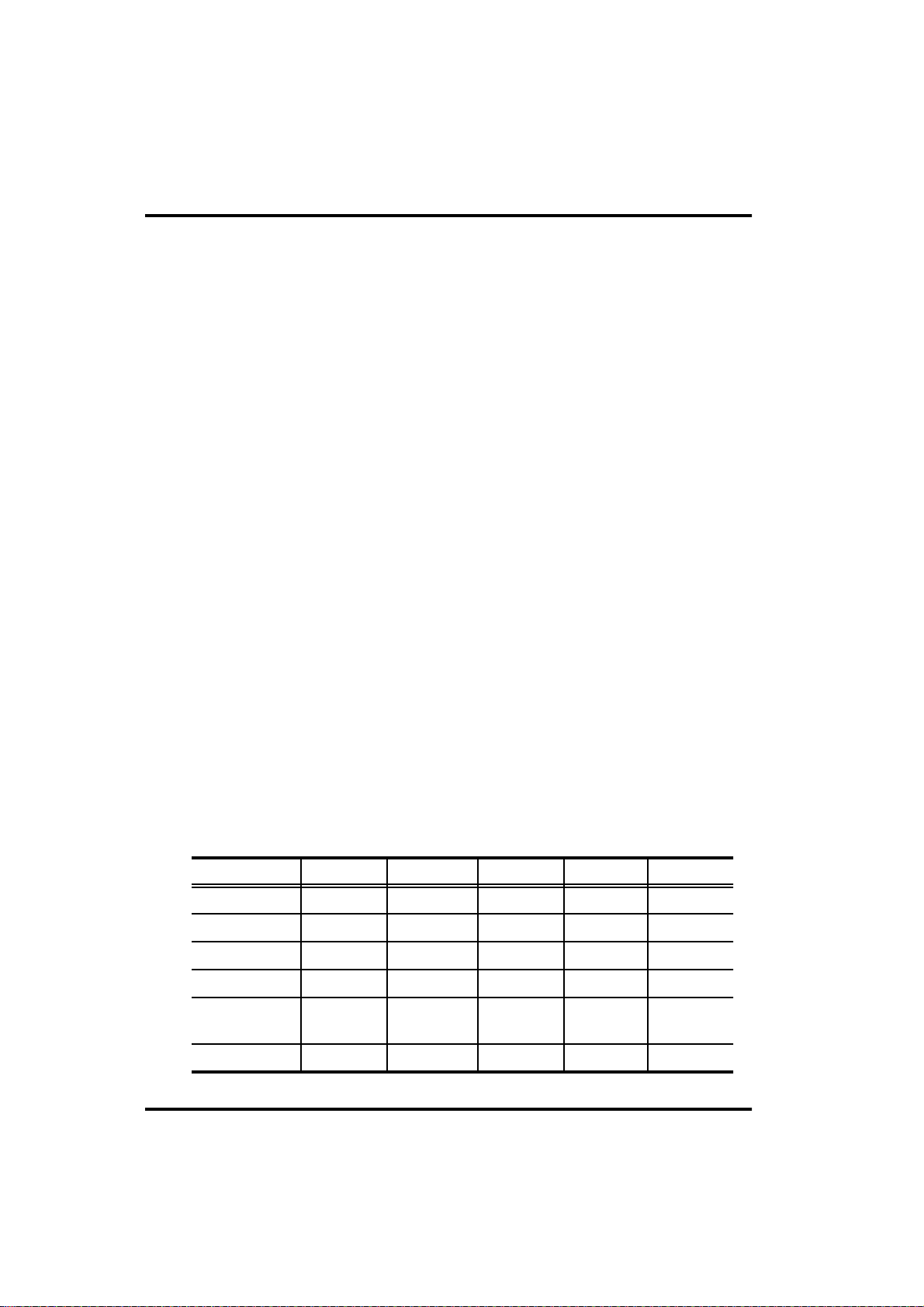
¡Ü Program memory : 512 bytes for GMS34004/012
1024 bytes for GMS34112/120/140
¡Ü Data memory : 32
¡Ü 43 types of instruction set
¡Ü 3 levels of subroutine nesting
¡Ü 1 bit output port for a large current (REMOUT signal)
¡Ü Operating frequency : 300~500KHz or 2.4~4MHz for 300~500KHz operation
(Masked option)
¡Ü Instruction cycle : f
¡Ü CMOS process (Single 3.0V power supply)
¡Ü Stop mode (Through internal instruction)
¡Ü Released stop mode by key input (Masked option)
¡Ü Built in capacitor for ceramic oscillation circuit (Masked option)
¡Ü Built in a watch dog timer (WDT)
¡Ü Low operating voltage : 2.0~4.0V (at 300~500KHz)
¡¿
4 bits
/6 (at 300~500KHz)
OSC
f
/48 (at 2.4~4MHz)
OSC
2.2~4.0V (at 2.4~4MHz)
Series
Program memory
Data memory
I/O ports
Input ports
Output ports
Package
GMS34004
512
32 ¡¿ 4
-
4
6
D0 ~ D5
16DIP/SOP
GMS34012
¡ç
¡ç
4
¡ç
6
D0 ~ D5
20DIP/SOP
GMS34112
1024
D0 ~ D5
Table 1-1 GMS340 series members
1 - 1
GMS34120
¡ç
¡ç
¡ç
¡ç
6
¡ç
¡ç
¡ç
¡ç
8
D0 ~ D7
24DIP/SOP
GMS34140
¡ç
¡ç
¡ç
¡ç
10
D0 ~ D9
¡ç
Page 7
Chapter 1. Introduction
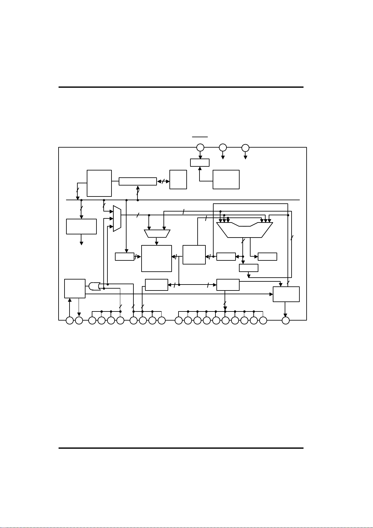
Block Diagram
RESET VDD GND
1 24
Reset
2
ROM
64word ¡¿
16page
¡¿
8
8
Instruction
Decoder
Control Signal
OSC
23 22 7 8 9 4 2110 3 5 6 11 12 13 14 15 16 17 18 19 20
OSC1 OSC2 K0 ~ K3 R0 ~ R3 D0 ~ D9 REMOUT
8bit
Program counter
4
MUX
X-Reg
4
10
4
2
4
4
10
Stack
4
MUX
RAM
RAM
16word x
2page x 4bit
R-Latch D-Latch
16
Word
Selector
4 10
Watchdog
timer
4
Y-Reg
4
10
ALU
4
ST
ACC
Pluse
Generator
Fig 1-1 Block Diagram (In case of GMS34140)
4
4
1 - 2
Page 8
Pin Assignment and terminals
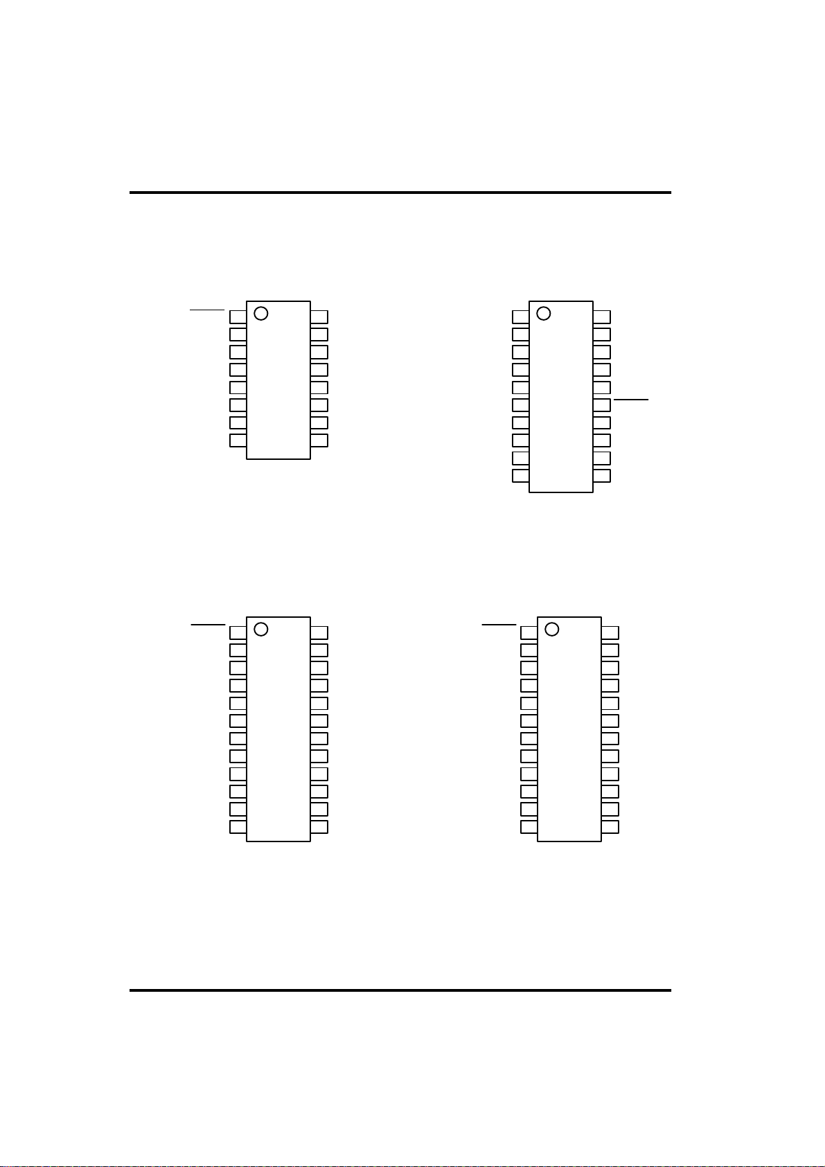
Pin Assignment
Chapter 1. Introduction
1 16
RESET
2 15
GND
3 14
K0
4 13
K1
5 12
K2
6 11
K3
7 10
D0
8 9
D1
VDD
OSC1
OSC2
REMOUT
D5
D4
D3
D2
1 20
K0
2 19
K1
3 18
K2
4 17
K3
5 16
D0
6 15
D1
7 14
D2
8 13
D3
9 12
D4
10 11
D5
R3
R2
R1
R0
GND
RESET
VDD
OSC1
OSC2
REMOUT
Fig 1-2 GMS34004 Pin Assignment Fig 1-3 GMS34012/112 Pin Assignment
1 24
RESET
2 23
GND
3 22
R0
4 21
R1
5 20
R2
6 19
R3
7 18
K0
8 17
K1
9 16
K2
10 15
K3
11 14
D0
12 13
NC
VDD
OSC1
OSC2
REMOUT
D7
D6
D5
D4
D3
D2
D1
NC
1 24
RESET
2 23
GND
3 22
R0
4 21
R1
5 20
R2
6 19
R3
7 18
K0
8 17
K1
9 16
K2
10 15
K3
11 14
D0
12 13
D8
VDD
OSC1
OSC2
REMOUT
D7
D6
D5
D4
D3
D2
D1
D9
Fig 1-5 GMS34120 Pin Assignment
Fig 1-6 GMS34140 Pin Assignment
1 - 3
Page 9
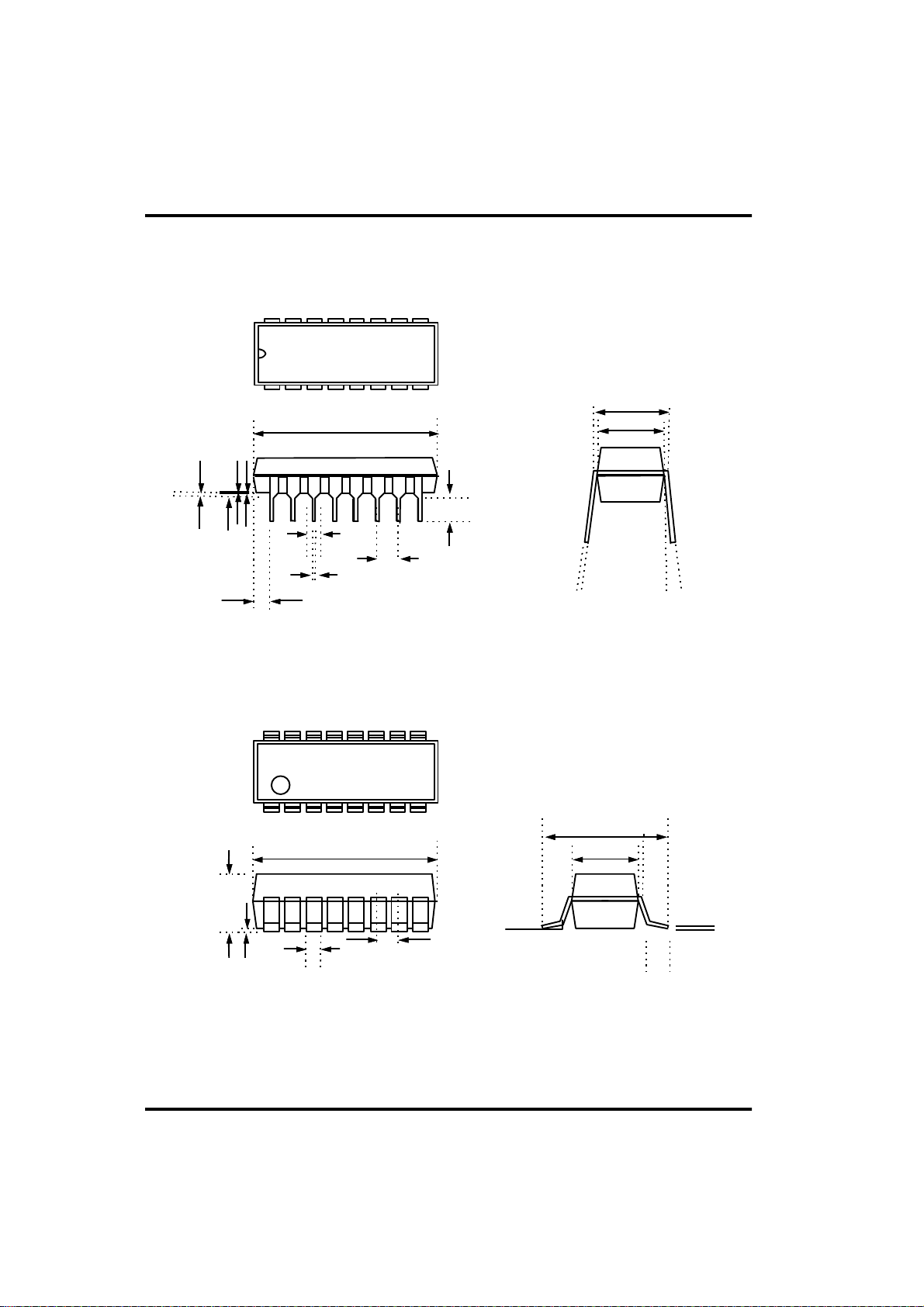
Pin Dimension
Chapter 1. Introduction
16 15 14 13 12 11 10 9
0.170MAX
0.0688MAX
1 2 3 4 5 6 7 8
0.785MAX
0.125MIN
0.135MAX
0.015MIN
0.040MAX
0.020MIN
16 15 14 13 12 11 10 9
1 2 3 4 5 6 7 8
0.0600MIN
0.745MIN
0.065MAX
0.050MIN
0.022MAX
0.015MIN
0.392MAX
0.386MIN
0.120MIN
0.140MAX
0.100BSC
Outline (Unit:Inch)
Fig 1-7 16PDIP Pin Dimension
¡æ ¡ç
0.244MAX
0.230MIN
0.157MAX
0.150MIN
0.300BSC
0.280MAX
0.240MIN
0.014MAX
0.008MIN
¡æ ¡ç
0~15¡Ç
Base Plane
Seating Plane
0.0040MIN
0.0098MAX
¡æ
¡ç
0.0200MAX
0.050BSC
¡Ç
0 ~ 8
Outline (Unit : Inch)
Fig 1-8 16SOP Pin Dimension (150Mil)
1 - 4
0.035MAX
0.016MIN
¡æ
¡ç
0.0098MAX
0.0075MIN
¡æ
¡ç
Page 10
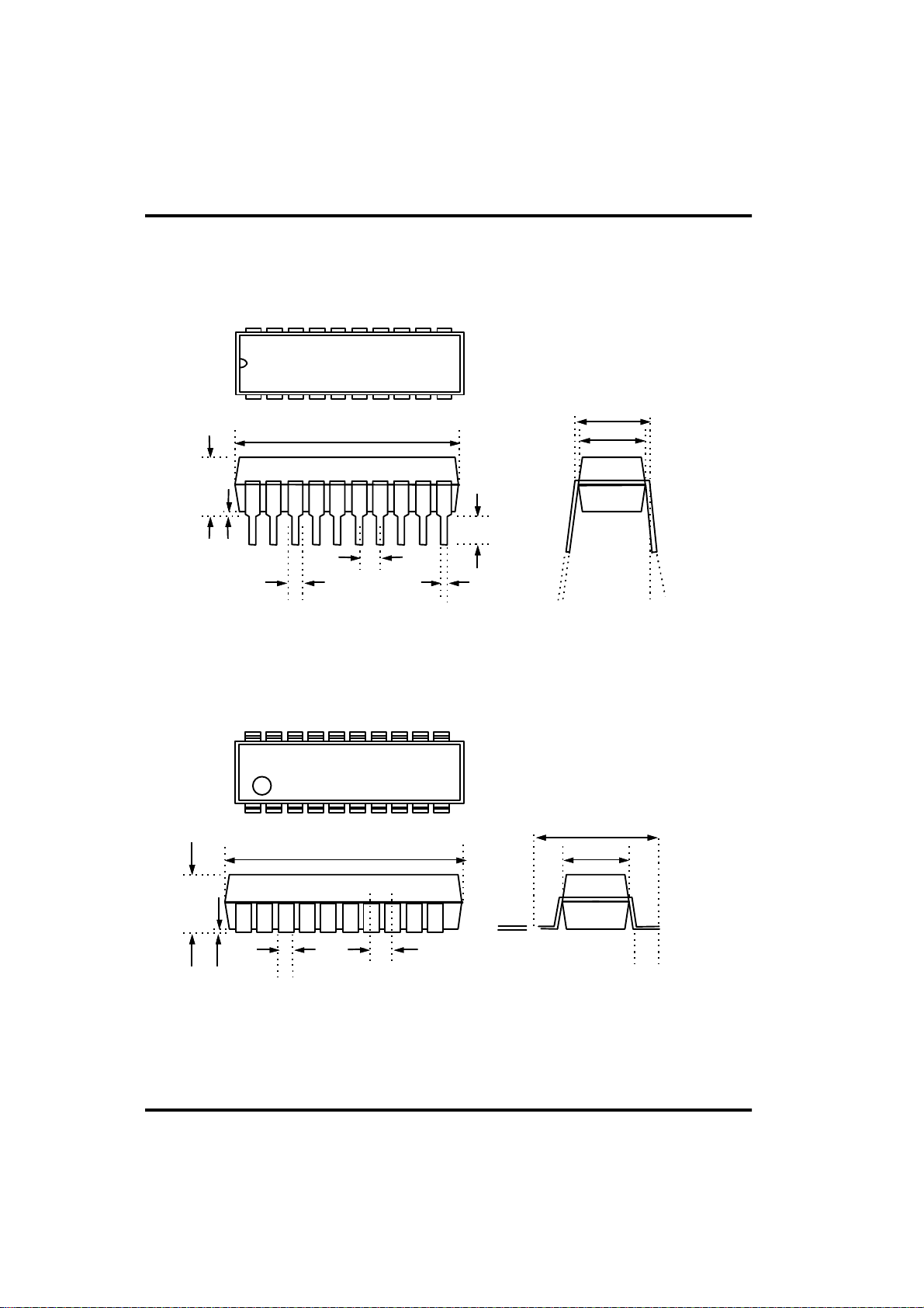
20 19 18 17 16 15 14 13 12 11
Chapter 1. Introduction
0.170MAX
0.104MAX
0.093MIN
1 2 3 4 5 6 7 8 9 10
0.984MAX
0.968MIN
0.065MAX
0.015MIN
0.055MIN
0.022MAX
0.015MIN
Outline (Unit : Inch)
Fig 1-10 20PDIP Pin Dimension
20 19 1 8 17 16 15 14 13 12 11
1 2 3 4 5 6 7 8 9 10
0.5118MAX
0.4961MIN
0.1TYP
0.125MIN
0.135MAX
¡æ ¡ç
0.299MAX
0.292MIN
0.3TYP
0.270MAX
0.250MIN
0.012MAX
0.008MIN
0.419MAX
0.398MIN
¡æ ¡ç
0~15¡Ç
0.004MIN
0.0118MAX
0.020MAX
0.014MIN
¡æ
¡ç
0.05TYP
Outline (Unit : Inch)
0.125MAX
0.0091MIN
Fig 1-11 20SOP Pin Dimension
1 - 5
¡æ
0.042MAX
¡ç
0.016MIN
Page 11
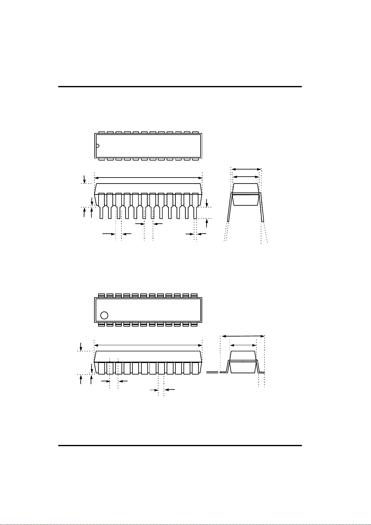
Chapter 1. Introduction
24 23 22 21 20 19 18 17 16 15 14
1 2 3 4 5 6 7 8 9 10 11
1.255MAX
1.245MIN
0.065MAX
0.055MIN
0.015MIN
0.170MAX
Outline (Unit : Inch)
Fig 1-12 24PDIP Pin Dimension
24 23 22 21 20 19 18 17 16 15 14
0.1TYP
0.022MAX
0.015MIN
13
12
0.125MIN
0.135MAX
¡æ ¡ç
13
0.3TYP
0.270MAX
0.250MIN
0.012MAX
0.008MIN
¡æ ¡ç
0~15¡Ç
0.104MAX
0.093MIN
0.018MAX
0.004MIN
1 2 3 4 5 6 7 8 9 10 11 12
0.618MAX
0.595MIN
0.05TYP
0.020MAX
0.014MIN
Outline (Unit : Inch)
Fig 1-13 24SOP Pin Dimension
1 - 6
¡æ
¡ç
0.125MAX
0.0091MIN
0.419MAX
0.396MIN
0.299MAX
0.292MIN
¡æ
0.042MAX
¡ç
0.016MIN
Page 12
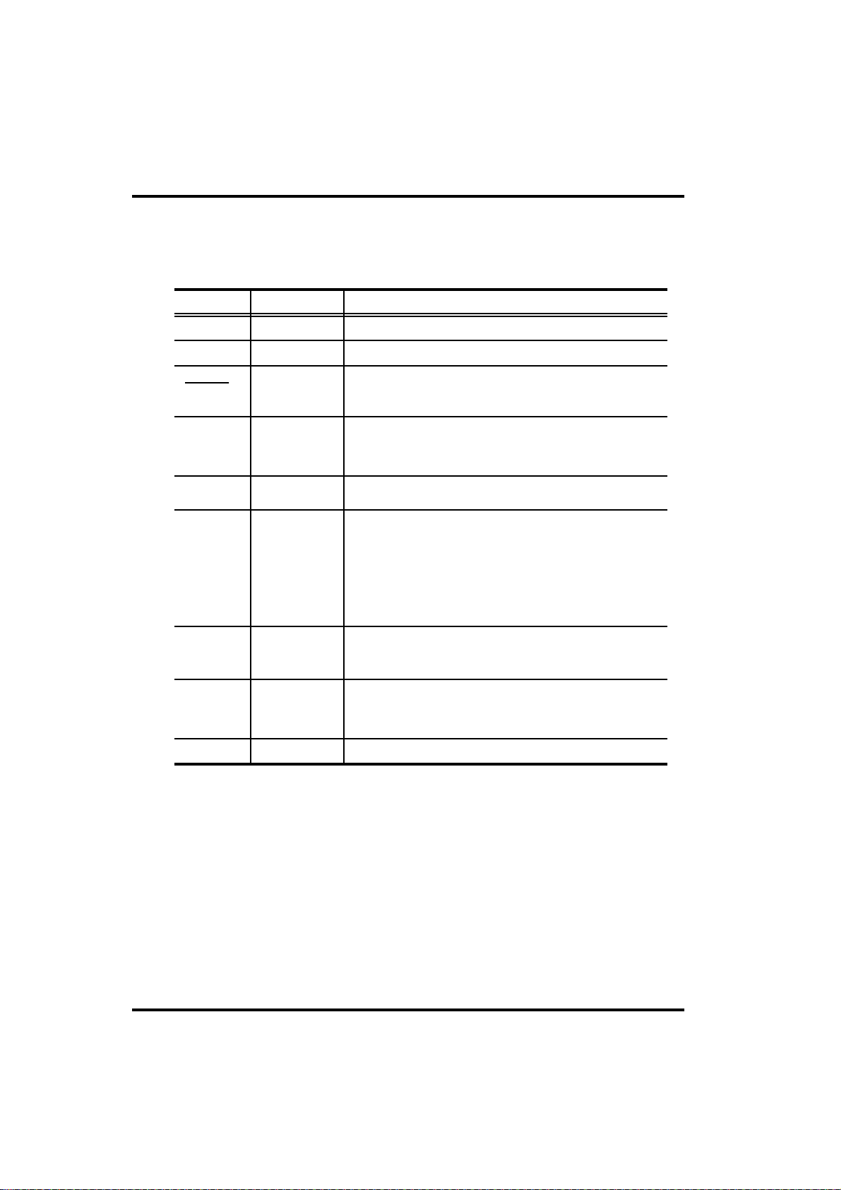
Chapter 1. Introduction
I/O circuit types and options
GMS340 series I/O port types
Pin Function
V
DD
GND
RESET
K0~K3
D0~D9
R0~R3
REMOUT
OSC1
OSC2
I/O
-
-
Input
Input
Output
I/O
Output
Input
Output
Connected to 2.0~4.0V power supply.
Connected to 0V power supply.
Used to input a manual reset. When the pin goes ¡ÈL¡È, the
D-output ports and REMOUT-output port are initialized to
¡ÈL¡È
, and ROM address is set to address 0 on page 0.
4-bit input port.
Released STOP mode built in pull-up resistor by each pin as
masked option.
(It is released by ¡ÈL¡È input at STOP)
Each can be set and reset independently. The output is in
the form of N-channel-open-drain.
4-bit I/O port. (Input mode is set only when each of them
output ¡ÈH¡È.)
In outputting, each can be set and reset independently(or at
once.)
The output is in the form of N-channel-open-drain.
Pull-up resistor and STOP release mode can be respectively
selected as masked option for each bit. (It is released by
¡ÈL¡È
input at STOP.)
High current output port.
The output is in the form of C-MOS.
The state of large current on is ¡ÈH¡È.
Oscillator input. Input to the oscillator circuit and connection
point for ceramic resonator.
Internal capacitors available as masked option.
A feedback resistor is connected between this pin and OSC2
Connect a ceramic resonator between this pin and OSC1.
1 - 7
Page 13
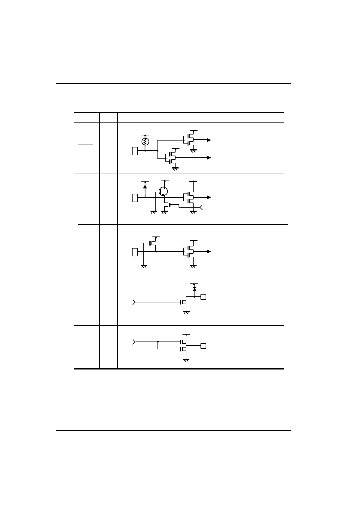
I/O circuit types and options
Chapter 1. Introduction
Pin I/O Note
Reset I
R0~R3 I/O
K0~K3 I
¡æ
I/O circuit
¡æ
¡ç
¡æ
¡æ
¡æ
¡ç
¡æ
¡ç
¡æ
¡ç
Hysteresis Input Type
Built in pull-upresistor Typical 400
(option)
Built in pull-up
resistor
Typical 800
Open drain output
¡ÈH¡È
(Option)
Built in MOS Tr for
pull-up About 120
Built in MOS Tr for
pull-up About 120
§Ú
§Ú
output at reset
§Ú
§Ú
D0~D9
REMOUT O
O
¡ç
¡æ
¡ç
1 - 8
Open drain output
¡ÈL¡È
output at reset
CMOS output
¡ÈL¡È
output at reset
High current source
output
Page 14
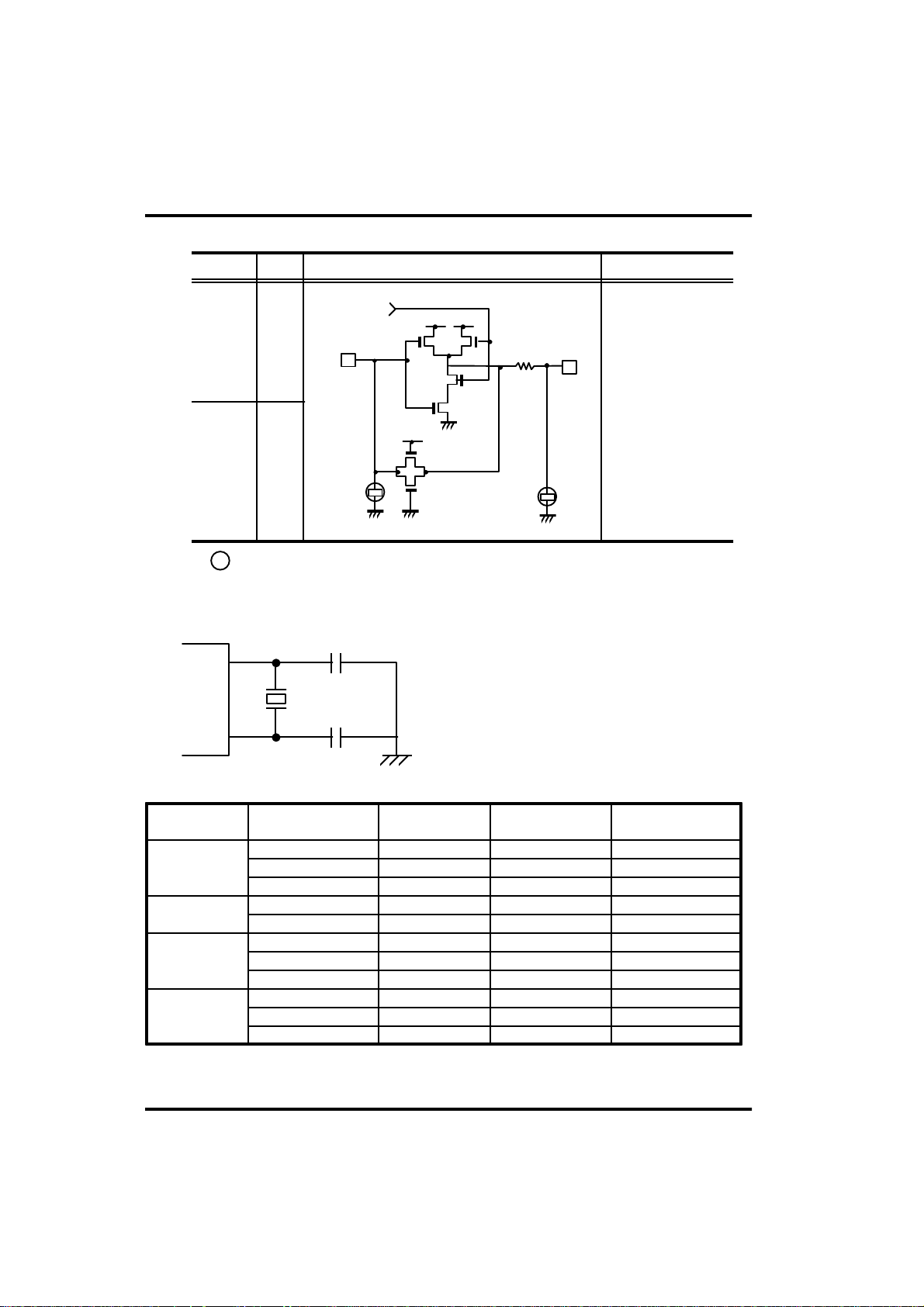
Chapter 1. Introduction
Pin I/O Note
OSC2 O
OSC1 I
: Masked option
*. Recommendable circuit
OSC1
OSC2
OSCSTB
OSC1
C1
C2
C1
I/O circuit
¡æ
¡è
¡è
Rf
¡ç
¡æ
¡ç
Rd
C2
OSC2
Built in feedbackResister About 1
Built in dumping-Resister
[No resistor in MHz
operation]
(Option)
Built in resonance
Capacitor
C1/C2 = 100pF
N%
[C1/C2 are not
available for MHz
operation]
§Û
¡¾
Frequency Resonator Maker Part Name Load Capacitor Operating Voltage
Murata CSB455E C1=C2=Open 2.0 ~ 4.0V
455KHz
480KHz
3.64MHz
3.84MHz
¡Ø
CST type is building in load capacitior
Kyocera KBR-455BKTL70 C1=C2=Open 2.0 ~ 4.0V
TDK FCR455K3 C1=C2=Open 2.0 ~ 4.0V
Murata
TDK FCR480K3 C1=C2=Open 2.0 ~ 4.0V
Murata CSA3.64MG C1=C2=30pF 2.2 ~ 4.0V
Murata CST3.64MGW C1=C2=Open 2.2 ~ 4.0V
TDK FCR3.64MC5 C1=C2=Open 2.2 ~ 4.0V
Murata CSA3.84MG C1=C2=30pF 2.2 ~ 4.0V
Murata CST3.84MGW C1=C2=Open 2.2 ~ 4.0V
TDK FCR3.84MC5 C1=C2=Open 2.2 ~ 4.0V
CSB480E C1=C2=Open 2.0 ~ 4.0V
1 - 9
Page 15
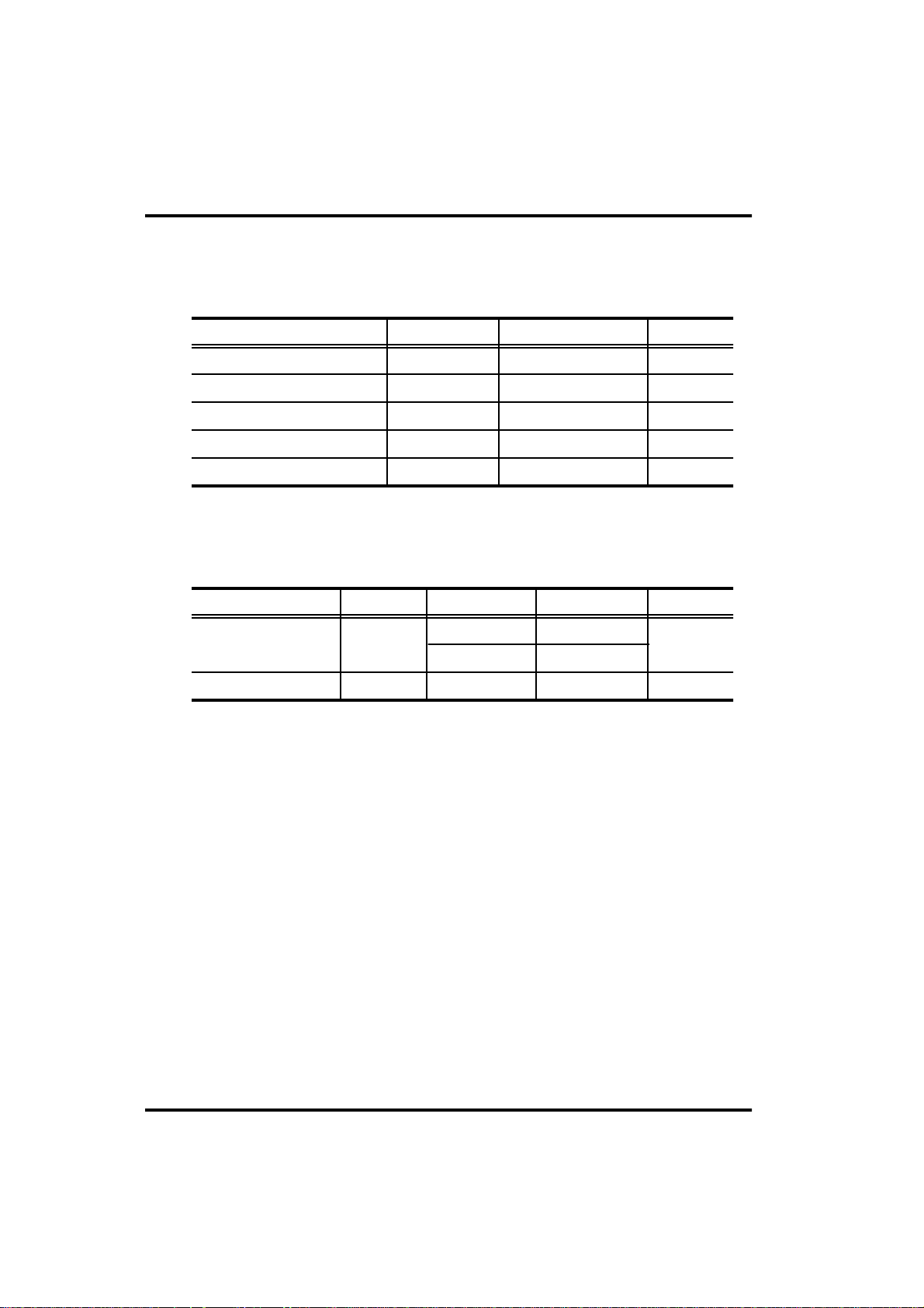
Chapter 1. Introduction
Electrical Characteristics for GMS300 series
Absolute maximum ratings (Ta = 25¡É)
Parameter
Supply Voltage
Power dissipation
Storage temperature range
Input voltage
Output voltage
* Thermal derating above 25¡É : 6mW per degree ¡É rise in temperature.
Recommended operation condition
Parameter
Supply Voltage
Operating temperature
Symbol
V
DD
Topr
Symbol
V
DD
P
D
Tstg
V
IN
V
OUT
Condition
300 ~ 500KHz
2.4 ~ 4MHz
Max. rating
-0.3 ~ 5.0
¡É
700
-55 ~ 125
-0.3 ~ VDD+0.3
-0.3 ~ VDD+0.3
Rating
2.0 ~ 4.0
2.2 ~ 4.0
-
-20 ~ +70
Unit
V
mW
¡É
V
V
Unit
V
¡É
1 - 10
Page 16
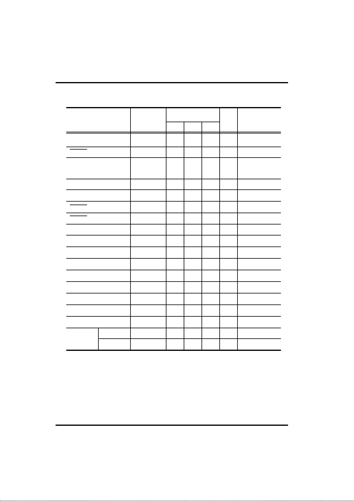
Electrical characteristics (Ta=25¡É, VDD=3V)
Chapter 1. Introduction
Parameter
Input H current
RESET input L current
K, R input L current
K, R input H voltage
K, R input L voltage
RESET input H voltage
RESET input L voltage
D. R output L voltage
REMOUT output L
voltage
REMOUT output H
voltage
OSC2 output L voltage
OSC2 output H voltage
D, R output leakage
current
Current on STOP mode
Operating supply current
1
Operating supply current
2
System
clock
frequency
f
/6
OSC
f
/48 f
OSC
Symbol
I
IH
I
IL2
I
IL1
V
IH1
V
IL1
V
IH2
V
IL2
V
OL2
V
OL1
V
OH1
V
OL3
V
OH3
I
OL
I
STOP
I
DD1
I
DD2
f
OSC
OSC
Limits
Min. Typ. Max.
1
-
-16
-50
-
-
0.9
-
-
-
0.7
5
0.4
5
0.4
5
-
0.9
-
1
1
-
1.0
1.5
500
4
-
-2
-9
2.1
2.2
5
2.1
2.1
300
2.4
-
-7.5
-25
-
-
-
0.1
-
0.1
2.5
-
0.4
2.5
-
-
-
0.3
-
0.5
Unit Condition
uA
VI=V
DD
uA
VI=GND
VI=GND, Output
uA
off, Pull-Up resistor
provided.
V
-
V
-
V
-
V
V
V
IOL=1mA
V
IOL=100uA
V
IOH=8mA
V
IOL=70uA
V
IOH=70uA
uA
V0=VDD, Output
off
uA
At STOP mode
mA
f
=455KHz
OSC
mA
f
=4MHz
OSC
KHz
MHz
1 - 11
Page 17
INTRODUCTION 1
ARCHITECTURE 2
INSTRUCTION 3
EVALUATION BOARD 4
SOFTWARE 5
APPENDIX 6
Page 18
CHAPTER 2. Architecture
BLOCK DESCRIPTION
Characteristics
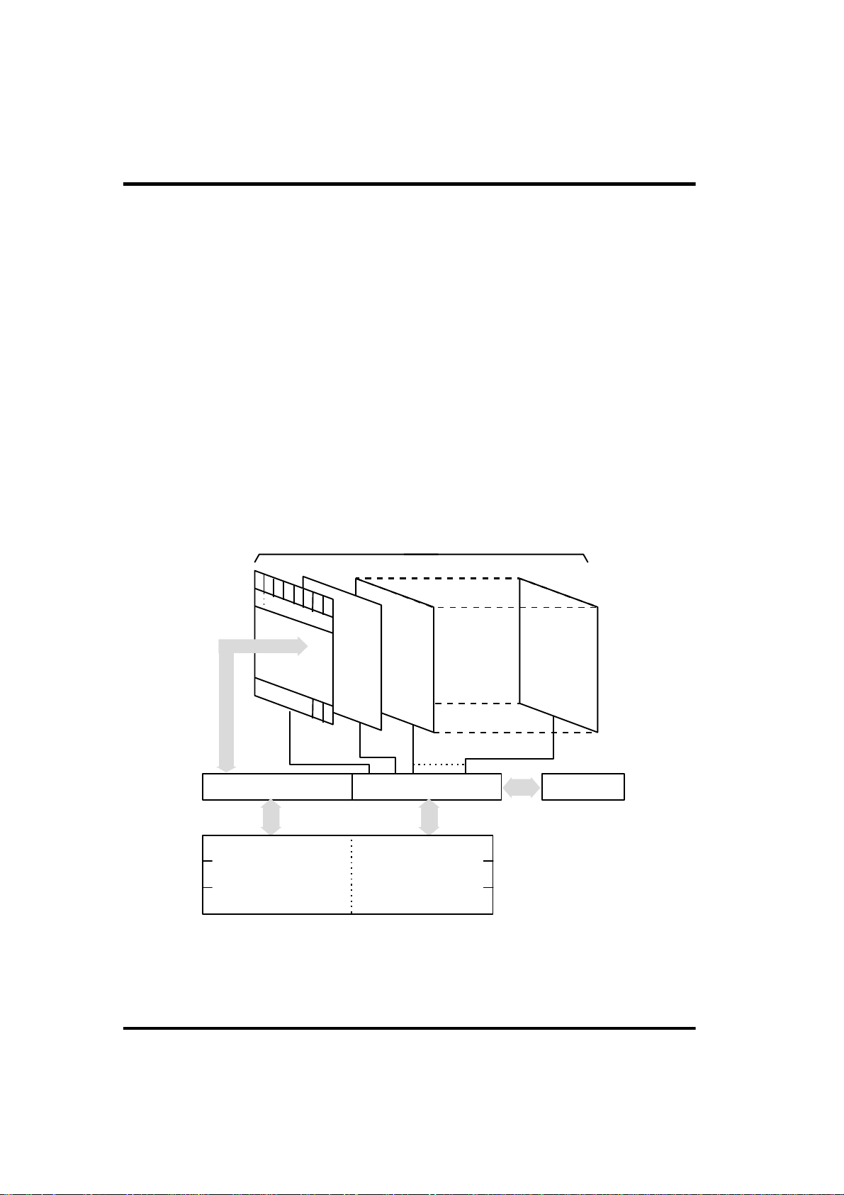
The GMS340 series can incorporate maximum 1024 words (64 words ¡¿ 16
pages ¡¿ 8bits) for program memory. Program counter PC (A0~A5) and page
address register (A6~A9) are used to address the whole area of program
memory having an instruction (8bits) to be next executed.
The program memory consists of 64 words on each page, and thus each page
can hold up to 64 steps of instructions.
The program memory is composed as shown below.
0
1
2
3
4
8
5
6
7
Chapter 2. Architecture
Program capacity (pages)
Page 0 Page 1 Page 2 Page 15
63
A0~A5
Program counter (PC) Page address register (PA) Page buffer (PB)
0 1 2 15
6 4
Stack register
(Level ¡È1¡È)
(Level ¡È2¡È)
(Level ¡È3¡È)(PRS)(SR)
A6~A9
Fig 2-1 Configuration of Program Memory
2 - 1
Page 19

Chapter 2. Architecture
ROM Address Register
The following registers are used to address the ROM.
• Page address register (PA) :
Holds ROM`s page number (0~Fh) to be addressed.
• Page buffer register (PB) :
Value of PB is loaded by an LPBI command when newly addressing a page.
Then it is shifted into the PA when rightly executing a branch instruction (BR)
and a subroutine call (CAL).
• Program counter (PC) :
Available for addressing word on each page.
• Stack register (SR) :
Stores returned-word address in the subroutine call mode.
(1) Page address register and page buffer register :
Address one of pages #0 to #15 in the ROM by the 4-bit binary counter.
Unlike the program counter, the page address register is usually unchanged
so that the program will repeat on the same page unless a page changing
command is issued. To change the page address, take two steps such as
(1) writing in the page buffer what page to jump to (execution of LPBI) and
(2) execution of BR or CAL, because and instruction code is of eight bits so
that page and word cannot be specified at the same time.
In case a return instruction (RTN) is executed within the subroutine that has
been called in the other page, the page address will be changed at the
same time.
(2) Program counter :
This 6-bit binary counter increments for each fetch to address a word in the
currently addressed page having an instruction to be next executed.
For easier programming, at turning on the power, the program counter is
reset to the zero location. The PA is also set to ¡È0¡È. Then the program
counter specifies the next ROM address in random sequence.
When BR, CAL or RTN instructions are decoded, the switches on each step
are turned off not to update the address. Then, for BR or CAL, address
data are taken in from the instruction operands (a0 to a5), or for RTN, and
address is fetched from stack register No. 1.
(3) Stack register :
This stack register provides two stages each for the program counter (6
bits) and the page address register (4bits) so that subroutine nesting can be
mode on two levels.
2 - 2
Page 20
Chapter 2. Architecture
Data memory (RAM)
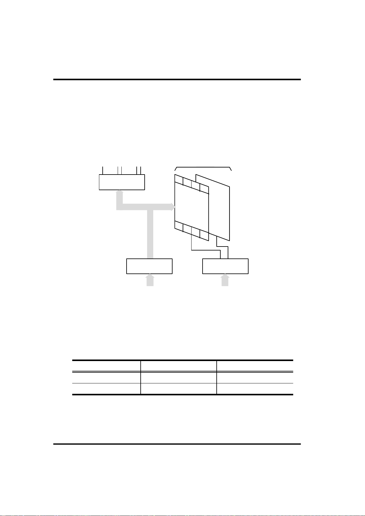
Up to 32 nibbles (16 words ¡¿ 2pages ¡¿ 4bits) is incorporated for storing data.
The whole data memory area is indirectly specified by a data pointer (X,Y). Page
number is specified by zero bit of X register, and words in the page by 4 bits in
Y-register. Data memory is composed in 16 nibbles/page. Figure 2.2 shows the
configuration.
X-register (X)
D0 D9 R0 R3 REMOUT
Output port
Y-register (Y) X-register (X)
4 2
Fig 2-2 Composition of Data Memory
Data memory page (0~1)
0
1
2
3
Page 0 Page 1
15
0 14 A0~A3
X-register is consist of 2bit, X0 is a data pointer of page in the RAM, X1 is only
used for selecting of D8~D9 with value of Y-register
X1=1X1=0
Y=0
Y=1 D1
D0
Table 2-1 Mapping table between X and Y register
2 - 3
D8
D9
Page 21

Chapter 2. Architecture
Y-register (Y)
Y-register has 4 bits. It operates as a data pointer or a general-purpose register.
Y-register specifies and address (a0~a3) in a page of data memory, as well as it
is used to specify an output port. Further it is used to specify a mode of carrier
signal outputted from the REMOUT port. It can also be treated as a generalpurpose register on a program.
Accumulator (ACC)
The 4-bit register for holding data and calculation results.
Arithmetic and Logic Unit (ALU)
In this unit, 4bits of adder/comparator are connected in parallel as it`s main
components and they are combined with status latch and status logic (flag.)
(1) Operation circuit (ALU) :
The adder/comparator serves fundamentally for full addition and data
comparison. It executes subtraction by making a complement by processing
an inversed output of ACC (ACC+1)
(2) Status logic :
This is to bring an ST, or flag to control the flow of a program. It occurs when
a specified instruction is executed in two cases such as overflow in operation
and two inputs unequal.
2 - 4
Page 22
Chapter 2. Architecture
State Counter (SC)
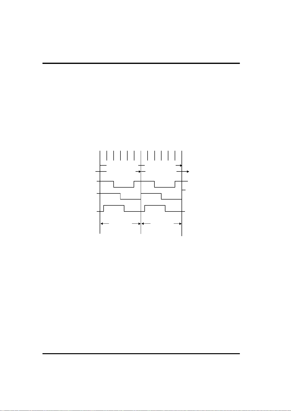
A fundamental machine cycle timing chart is shown below. Every instruction is
one byte length. Its execution time is the same. Execution of one instruction
takes 6 clocks for fetch cycle and 6 clocks for execute cycle (12 clocks in total).
Virtually these two cycles proceed simultaneously, and thus it is apparently
completed in 6 clocks (one machine cycle). Exceptionally BR, CAL and RTN
instructions is normal execution time since they change an addressing
sequencially. Therefore, the next instruction is prefetched so that its execution
is completed within the fetch cycle.
T1 T2 T3 T4 T5 T6 T1 T2 T3 T4 T5 T6
Phase
Phase
Phase
Fetch cycle N
Execute cycle N-1
¥°
¥±
¥²
Machine
Cycle
Fig. 2-3 Fundamental timing chart
Execute cycle N
Fetch cycle N-1
Machine
Cycle
2 - 5
Page 23
Chapter 2. Architecture
Clock Generator
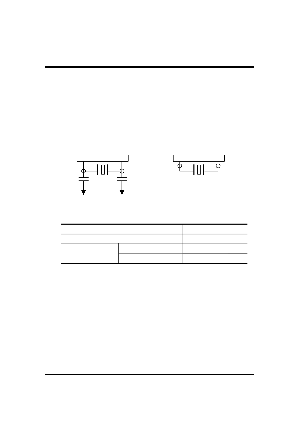
The GMS340 series has an internal clock oscillator. The oscillator circuit is
designed to operate with an external ceramic resonator. Internal capacitors are
available as a masked option. Oscillator circuit is able to organize by connecting
ceramic resonator to outside. (In order to built in capacitor for oscillation as
masked option.)
* It is necessary to connect capacitor to outside in order to change ceramic
resonator, You must examine refer to a manufacturer`s
OSC1 OSC2
23 22
C1 C2
<Circuit 1>
Operating Frequency
f
= 2.4 ~ 4MHz
OSC
f
= 300 ~ 500KHz
OSC
Internal capacitor option
No Internal capacitor option Circuit 1
OSC1 OSC2
23 22
<Circuit 2>
Oscillation Circuit
Circuit 1
Circuit 2
2 - 6
Page 24
Chapter 2. Architecture
Pulse generator
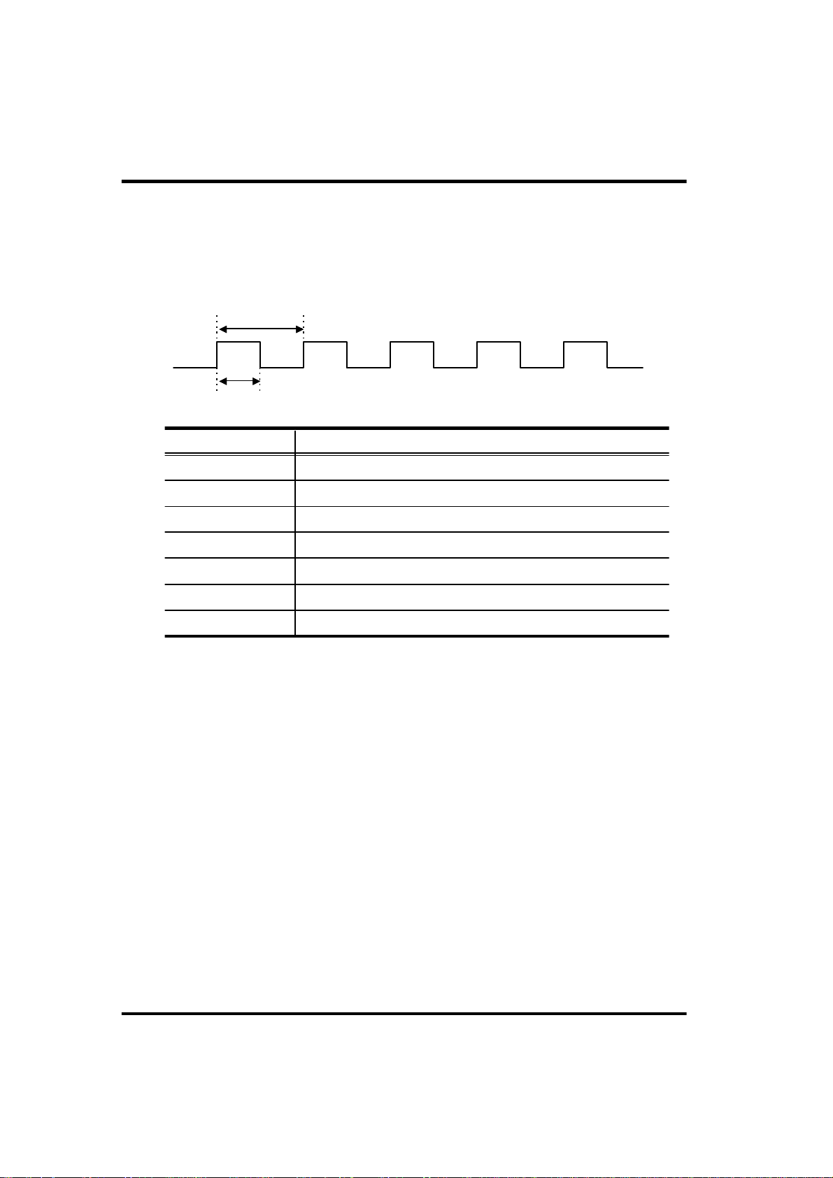
The following frequency and duty ratio are selected for carrier signal outputted
from the REMOUT port depending on a PMR (Pulse Mode Register) value set in
a program.
T
T1
PMR
1
2
3
4
5
6 T=1/f
* Default value is ¡È0
T=1/f
= 12/f
PUL
T=1/f
= 12/f
PUL
T=1/f
= 8/f
PUL
OSC
T=1/f
= 8/f
PUL
OSC
T=1/f
= 11/f
PUL
No Pulse (same to D0~D9)
= 12/f
PUL
¡È
REMOUT signal
[96/f
OSC
OSC
[96/f
OSC
OSC
[64/f
], T1/T = 1/2
OSC
[64/f
], T1/T = 1/4
OSC
[88/f
OSC
OSC
[96/f
OSC
OSC
], T1/T = 1/20
], T1/T = 1/3
], T1/T = 4/11
], T1/T = 1/4
* [ ] means the value of ¡ÈT¡È, when Instruction cycle is f
Table 2-2 PMR selection table
OSC
/48
2 - 7
Page 25
Chapter 2. Architecture
Initial Reset Circuit
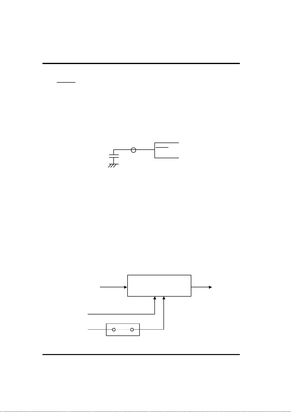
RESET pin must be down to ¡ÈL¡È more than 4 machine cycle by outside
capacitor or other for power on reset.
The mean of 1 machine cycle is below. 1 machine cycle is 6/f
operating voltage must be in recommended operating conditions, and clock
oscillating stability.
* It is required to adjust C value depending on rising time of power supply.
(Example shows the case of rising time shorter than 10ms.)
1
RESET
0.1uF
Watch Dog Timer (WDT)
Watch dog timer is organized binary of 14 steps. By the selected oscillation
option, the signal of f
/6 cycle comes in the first step of WDT. If this counter
OSC
was overflowed, come out reset signal automatically, internal circuit is initialized.
The overflow time is 6¡¿2 13/f
8¡¿6¡¿213/f
(108.026ms at f
OSC
(108.026ms at f
OSC
=455KHz.)
OSC
OSC
= 3.64MHz)
Normally, the binary counter must be reset before the overflow by using reset
instruction (WDTR) or / and REMOUT port (Y-reg=8, So instruction execution) at
masked option.
, however,
OSC
* It is constantly reset in STOP mode. When STOP is released, counting is
restarted. (Refer to 2-10 STOP function>)
Binary counter
(14 steps)
Reset
by instruction
REMOUT
output
f
OSC
/6 or f
OSC
/48
RESET (edge-trigger)
Mask Option
2 - 8
CPU reset
Page 26

Chapter 2. Architecture
STOP Function
Stop mode can be achieved by STOP instructions.
In stop mode :
1. Oscillator is stopped, the operating current is low.
2. Watch dog timer is reset, D8~D9 output and REMOUT output are ¡ÈL¡È.
3. Part other than WDT, D8~D9 output and REMOUT output have a value before
come into stop mode.
¡ÈBut, the state of D0~D7 output in stop mode is able to choose as masked
option. ¡ÈL¡È output or same level before come into stop mode.
The function to release stop mode is able to choose each bit of K or R input.
Stop mode is released when one of K or R input is going to ¡ÈL¡È.
1. State of D0~D7 output and REMOUT output is return to state of before stop mode
is achieved.
2. After 1024¡¿8 enable clocks for stable oscillating. First instruction start to operate.
3. In return to normal operation, WDT is counted from zero again.
But, at executing stop instruction, if one of K or R input is chosen to ¡ÈL¡È, stop
instruction is same to NOP instruction.
Masked options
The GMS340 series offer the following optional features.
These options are masked.
1. Watch dog timer reset by REMOUT output signal.
2. Input terminals having STOP release mode : K0~K3, R0~R3.
3. I/O terminals having pull-up resistor : R0~R3
4. Ceramic oscillation circuit contained (or not contained).
[This option is not available for MHz Ceramic oscillator]
5. Output form at stop mode
D0~D7 : ¡ÈL¡È or keep before stop mode
6. Instruction cycle selection:
T=48/f
OSC
or T=6/f
OSC
2 - 9
Page 27
INTRODUCTION 1
ARCHITECTURE 2
INSTRUCTION 3
EVALUATION BOARD 4
SOFTWARE 5
APPENDIX 6
Page 28

CHAPTER 3. Instruction
INSTRUCTION FORMAT
All of the 43 instruction in GMS340 series is format in two fields of OP code and
operand which consist of eight bits. The following formats are available with
different types of operands.
Chapter 3. Instruction
Format
Format
Format
Format
¥°
All eight bits are for OP code without operand.
¥±
Two bits are for operand and six bits for OP code.
Two bits of operand are used for specifying bits of RAM and X-register (bit 1 and
bit 7 are fixed at ¡È0¡È)
¥²
Four bits are for operand and the others are OP code.
Four bits of operand are used for specifying a constant loaded in RAM or Yregister, a comparison value of compare command, or page addressing in ROM.
¥³
Six bits are for operand and the others are OP code.
Six bits of operand are used for word addressing in the ROM.
3 - 1
Page 29
Chapter 3. Instruction
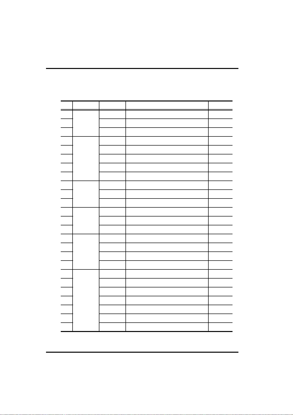
INSTRUCTION TABLE
The GMS340 series provides the following 43 basic instructions.
1
2
3
4
5
6
7
8
9
10
11
12
13
14
15
16
17
Category
Register to
Register
RAM to
Register
Immediate
RAM Bit
Manipulation
ROM
Address
Mnemonic
LAY
LYA
LAZ
LMA
LMAIY
LYM
LAM
XMA
LYI i
LMIIY i
LXI n
SEM n
REM n
TM n
BR a
CAL a
RTN
Function
A ¡ç Y
Y ¡ç A
A ¡ç 0
M(X,Y) ¡ç A
M(X,Y) ¡ç A, Y ¡ç Y+1
Y ¡ç M(X,Y)
A ¡ç M(X,Y)
A ¡ê M(X,Y)
Y ¡ç i
M(X,Y) ¡ç i, Y ¡ç Y+1
X ¡ç n
M(n) ¡ç 1
M(n) ¡ç 0
TEST M(n) = 1
if ST = 1 then Branch
if ST = 1 then Subroutine call
Return from Subroutine
ST
*1
S
S
S
S
S
S
S
S
S
S
S
S
S
E
S
S
S
18 LPBI i PB ¡ç i S
19
20
21
22
23
24
25
Arithmetic
AM
SM
IM
DM
IA
IY
DA
A ¡ç A + M(X,Y)
A ¡ç M(X,Y) - A
A ¡ç M(X,Y) + 1
A ¡ç M(X,Y) - 1
A ¡ç A + 1
Y ¡ç Y + 1
A ¡ç A - 1
3 - 2
C
B
C
B
S
C
B
Page 30
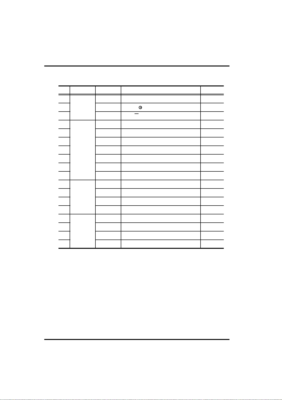
Chapter 3. Instruction
Category
26
Arithmetic
27
28
29
30
31
Comparison
32
33
34
35 RNEZ TEST R ¡Á 0 N
36
37
38
39
40
41
42
Input /
Output
Control
Mnemonic
DY
EORM
NEGA
ALEM
ALEI i
MNEZ
YNEA
YNEI i
KNEZ
LAK
LAR
SO
RO
WDTR
STOP
LPY
Function
Y ¡ç Y - 1
A ¡ç A + M (X,Y)
A ¡ç A + 1
TEST A ¡Â M(X,Y)
TEST A ¡Â i
TEST M(X,Y) ¡Á 0
TEST Y ¡Á A
TEST Y ¡Á i
TEST K ¡Á 0
A ¡ç K
A ¡ç R
Output(Y) ¡ç 1
Output(Y) ¡ç 0
Watch Dog Timer Reset
Stop operation
PMR ¡ç Y
*2
*2
ST
*1
B
S
Z
E
E
N
N
N
N
S
S
S
S
S
S
S
43
NOP
No operation
S
Note) i = 0~f, n = 0~3, a = 6bit PC Address
*1 Column ST indicates conditions for changing status. Symbols have the following
meanings
S : On executing an instruction, status is unconditionally set.
C : Status is only set when carry or borrow has occurred in operation.
B : Status is only set when borrow has not occurred in operation.
E : Status is only set when equality is found in comparison.
N : Status is only set when equality is not found in comparison.
Z : Status is only set when the result is zero.
3 - 3
Page 31
Chapter 3. Instruction
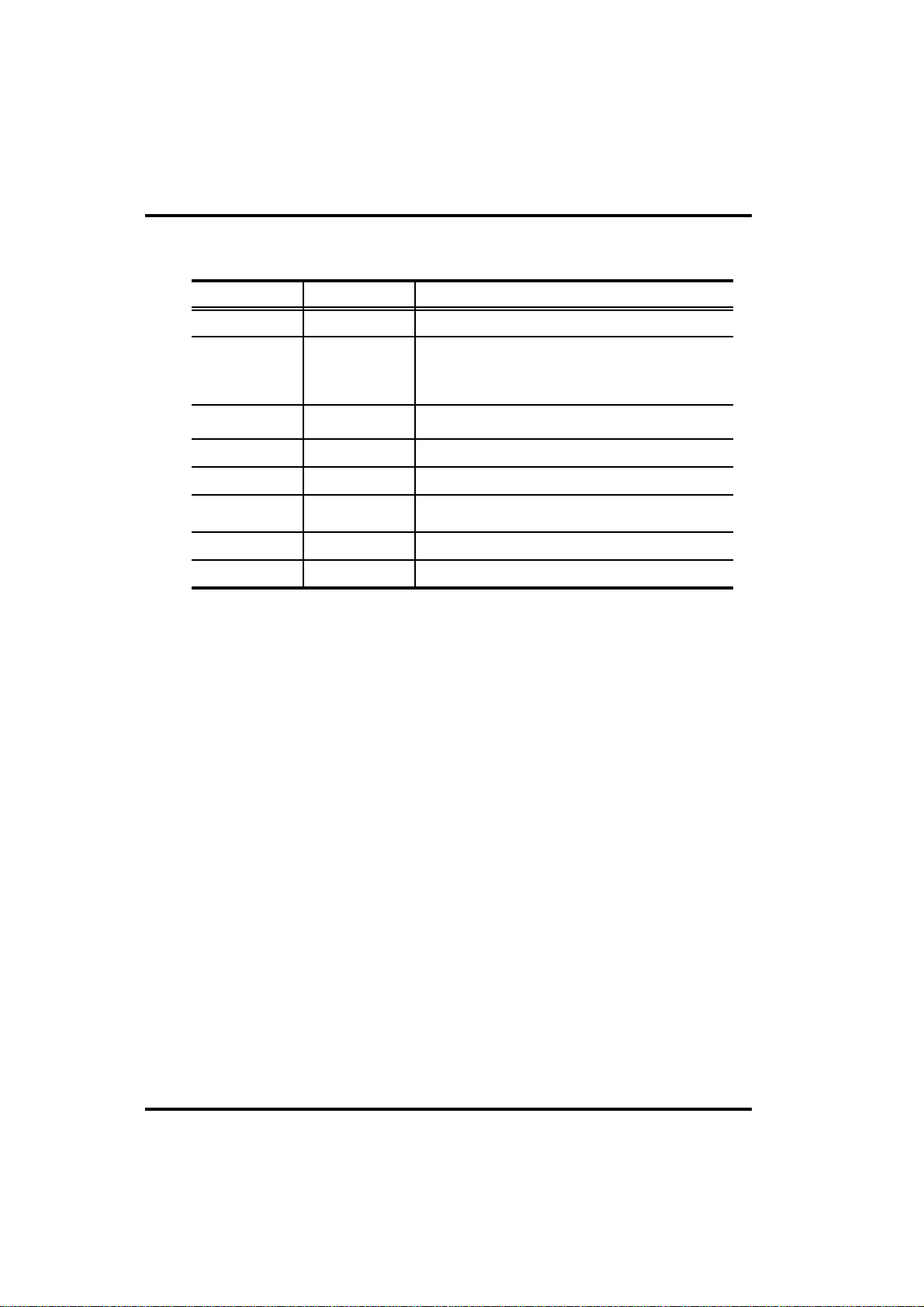
*2 Operation is settled by a value of Y-register.
Value of X-reg
0 or 1 SO : D(Y) ¡ç 1, RO : D(Y) ¡ç 0
0 or 1 8
0 or 1
0 or 1 SO : R(Y-Ah) ¡ç 1, RO : R(Y-Ah) ¡ç 0A ~ D
0 or 1 SO : R0 ~ R3 ¡ç 1, RO : R0~R3 ¡ç 0E
0 or 1
2 or 3 SO : D(8) ¡ç 1, RO : D(8) ¡ç 00
2 or 3 SO : D(9) ¡ç 1, RO : D(9) ¡ç 01
Value of Y-reg
0~7
9
F
REMOUT port repeats ¡ÈH¡È and ¡ÈL¡È in pulse
frequency. (when PMR = 5, it is fixed at ¡ÈH¡È)
SO : REMOUT (PMR) ¡ç 1
RO : REMOUT (PMR) ¡ç 0
SO : D0 ~ D9 ¡ç 1 (High-Z)
R0 : D0 ~ D9 ¡ç 0
SO : D0 ~ D9 ¡ç 1 (High-Z) R0~R3 ¡ç 1
R0 : D0 ~ D9 ¡ç 0 R0~R3 ¡ç 0
Operation
3 - 4
Page 32

DETAILS OF INSTRUCTION SYSTEM
All 43 basic instructions of the GMS340 Series are one by one described in detail
below.
Description Form
Each instruction is headlined with its mnemonic symbol according to the
instructions table given earlier.
Then, for quick reference, it is described with basic items as shown below. After
that, detailed comment follows.
• Items :
- Naming : Full spelling of mnemonic symbol
- Status : Check of status function
- Format : Categorized into ¥° to
- Operand : Omitted for Format
- Function
Chapter 3. Instruction
¥³
¥°
3 - 5
Page 33

Chapter 3. Instruction
Detailed Description
(1) LAY
Naming : Load Accumulator from Y-Register
Status : Set
Format : I
Function : A ¡ç Y
<Comment> Data of four bits in the Y-register is unconditionally transferred
(2) LYA
Naming : Load Y-register from Accumulator
Status : Set
Format : I
Function : Y ¡ç A
<Comment> Load Y-register from Accumulator
(3) LAZ
Naming : Clear Accumulator
Status : Set
Format : I
Function : A ¡ç 0
<Comment> Data in the accumulator is unconditionally reset to zero.
to the accumulator. Data in the Y-register is left unchanged.
(4) LMA
Naming : Load Memory from Accumulator
Status : Set
Format : I
Function : M(X,Y) ¡ç A
<Comment> Data of four bits from the accumulator is stored in the RAM
location addressed by the X-register and Y-register. Such data
is left unchanged.
(5) LMAIY
Naming : Load Memory from Accumulator and Increment Y-Register
Status : Set
Format : I
Function : M(X,Y) ¡ç A, Y ¡ç Y+1
<Comment> Data of four bits from the accumulator is stored in the RAM
location addressed by the X-register and Y-register. Such data
is left unchanged.
3 - 6
Page 34

Chapter 3. Instruction
(6) LYM
Naming : Load Y-Register form Memory
Status : Set
Format : I
Function : Y ¡ç M(X,Y)
<Comment> Data from the RAM location addressed by the X-register and
Y-register is loaded into the Y-register. Data in the memory is
left unchanged.
(7) LAM
Naming : Load Accumulator from Memory
Status : Set
Format : I
Function : A ¡ç M(X,Y)
<Comment> Data from the RAM location addressed by the X-register and
Y-register is loaded into the Y-register. Data in the memory is
left unchanged.
(8) XMA
Naming : Exchanged Memory and Accumulator
Status : Set
Format : I
Function : M(X,Y) ¡ê A
<Comment> Data from the memory addressed by X-register and Y-register
is exchanged with data from the accumulator. For example,
this instruction is useful to fetch a memory word into the
accumulator for operation and store current data from the
accumulator into the RAM. The accumulator can be restored
by another XMA instruction.
(9) LYI i
Naming : Load Y-Register from Immediate
Status : Set
Format :
¥²
Operand : Constant 0 ¡Â i ¡Â 15
Function : Y ¡ç i
<Purpose> To load a constant in Y-register. It is typically used to specify
Y-register in a particular RAM word address, to specify the
address of a selected output line, to set Y-register for
specifying a carrier signal outputted from OUT port, and to
initialize Y-register for loop control. The accumulator can be
restored by another XMA instruction.
<Comment> Data of four bits from operand of instruction is transferred to
the Y-register.
3 - 7
Page 35

Chapter 3. Instruction
(10) LMIIY i
Naming : Load Memory from Immediate and Increment Y-Register
Status : Set
Format :
Operand : Constant 0 ¡Â i ¡Â 15
Function : M(X,Y) ¡ç i, Y ¡ç Y + 1
<Comment> Data of four bits from operand of instruction is stored into the
(11) LXI n
Naming : Load X-Register from Immediate
Status : Set
Format :
Operand : X file address 0 ¡Â n ¡Â 3
Function : X ¡ç n
<Comment> A constant is loaded in X-register. It is used to set X-register in
(12) SEM n
Naming : Set Memory Bit
Status : Set
Format :
Operand : Bit address 0 ¡Â n ¡Â 3
Function : M(X,Y,n) ¡ç 1
<Comment> Depending on the selection in operand of operand, one of four
¥²
RAM location addressed by the X-register and Y-register.
Then data in the Y-register is incremented by one.
¥±
an index of desired RAM page. Operand of 1 bit of command
is loaded in X-register.
¥±
bits is set as logic 1 in the RAM memory addressed in
accordance with the data of the X-register and Y-register.
(13) REM n
Naming : Reset Memory Bit
Status : Set
Format :
¥±
Operand : Bit address 0 ¡Â n ¡Â 3
Function : M(X,Y,n) ¡ç 0
<Comment> Depending on the selection in operand of operand, one of four
bits is set as logic 0 in the RAM memory addressed in
accordance with the data of the X-register and Y-register.
3 - 8
Page 36

Chapter 3. Instruction
(14) TM n
Naming : Test Memory Bit
Status : Comparison results to status
Format :
¥±
Operand : Bit address 0 ¡Â n ¡Â 3
Function : M(X,Y,n) ¡ç 1?
ST ¡ç 1 when M(X,Y,n)=1, ST ¡ç 0 when M(X,Y,n)=0
<Purpose> A test is made to find if the selected memory bit is logic. 1
Status is set depending on the result.
(15) BR a
Naming : Branch on status 1
Status : Conditional depending on the status
Format :
¥³
Operand : Branch address a (Addr)
Function : When ST =1 , PA ¡ç PB, PC ¡ç a(Addr)
When ST = 0, PC ¡ç PC + 1, ST ¡ç 1
Note : PC indicates the next address in a fixed sequence that
is actually pseudo-random count.
<Purpose> For some programs, normal sequential program execution can
be change.
A branch is conditionally implemented depending on the status
of results obtained by executing the previous instruction.
<Comment>
• Branch instruction is always conditional depending on the
status.
a. If the status is reset (logic 0), a branch instruction is not
rightly executed but the next instruction of the sequence is
executed.
b. If the status is set (logic 1), a branch instruction is executed
as follows.
• Branch is available in two types - short and long. The former
is for addressing in the current page and the latter for
addressing in the other page. Which type of branch to exeute
is decided according to the PB register. To execute a long
branch, data of the PB register should in advance be modified
to a desired page address through the LPBI instruction.
3 - 9
Page 37

Chapter 3. Instruction
(16) CAL a
Naming : Subroutine Call on status 1
Status : Conditional depending on the status
Format :
Operand : Subroutine code address a(Addr)
Function : When ST =1 , PC ¡ç a(Addr) PA ¡ç PB
<Comment>
¥³
SR1 ¡ç PC + 1, PSR1 ¡ç PA
SR2 ¡ç SR1 PSR2 ¡ç PSR1
SR3 ¡ç SR2 PSR3 ¡ç PSR2
When ST = 0 PC ¡ç PC + 1 PB ¡ç PS ST ¡ç 1
Note : PC actually has pseudo-random count against the next
instruction.
• In a program, control is allowed to be transferred to a mutual
subroutine. Since a call instruction preserves the return
address, it is possible to call the subroutine from different
locations in a program, and the subroutine can return control
accurately to the address that is preserved by the use of the
call return instruction (RTN).
Such calling is always conditional depending on the status.
a. If the status is reset, call is not executed.
b. If the status is set, call is rightly executed.
The subroutine stack (SR) of three levels enables a subroutine
to be manipulated on three levels. Besides, a long call (to call
another page) can be executed on any level.
• For a long call, an LPBI instruction should be executed before
the CAL. When LPBI is omitted (and when PA=PB), a short
call (calling in the same page) is executed.
3 - 10
Page 38

Chapter 3. Instruction
(17) RTN
Naming : Return from Subroutine
Status : Set
Format :
¥°
Function : PC ¡ç SR1 PA, PB ¡ç PSR1
SR1 ¡ç SR2 PSR1 ¡ç PSR2
SR2 ¡ç SR3 PSR2 ¡ç PSR3
SR3 ¡ç SR3 PSR3 ¡ç PSR2
ST ¡ç 1
<Purpose> Control is returned from the called subroutine to the calling
program.
<Comment> Control is returned to its home routine by transferring to the PC
the data of the return address that has been saved in the stack
register (SR1).
At the same time, data of the page stack register (PSR1) is
transferred to the PA and PB.
(18) LPBI i
Naming : Load Page Buffer Register from Immediate
Status : Set
Format :
¥²
Operand : ROM page address 0 ¡Â i ¡Â 15
Function : PB ¡ç i
<Purpose> A new ROM page address is loaded into the page buffer
register (PB).
This loading is necessary for a long branch or call instruction.
<Comment> The PB register is loaded together with three bits from 4 bit
operand.
(19) AM
Naming : Add Accumulator to Memory and Status 1 on Carry
Status : Carry to status
Format :
¥°
Function : A ¡ç M(X,Y)+A, ST ¡ç 1(when total>15),
ST ¡ç 0 (when total ¡Â15)
<Comment> Data in the memory location addressed by the X and Y-register
is added to data of the accumulator. Results are stored in the
accumulator. Carry data as results is transferred to status.
When the total is more than 15, a carry is caused to put ¡È1
in the status. Data in the memory is not changed.
3 - 11
¡È
Page 39

Chapter 3. Instruction
(20) SM
Naming : Subtract Accumulator to Memory and Status 1 Not Borrow
Status : Carry to status
Format :
Function : A ¡ç M(X,Y) - A ST ¡ç 1(when A ¡Â M(X,Y))
<Comment> Data of the accumulator is, through a 2`s complemental
(21) IM
Naming : Increment Memory and Status 1 on Carry
Status : Carry to status
Format :
Function : A ¡ç M(X,Y) + 1 ST ¡ç 1(when M(X,Y) ¡Ã 15)
<Comment> Data of the memory addressed by the X and Y-register is
accumulator. Carry data as results is transferred to the status.
When the total is more than 15, the status is set. The memory
is left unchanged.
¥°
ST ¡ç 0(when A > M(X,Y))
addition, subtracted from the memory word addressed by the
Y-register. Results are stored in the accumulator. If data of
the accumulator is less than or equal to the memory word, the
status is set to indicate that a borrow is not caused.
If more than the memory word, a borrow occurs to reset the
status to ¡È0¡È.
¥°
ST ¡ç 0(when M(X,Y) < 15)
fetched. Adding 1 to this word, results are stored in the
(22) DM
Naming : Decrement Memory and Status 1 on Not Borrow
Status : Carry to status
Format :
¥°
Function : A ¡ç M(X,Y) - 1 ST ¡ç 1(when M(X,Y) ¡Ã1)
ST ¡ç 0 (when M(X,Y) = 0)
<Comment> Data of the memory addressed by the X and Y-register is
fetched, and one is subtracted from this word (addition of Fh)>
Results are stored in the accumulator. Carry data as results is
transferred to the status. If the data is more than or equal to
one, the status is set to indicate that no borrow is caused. The
memory is left unchanged.
3 - 12
Page 40

Chapter 3. Instruction
(23) IA
Naming : Increment Accumulator
Status : Set
Format :
¥°
Function : A ¡ç A+1
<Comment> Data of the accumulator is incremented by one. Results are
returned to the accumulator.
A carry is not allowed to have effect upon the status.
(24) IY
Naming : Increment Y-Register and Status 1 on Carry
Status : Carry to status
Format :
¥°
Function : Y ¡ç Y + 1 ST ¡ç 1 (when Y = 15)
ST ¡ç 0 (when Y < 15)
<Comment> Data of the Y-register is incremented by one and results are
returned to the Y-register.
Carry data as results is transferred to the status. When the
total is more than 15, the status is set.
(25) DA
Naming : Decrement Accumulator and Status 1 on Borrow
Status : Carry to status
Format :
¥°
Function : A ¡ç A - 1 ST ¡ç 1(when A ¡Ã1)
ST ¡ç 0 (when A = 0)
<Comment> Data of the accumulator is decremented by one. As a result
(by addition of Fh), if a borrow is caused, the status is reset to
¡È0¡È
by logic. If the data is more than one, no borrow occurs
and thus the status is set to ¡È1¡È.
3 - 13
Page 41

Chapter 3. Instruction
(26) DY
Naming : Decrement Y-Register and Status 1 on Not Borrow
Status : Carry to status
Format :
Function : Y ¡ç Y -1 ST ¡ç 1 (when Y ¡Ã 1)
<Purpose> Data of the Y-register is decremented by one.
<Comment> Data of the Y-register is decremented by one by addition of
(27) EORM
Naming : Exclusive or Memory and Accumulator
Status : Set
Format :
Function : A ¡ç M(X,Y) + A
<Comment> Data of the accumulator is, through a Exclusive OR,
¥°
ST ¡ç 0 (when Y = 0)
minus 1 (Fh).
Carry data as results is transferred to the status. When the
results is equal to 15, the status is set to indicate that no
borrow has not occurred.
¥°
subtracted from the memory word addressed by X and Yregister. Results are stored into the accumulator.
(28) NEGA
Naming : Negate Accumulator and Status 1 on Zero
Status : Carry to status
Format :
¥°
Function : A ¡ç A + 1 ST ¡ç 1(when A = 0)
ST ¡ç 0 (when A != 0)
<Purpose> The 2`s complement of a word in the accumulator is obtained.
<Comment> The 2`s complement in the accumulator is calculated by adding
one to the 1`s complement in the accumulator. Results are
stored into the accumulator. Carry data is transferred to the
status. When data of the accumulator is zero, a carry is
caused to set the status to ¡È1¡È.
3 - 14
Page 42

Chapter 3. Instruction
(29) ALEM
Naming : Accumulator Less Equal Memory
Status : Carry to status
Format :
¥°
Function : A ¡Â M(X,Y) ST ¡ç 1 (when A ¡Â M(X,Y))
ST ¡ç 0 (when A > M(X,Y))
<Comment> Data of the accumulator is, through a complemental addition,
subtracted from data in the memory location addressed by the
X and Y-register. Carry data obtained is transferred to the
status. When the status is ¡È1¡È, it indicates that the data of
the accumulator is less than or equal to the data of the
memory word. Neither of those data is not changed.
(30) ALEI
Naming : Accumulator Less Equal Immediate
Status : Carry to status
Format :
¥²
Function : A ¡Â i ST ¡ç 1 (when A ¡Â i)
ST ¡ç 0 (when A > i)
<Purpose> Data of the accumulator and the constant are arithmetically
compared.
<Comment> Data of the accumulator is, through a complemental addition,
subtracted from the constant that exists in 4bit operand. Carry
data obtained is transferred to the status. The status is set
when the accumulator value is less than or equal to the
constant. Data of the accumulator is left unchanged.
(31) MNEZ
Naming : Memory Not Equal Zero
Status : Comparison results to status
Format :
¥°
Function : M(X,Y) ¡Á 0 ST ¡ç 1(when M(X,Y) ¡Á 0)
ST ¡ç 0 (when M(X,Y) = 0)
<Purpose> A memory word is compared with zero.
<Comment> Data in the memory addressed by the X and Y-register is
logically compared with zero. Comparison data is thransferred
to the status. Unless it is zero, the status is set.
3 - 15
Page 43

Chapter 3. Instruction
(32) YNEA
Naming : Y-Register Not Equal Accumulator
Status : Comparison results to status
Format :
Function : Y ¡Á A ST ¡ç 1 (when Y ¡Á A)
<Purpose> Data of Y-register and accumulator are compared to check if
<Comment> Data of the Y-register and accumulator are logically compared.
(33) YNEI
Naming : Y-Register Not Equal Immediate
Status : Comparison results to status
Format :
Operand : Constant 0 ¡Â i ¡Â 15
Function : Y ¡Á i ST ¡ç 1 (when Y ¡Á i)
<Comment> The constant of the Y-register is logically compared with 4bit
¥°
ST ¡ç 0 (when Y = A)
they are not equal.
Results are transferred to the status. Unless they are equal,
the status is set.
¥²
ST ¡ç 0 (when Y = i)
operand. Results are transferred to the status. Unless the
operand is equal to the constant, the status is set.
(34) KNEZ
Naming : K Not Equal Zero
Status : The status is set only when not equal
Format :
¥°
Function : When K ¡Á 0, ST ¡ç 1
<Purpose> A test is made to check if K is not zero.
<Comment> Data on K are compared with zero. Results are transferred to
the status. For input data not equal to zero, the status is set.
(35) RNEZ
Naming : R Not Equal Zero
Status : The status is set only when not equal
Format :
¥°
Function : When R ¡Á 0, ST ¡ç 1
<Purpose> A test is made to check if R is not zero.
<Comment> Data on R are compared with zero. Results are transferred to
the status. For input data not equal to zero, the status is set.
3 - 16
Page 44

Chapter 3. Instruction
(36) LAK
Naming : Load Accumulator from K
Status : Set
Format :
¥°
Function : A ¡ç K
<Comment> Data on K are transferred to the accumulator
(37) LAR
Naming : Load Accumulator from R
Status : Set
Format :
¥°
Function : A ¡ç R
<Comment> Data on R are transferred to the accumulator
(38) SO
Naming : Set Output Register Latch
Status : Set
Format :
¥°
Function : D(Y) ¡ç 1 0 ¡Â Y ¡Â 7
REMOUT ¡ç 1(PMR=5) Y = 8
D0~D9 ¡ç 1 (High-Z) Y = 9
R(Y) ¡ç 1 Ah ¡Â Y ¡Â Dh
R ¡ç 1 Y = Eh
D0~D9, R ¡ç 1 Y = Fh
<Purpose> A single D output line is set to logic 1, if data of Y-register is
between 0 to 7.
Carrier frequency come out from REMOUT port, if data of
Y-register is 8.
All D output line is set to logic 1, if data of Y-register is 9.
It is no operation, if data of Y-register between 10 to 15.
When Y is between Ah and Dh, one of R output lines is set at
logic 1.
When Y is Eh, the output of R is set at logic 1.
When Y is Fh, the output D0~D9 and R are set at logic 1.
<Comment> Data of Y-register is between 0 to 7, selects appropriate D
output.
Data of Y-register is 8, selects REMOUT port.
Data of Y-register is 9, selects all D port.
Data in Y-register, when between Ah and Dh, selects an
appropriate R output (R0~R3).
Data in Y-register, when it is Eh, selects all of R0~R3.
Data in Y-register, when it is Fh, selects all of D0~D9 and
R0~R3.
3 - 17
Page 45

Chapter 3. Instruction
(39) RO
Naming : Reset Output Register Latch
Status : Set
Format :
Function : D(Y) ¡ç 0 0 ¡Â Y ¡Â 7
<Purpose> A single D output line is set to logic 0, if data of Y-register is
<Comment> Data of Y-register is between 0 to 7, selects appropriate D
¥°
REMOUT ¡ç 0 Y = 8
D0~D9 ¡ç 0 Y = 9
R(Y) ¡ç 0 Ah ¡Â Y ¡Â Dh
R ¡ç 0 Y = Eh
D0~D9, R ¡ç 0 Y = Fh
between 0 to 9.
REMOUT port is set to logic 0, if data of Y-register is 9.
All D output line is set to logic 0, if data of Y-register is 9.
When Y is between Ah and Dh, one of R output lines is set at
logic 0.
When Y is Eh, the output of R is set at logic 0
When Y is Fh, the output D0~D9 and R are set at logic 1.
output.
Data of Y-register is 8, selects REMOUT port.
Data of Y-register is 9, selects D port.
Data in Y-register, when between Ah and Dh, selects an
appropriate R output (R0~R3).
Data in Y-register, when it is Eh, selects all of R0~R3.
Data in Y-register, when it is Fh, selects all of D0~D9 and
R0~R3.
(40) WDTR
Naming : Watch Dog Timer Reset
Status : Set
Format :
¥°
Function : Reset Watch Dog Timer (WDT)
<Purpose> Normally, you should reset this counter before overflowed
counter for dc watch dog timer. this instruction controls this
reset signal.
3 - 18
Page 46

Chapter 3. Instruction
(41) STOP
Naming : STOP
Status : Set
Format :
¥°
Function : Operate the stop function
<Purpose> Stopped oscillator, and little current.
(See 1-12 page, STOP function.)
(42) LPY
Naming : Pulse Mode Set
Status : Set
Format :
¥°
Function : PMR ¡ç Y
<Comment> Selects a pulse signal outputted from REMOUT port.
(43) NOP
Naming : No Operation
Status : Set
Format :
¥°
Function : No operation
3 - 19
Page 47
INTRODUCTION 1
ARCHITECTURE 2
INSTRUCTION 3
EVALUATION BOARD 4
SOFTWARE 5
APPENDIX 6
Page 48

CHAPTER 4. Evaluation Board
OUTLINE
The GMS 30000 EVA is an evaluation board for GMS340 series, 4-bit, 1-chip
microcomputer. It is designed to evaluate and confirm the operations of the
application system in the nearest possible form of final products while it is under
development.
The major features are as follows :
• The GMS 30000 EVA is used for the evaluation chip.
• The board is connected to the application system through an connection
cable (DIP24).
• EPROM of 2764, 27128, and 27256 are used for the program memory.
• The instruction system and I/O specifications are basically the same as
those of the GMS340 series.
Product Specifications
• GMS 30000 EVA board module Dimensions 64 ¡¿ 82 (mm)
• Connection cable DIP 24 cable
Chapter 4. Evaluation Board
Supply Voltage 2.5 ~ 5.5 (V)
Operating temperature 0~50 (¡É)
4 - 1
Page 49
Chapter 4. Evaluation Board
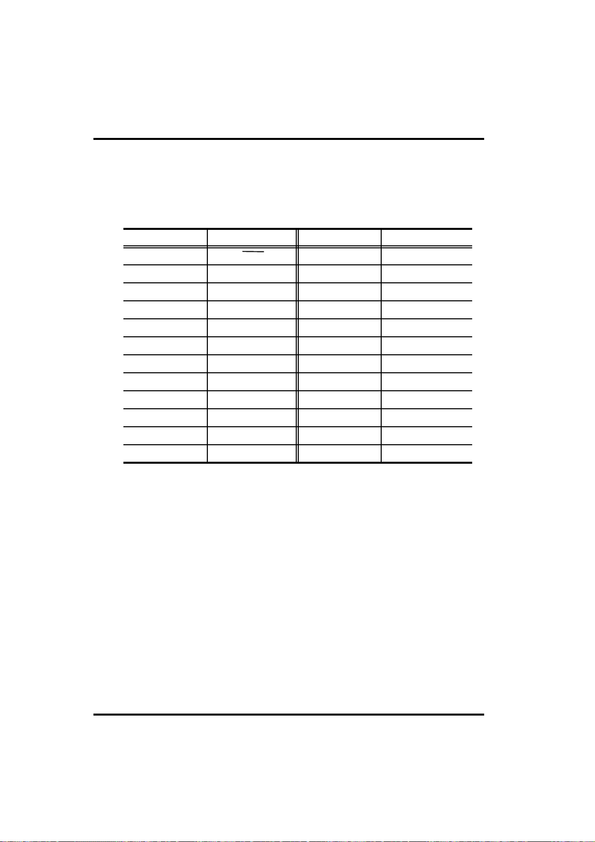
Connection
Perform emulation with the following connectors.
[User] Connection socket
The cable for the target system is connected.
Pin No.
1
2 GND 14 D1
3 R0 15 D2
4 R1 16 D3
5 R2 17 D4
6 R3 18 D5
7 K0 19 D6
8 K1 20 D7
9 K2 21 Remout
10 K3 22 OSC2
11 D0 23 OSC1
12 D8 24 VDD
Signal
Reset
Pin No.
13
Signal
D9
[M1] Monitor pin
Operations inside the GMS 30000 EVA can be monitored. Signals that can be
monitored are as follows.
AC0~AC3, X0, X1, Y0~Y3, REMDATA, CK2, CK5, WDTR, GND
[M2] Oscillation monitoring pin
The oscillation output signal can be monitored.
[T1] D8 output monitoring pin
The D8 output signal can be monitored.
[T2] D9 output monitoring pin
The D9 output signal can be monitored.
4 - 2
Page 50
Chapter 4. Evaluation Board
Optional setting
The following optional setting in accordance with the application system
specifications is required :
[S1] Optional mask setting
Optional masks available with GMS300 series units can be set by selecting
short posts.
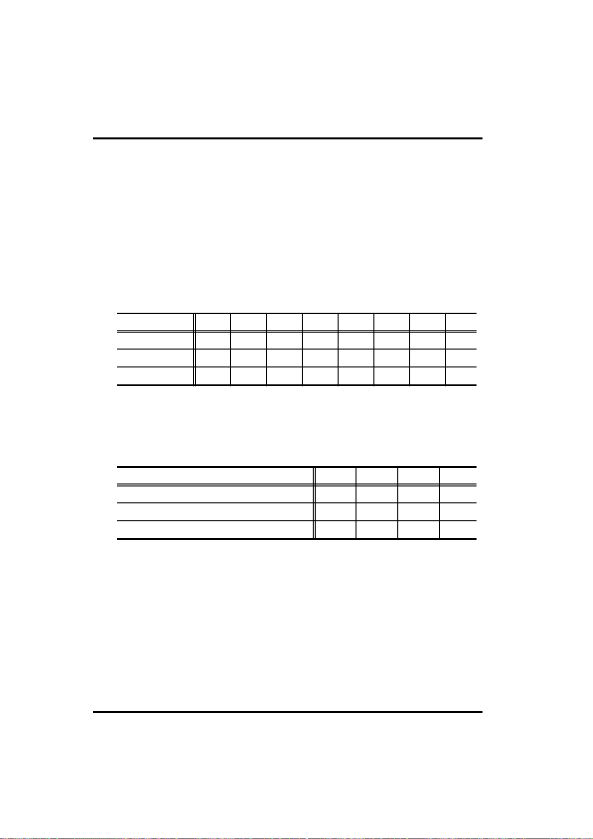
1. Setting of K-input and R-Port for STOP release
Shorting the KSR0 ~ KSR3 and RSR0 ~ RSR3 with the side of H can set the
STOP releasing function by the corresponding KSR0 ~ KSR3 and RSR0 ~
RSR3. If no STOP releasing function is desired, short them with the side of L.
Setting pin
Short post
Setting of STOP
No setting of STOP
K0
KSR0
H
L
K1
KSR1
H
L
K2
KSR2
H
L
K3
KSR3
H
L
R0
RSR0
H
L
R1
RSR1
H
L
R2
RSR2
H
L
2. Setting of pull-up resistor built-in R-Port pull-up resistor can be built in the
R-Port by shorting the corresponding RPU0 ~ RPU3 with the side of H.
If installation of built-in pull-up resistor is not desired, short them with the
side of L.
Setting pin
Short post
Built-in pull-up resistor installation
No built-in pull-up resistor installation
R0
RPU0
H
L
R1
RPU1
H
L
R2
RPU2
H
L
R3
RSR3
H
L
R3
RPU3
H
L
4 - 3
Page 51
Chapter 4. Evaluation Board
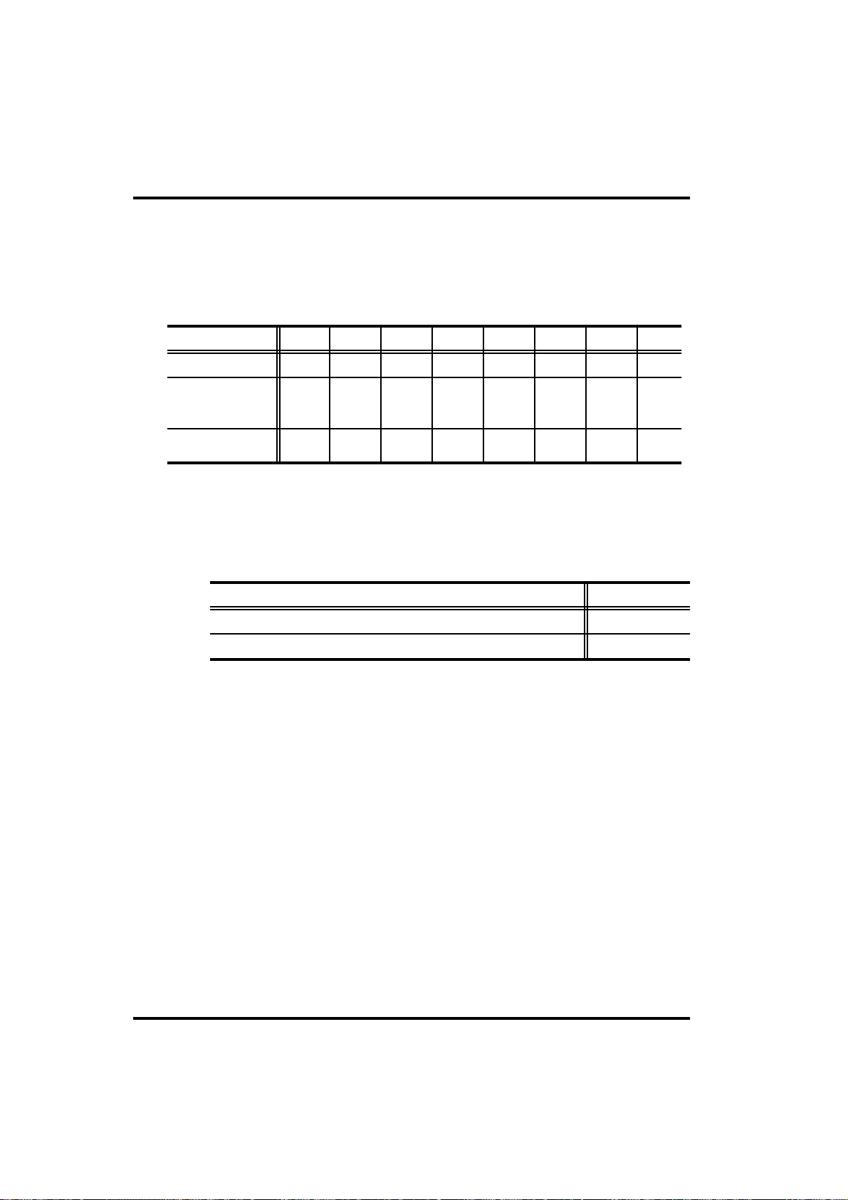
3. Setting of output condition of D0~D7 in STOP
Shorting the DSC0~DSC7 with the side of H can set the output condition of
corresponding D-output in STOP at ¡ÈL¡È forcibly.
To set the condition of usual output (the condition before STOP started is
maintained), short them with the side of L.
Setting pin
Short post
Forced setting at
¡ÈL¡È
in STOP
release
Usual output in
STOP released
D0
DSC0
H
L
D1
DSC1
H
L
D2
DSC2
H
L
D3
DSC3
H
L
D4
DSC4
H
L
D5
DSC5
H
L
DSC6
4. Setting of watch dog timer release with REMOUT output
The watch dog timer can be reset with REMOUT output signals by shorting
the WDTM with the side of L.
If the WDT resetting with REMOUT output signals is not desired, short it
with the side of H.
Short post
Reset timer
[S2] External STOP setting
STOP can be set from the outside by shorting the S2 toward the side of H.
Usually, short it toward the side of L.
D6
H
L
WDTM
D7
DSC7
H
L
L
HDo not reset timer
[S3] Power supply connection
This selection should be strapped to VDD.
4 - 4
Page 52
Chapter 4. Evaluation Board
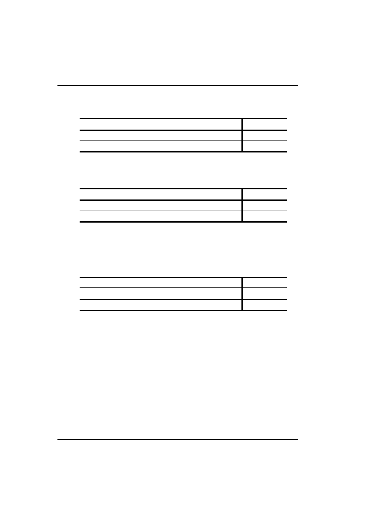
[S4] EPROM 2764/128, and 27256 can be installed by switching over the S4. For
EPROM, however, right-justify ROM chip pin 1 from socket pin 3.
Short post
2764/128
S4
H
L27256
[S5, S6] Clock input selection
Self-induced oscillation with the external clock input and oscillator can be set by
switching over the S5 & S6
Short post
External clock input
S5 & S6
U
XInternal self-induced oscillation
For internal clock input, install an oscillator on the PCB. Since the oscillation
circuit constant varies depending on the oscillator, adjust the constant by
referring to the oscillator manufacture`s recommendable values.
[S7, S8, JP] Clock input selection
MHz and KHz oscillation can be selected by switching over the S7, S8 and JP.
Short post
MHz oscillation
S7 & S8 & JP
M
4 - 5
KKHz oscillation
Page 53
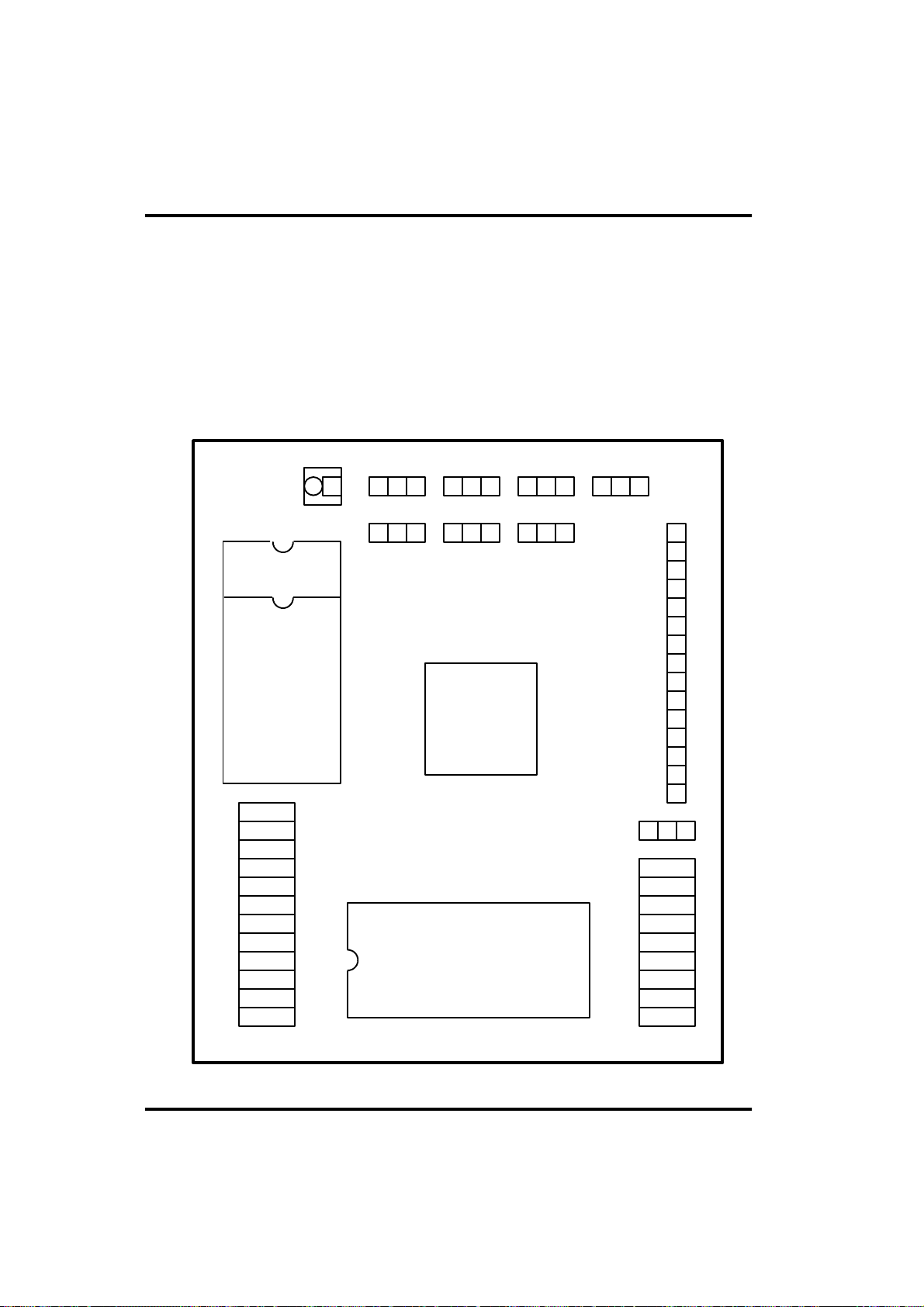
Chapter 4. Evaluation Board
Caution on Operation
• It is required to install a 24DIP IC socket in the application system. The
connection cable is connected to the socket.
• There is a possibility that the ceramic oscillator on the application system cannot
oscillate properly due to the influence of connection cable wiring capacitor or other
reasons. In such a case, install the oscillator on the evaluation board.
• Since the GMS 30000 EVA is designed to evaluate the program operations, there
is a case where the AC and DC characteristics differ from those of the mass produced chips
P1
1 28
Connector
H
RSR0
S1
RSR1
RSR2
RSR3
RPU0
RPU1
RPU2
RPU3
KSR0
KSR1
KSR2
KSR3
L
S3 S5 S6
H L U X U X M K
S4 S7 S8
H L M K M K
E V A
80
1
EPROM
(80QFP)
GSEN
EVA30000
GND
24
1
USER
Connector
(24Pin Socket)
T1
T2
JP
WDTR
REM DATA
S2
S1
WDTM
DSC7
DSC6
DSC5
DSC4
DSC3
DSC2
DSC1
DSC0
GND
CX3
CX2
X1
X0
AC3
AC2
AC1
AC0
Y3
Y2
Y1
Y0
H L
BKPOINT
H L
M1
Fig 4-1 Layout Diagram
4 - 6
Page 54
INTRODUCTION 1
ARCHITECTURE 2
INSTRUCTION 3
EVALUATION BOARD 4
SOFTWARE 5
APPENDIX 6
Page 55
CHAPTER 5. Software
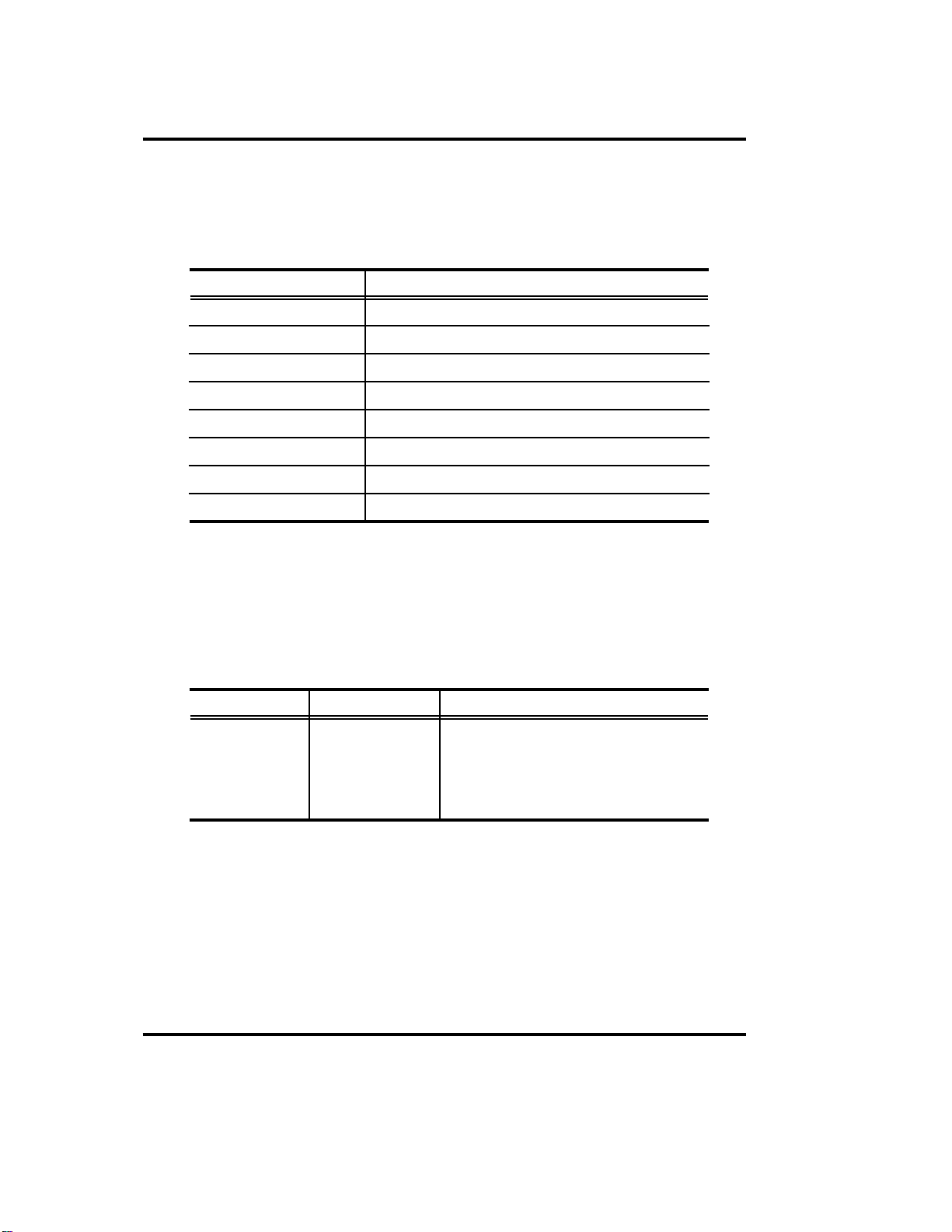
Configuration of Assembler
Chapter 5. Software
Execute File
GA80.EXE
GMSHEX.EXE Create HEX.file
GMSTST.EXE Create instruction check file
GS.BAT Batch processing of the above
Assembler
Create assembler list fileGMSLST.EXE
Create cross refere nce fileGMSCRF.EXE
Create ROM dump fileGMSROM.EXE
Instruction library fileGMS30K.LIB
Description
Boothing up Assembler
Creating your own source file with the extension name of SRC and execute batch
file (GS.BAT). This batch file converts the source code written in mnemonic into
machine language and generate a kind of useful file.
C> GS Source file (.SRC)
Input File
EX.SRC
Output File
EX.LST
EX.RHX
EX.CRF
EX.TST
EX.DMP
EX.SYM
List file
Hexa file (for EPROM, simulator)
Cross reference file
Instruction check file
ROM dump file (for masking data)
Symbol file
Content
* HEX and PRN file is intermediate file
5 - 1
Page 56

Chapter 5. Software
Configu r at io n of Sim ulator
1. Overvi ew
The simulator is a program for GMS300 Series 4-bit one-chip microcomputer.
The environment is organized based upon Hexa file of *.RHX and Cross Reference file
of *.CRF generated by assembling the source program coded by programmer.
Execution Environment
System : IBM-PC/AT or higher (MS-DOS or PC-DOS)
Video : Hercules, EGA or VGA color
Organizing files
GSSIM.EXE : Simulator execution file
GMS30K.GSP : Store the simulator environment. It is
generated automatically when executing
the program initially (Selected CPU.
Store the file names previously loaded.).
GMS30K.HLP : Help file of simulator commands.
GMS30K.LOG : Record the working history of users. Generated
by LOG ON and LOG OFF commands.
*.BAT : List a set of simulator command. Generated by
user.
PORTIN.DAT : Provide the port input-value when executing
the simulator. Generated by user.
Supporting CPU
GMS30004, GMS30012, GMS30112, GMS30120, GMS30140
5 - 2
Page 57

Chapter 5. Software
2. Characteristics of Simulator
- User-friendly pop-up window menu. Select the necessary command and display
the screen in windows format so that users can know the execution results.
- Display always the register window in the right side so that programmer can check
easily the change of data memory value as program proceeds.
- Maintain the previous simulator environment if user does not make the extra changes
when re-executing after logging out completely from the simulator
previously executed by loading the source program. In other words, the previously-
executed file is automatically loaded when the simulator is executed (GMS30K.GSP
file).
- When trace command ([F8] or > T command) is executed, the changed values are
noticed easily by displaying the highlighted changed values in register and memory
windows, if the contents of each register or data memory is changed as command
line is processed.
- When trace command ([F8] or > T command) is executed, the current execution
line is highlighted.
- Out of the simulator commands, load or save commands is executable in pop-up
windows. In-line command is executable as prompt command in the command
window.
5 - 3
Page 58

Chapter 5. Software
3. Screen Or ga ni zation of Simu lator
Screen is basically organized with four windows; Memory, Source, Command and
Register. Source and Command windows can be enlarged up to the full screen
size (CTRL-[F10]). Movement between windows is made by [F6].
3.1 Memory Window
Data memory contents of the currently selected micom is displayed. 32 nibble
data values of 00~1F(h) addresses are displayed.
3.2 Source Window
The contents of *.RHX file called by load command is displayed in the state of
being disassembled. Addresses are displayed randomly in the state of
polynomial together with instruction code and mnemonic. If *.CRF file is
called, label is displayed at the corresponding position. Display position of
source program is adjustable with Up/Down arrow keys and Page Up/Down
keys.
3.3 Command Window
All kinds of commands provided by simulator is executed by In-line command,
and the execution results of the commands are displayed. Command window
size is adjustable with [CTRL]-[F10].
5 - 4
Page 59

Chapter 5. Software
3.4 Register Window
Display each register value inside micom, I/O port value and machine cycle
altogether. When trace command is executed by function key [F8], the
register value after the previous command before the current program counter
is executed is displayed. All kinds of register and I/O ports displayed in
register window are as follows.
PC : Progr am counter 2digit 6bit [He xa ]
ACC : Accumula to r 1digit 4bit [Hexa ]
PA : Page add ress 1digit 4bit [He xa ]
PB : Page buf fer 1digit 4bit [He xa ]
X : X register 1digit 1 or 2 [Hexa]
Y : Y register 1digit 4 bit [Hexa]
ST : Status register 1digit 1bit [Binary]
PMR : Pulse mode register 1digit [Hexa]
WDT : Watch dog timer 1digit 14bit {Hexa]
SP : Stack pointer level 1digit
SR0 : Stack level 0 4digit
SR1 : Stack level 1 4digit
SR2 : Stack level 2 4digit
OUT : Remocon out output [Binary]
K : K port input register 4bit [Binary]
Rin : R port input register [Binary]
Rout : R port output register [Binary]
D : output port 6or8 10bit [Binary]
Machine Cycle :
The number of command execution is displayed in decimal.
5 - 5
Page 60

Chapter 5. Software
4. Comma nd s in Eac h Me nu
^stands for [CTRL] key, while @ stands for [ALT] key.
4.1 File Menu
Use the function key behind each command as a hot key or execute each
com m and through selecting [ALT]-[F ] key and pressing the highlighted
character.
Load RHX F2 : Load the file named *.RHX, analyze the selected Hexa file
and disassemble it. Display the program address, assemble
code and mnemonic. The order of displayed program
addresses follows the POLYNOMIAL form. Even when the
extention is not input in case of selection, .RHX extension is
presumed to include.
Load CRF @F2 : If Cross reference file of loaded file loads the *.CRF file,
labels and variables assigned by programmer are displayed
at accurate position of Source window so that programmer
can read the program easily. Even when the extension is not
input in case of file selection, .CRF extension is presumed to
include.
Write RHX F3 : When any modifications are made to source program or
program memory after the simulator is loaded once, the
modifications are stored in the same or new filename as
loaded. It has the same command and function as > WP
[filename] of In-line command.
Log ON/OFF F4 : After the simulator is executed, all the input and results are
stored in the filename GMS30K.LOG Once function key [F4]
is pressed, log-in starts, and if the key is pressed one more
time, log-in file is closed in a toggling way. The ON/OFF
state of log-in is displayed in the upper-right corner. It has
the same function as > LOGON and > LOGOFF of In-line
commands.
Os shell @S : When users want to work temporarily under DOS environment,
this command is used. When users want to back to Windows
environment, input > EXIT.
Exit @X : Used when getting completely out of the simulator environment.
5 - 6
Page 61

Chapter 5. Software
4.2 Window Menu
Use the function key behind each command as a hot key or execute each
com m and through selecting [ALT]-[W ] key and pressing the highlighted
character. Function key [F6] provides the return function to each window.
Command Box: Position the cursor in command window to make it possible to
use In-line command provided by the simulator.
Source Box : Position the cursor in source window to make it possible for
programmer to see the disassembled source program. It is
possible to use Up/Down arrow keys and Page Up/Down
keys.
Zoom ^F10 : Position the cursor in command or source window, and then
select Zoom or press [CTRL]-[F10] key to enlarge the window
to the full screen size.
5 - 7
Page 62

Chapter 5. Software
4.3 Run Menu
Use the function key behind each command as a hot key or execute each
com m and through selecting [ALT]-[R] key and pressing the highlighted
character.
MCU Reset ^F9 : Initialize the execution environment of the simulator. In
other words, initialize the register value to 0 or 1, and
machine cycle value is changed to 0. It has the same
command and function as > CR command of In-line
command.
Go F5 : Program executes from the current value of program counter.
Press [ESC], [Enter] or [Space] key to stop execution, and
display the current register value.
Animate @5 : Program executes from the current value of program counter.
The value of data memory or registers are highlighted in the
corresponding window. Press [ESC], [Enter] or [Space] key to
stop execution. Because of speed difference among system,
the speed is adjustable from 0 to 40.
(0 : fastest, 40 : slowest)
Trace F8 : Program executes line by line from the current value of
program counter. The changing values of registers and
memory are highlighted in register window and memory window
respectively.
Execute Batch : When the batch filename consisted of a set of commands
made by user using editor is input, each command executes
automatically as In-line command is input. It has the same
function as > BAT command of In-line command.
5 - 8
Page 63

Chapter 5. Software
4.4 Option Menu
T o execute each command, select [ALT]-[O] key and press the highlighted
character in each command line. Or select the menu and press the [Enter]
key.
MCU Select : Select according to the kind of micom. Able to select on of
GMS30004, 30012, 30112, 30120 or 30140 among GMS300
series. Once the command is executed, the window
indicating the characteristics of each micom is open. Press
Left, Right, Up Down key to select the micom to work.
Setup : Set the execution mode of selected micom. It has the same
function as > SET command of In-line command. Once the
function is executed, a small <Setup> window is open.
Position the cursor in either of I/O Input and Output mode,
Symbol, Execution Mode of Watch Dog Timer with the item to
change. Assign the corresponding execution mode with Left,
Right arrow key.
Execution Mode to be Assigned in <Setup>
I/O Input [pi] = [0] Port Input from I/O register
[1] Port input from keyboard
[2] Port input from file (PORTIN.DAT)
I/O Output = [0] No display
[1] Display
[2] Display & Break
Symbol = [0] Search
[1] Unsearch
Watch Dog Timer = [0] OFF
[1] ON (No option)
[2] ON (Option)
5 - 9
Page 64
Chapter 5. Software
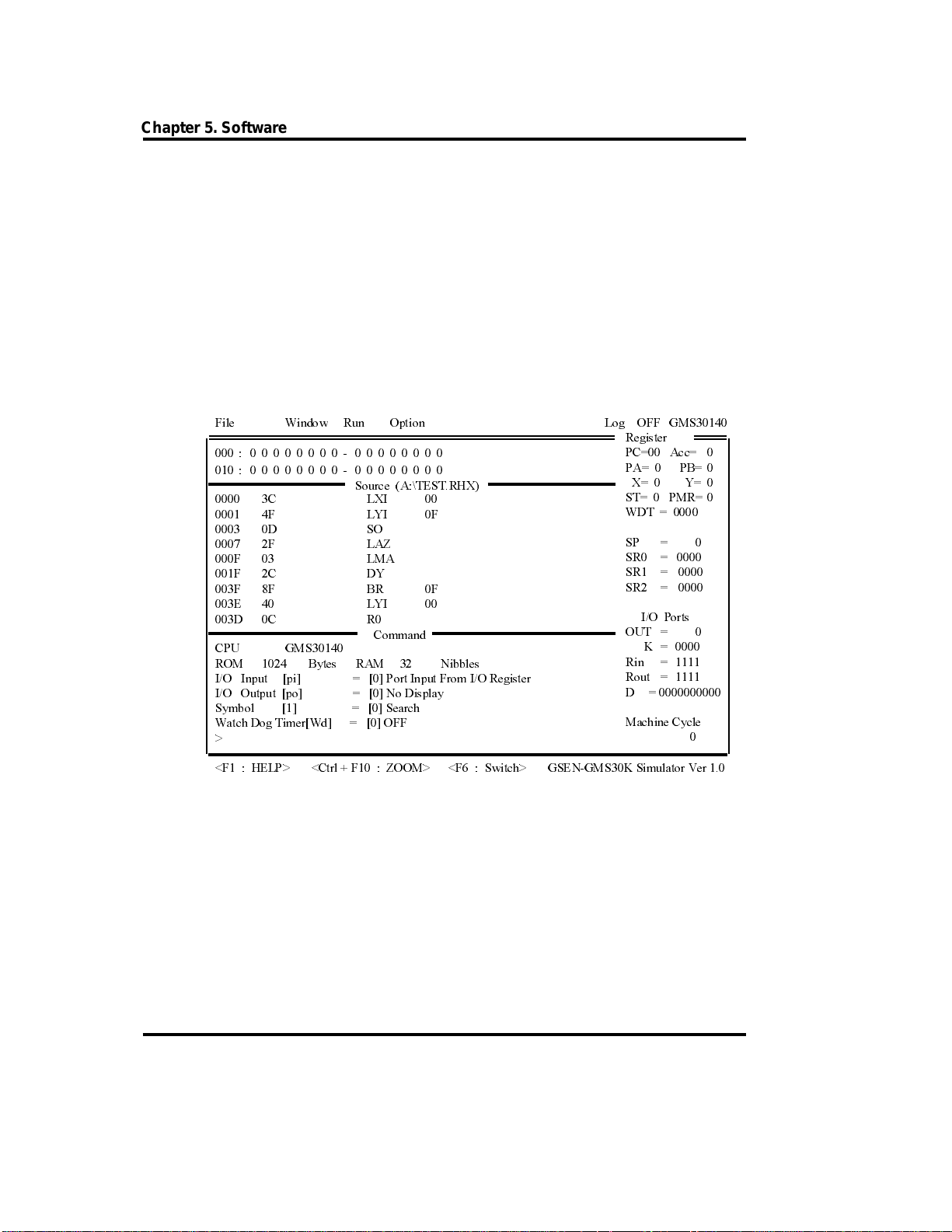
5. Simulator Execution
5.1 File Load
Use one of three ways to load the file to run from the simulator. First execute
the GSSIM.EXE file from DOS and name it as a parameter.
>a:\GSSIM TEST.RHX (Here the extention needs not be input.)
The following screen will be displayed.
)LOH :LQGRZ 5XQ 2SWLRQ /RJ 2)) *06
6RXUFH $?7(675+;
& /;,
) /<, )
' 62
) /$=
) /0$
) & '<
) ) %5 )
( /<,
' & 5
&RPPDQG
&38 *06
520 %\WHV 5$0 1LEEOHV
,2 ,QSXW >SL@ >@ 3RUW ,QSXW )URP ,25HJLVWHU
,2 2XWSXW >SR@ >@ 1R 'LVSOD\
6\PERO >@ >@ 6HDUFK
:DWFK 'RJ 7LPHU>:G@ >@ 2))
!
) +(/3! &WUO ) =220! ) 6ZLWFK! *6(1*06. 6LPXODWRU 9HU
5HJLVWHU
3& $FF
3$ 3%
; <
67 305
:'7
63
65
65
65
,2 3RUWV
287
.
5LQ
5RXW
'
0DFKLQH &\FOH
5 - 10
Page 65

Chapter 5. Software
Second, execute the GSSIM.EXE file and then the Load RHX (Hot key is
[F2]). The following small window is open at the center of screen waiting for
user to input the Hexa filename to work.
* File Name *
A : \UNNAMED .R HX
When no file is selected, Unnamed.rhx filename is displayed. When the
filename to work is input immediately, the file from the current directory is
called. If the specific directory is assigned, the file from the assigned directory
is called.
Third, call the file to work through using the >LP [filename] from command
window by in-line command.
Here for example, load the TEST.RHX file
* File Name *
A : \TEST.RH X
TEST.RHX file is called and the contents of HEXA file is analyzed from the
simulator. The source contents in the state of being disassembled is
displayed from Source window. Incase of filename input, although RHX is not
input, .RHX extension presumed to include by default.
5 - 11
Page 66
Chapter 5. Software
Also when there is Cross Reference File of working file, press Load CRF (Hot
key [ALT]-[F2]). The following small window is open at the center of screen
waiting for user to input *.CRF filename.
* File Name *
A : \TEST.CR F
The filename called by Load RHX command is displayed by default as .CRF
filename. When .CRF file is called, the label of source program created by
programmer is displayed at the label position of Source window for easy
reading of program by user.
5 - 12
Page 67

Chapter 5. Software
5.2 File Store
When the specific part of source program is changed under the simulator
environment by calling the working file, the corresponding Hexa file needs to
be stored. Use one of the following two methods.
First, when executing the pop-up command Save RHX (Hot key is [F3]), the
following small window is open at the center of screen waiting for user to input
the Hexa filename. The filename called by file load command by default is
displayed. When the filename is not changed, hit just the [Enter] key. When
user wants to change the filename to store, input the filename to change.
* File Name *
A : \TEST.RH X
Second, store the processed Hexa file using > WP [filename] from command
window with In-line command.
Ì
Here when the same filename to store already exists in the disk,
File
Already ExistÌ message comes up asking user by [YES/NO] if user overwrite
or not.
5 - 13
Page 68
Chapter 5. Software
5.3 Clo sin g the Simulator
Using the pop-up command Exit (Hot key [ALT]-[X]) or In-line command > Q,
exit from the simulator environment.
When execute the command, the following message comes up for the check-
up asking the user`s intention to store, if user does not store the changed file
after changing the loaded file to work. Use Tab key or left, right direction key
to select YES/NO.
Program have changed. Save it ?
Yes No
Als o for r ecording the work contents, even when exiting the simulator without
Log OFF, Log OFF is done automatically and GMS30K.LOG file is stored.
5 - 14
Page 69

6. Simulator Commands
6.1 Command Syntax
1) A (Assemble)
To assemble what is commanded for every line from the specified
<address> and write in the memory.
2) BAT (Batch)
To execute what is commanded in the command file in a batch.
When there is a format error, command error is issued and execution is
stopped at the error point.
3) BP (Break Point set), BL (Break point List)
To set break point.
To display the set break Point.
4) BS (Break point set step)
To set break point with No. of steps.
Chapter 5. Software
5) BC (Break point Clear)
To clear the specified No. break point.
6) CR (CPU Reset)
To reset the simulator to the initial state.
7) DPP (Dump Program memory)
To display the content of the memory in the area of the No. of pages
specified with <In> from the specified <address> in hexadecimal. The
address here is polynomial.
8) DPS (Dump Program memory)
To display the content of the memory in the area of the No. of pages
specified with <In> from the specified <address> in hexadecimal.
9) DD (Dump Data memory)
To display all the data in Data Memory in hexadecimal.
10) EPP (Exchange Program memory)
To display and modify the specified data in the program memory.
Address here is polynomial.
5 - 15
Page 70

Chapter 5. Software
11) EPS (Exchange Program memory)
To display and modify the specified data in the program memory.
12) ED (Exchan ge Data memo ry)
To display or modify data in the specified data memory.
13) FPP (Fill Program memory)
To fill the area of the program memory specified with <In> from the specified
<address> with the specified byte data. The address here is polynomial.
14) FPS (Fill Program memory)
To fill the area of the program memory specified with <In> from the specified
<address> with the specified byte data.
15) FD (Fill Data memory)
To fill the area of the data memory specified with <In> from the specified
<address> with the specified nibble data.
16) G (Go)
To execute the program in the specified program memory.
17) H (Hex calculate)
To add or subtract in hexadecimal.
18) LOGON (LOGIN)
To log the commands executed after this command.
19) LOGOFF (LOGOUT)
To end logging.
20) LP (Load Program from MS-DOS* file)
To load `files` on MS-DOS* to the memory.
21) MPP ( Move Program memo ry)
To transfer data in the memory area to another area.
The address here is polynomial.
5 - 16
Page 71

22) MPS (Move Program memory)
To transfer data in the memory area to another area.
23) P (Port set)
To set the specified data at the specified I/O register.
24) Q (Quit)
To return to MS-DOS*.
25) R (Register dump or change)
To display or modify the register data.
26) SET (setup )
To set the operation Mode for the simulator.
27) SL (Symbol file Load)
To load symbol tables from the specified symbol file.
28) ST (Status)
To display the simulator status.
Chapter 5. Software
29) T (Trace)
To execute the program in the specified program memory address a single step.
30) TMT (Ti m e )
To obtain time from the No. of machine cycles and clock frequency.
31) TMC (Time)
To obtain No. of machine cycle from the time and clock frequency.
32) U (Unassemble)
To unassemble data in the area specified with <In> from the specified <address>
and display in mnemonic.
33) Wp (Write Program to MS-DOS* file)
To read-out data in all the ROM area and write the Intel hexa data in the files
specified with <file name>.
34) ? (Help)
To display the list of commands of this simulator
5 - 17
Page 72

Chapter 5. Software
6.3 Description of Commands
The symbols used in this chapter are defined as in below.
1) XXXX Indicates input from the keyboard.
2)
ã
Indicates Return key.
3) _ Indicates insertion of space characters.
4) In Indicates range.
5) [ ] Indicates it is omittable.
6) No. used on this system are hexadecimal. However, the machine cycles are
decimal.
(Common items on this simulator)
1) This simulator accepts up to 132 characters per each line.
Before pressing `ã` key, data can be modified in the following procedure.
<BS> Key deletes one character and the cursor sets back by one character.
2) Commands can be input both in block and small letters and both are treated
as the same.
3) Commands can be terminated by inputting `.`.
4) Command history (recall)
This simulator has 16 command buffers and each time `Control A` is
pressed, command immediately before the current one is displayed.
5) When `!XX` is executed to `*`, MS-DOS* commands can be executed
temporarily.
6) Regarding the omission indicated with [ ], when one [<address>] or [In] is
omitted, the area may not be recognized. In this case, be careful as the
current operation cannot be ensured.
7) When `.XXXX` is specified, it is treated as a symbol. Therefore, before using
this specification, specification of Symbol file should have been made.
8) When `ESC` key is pressed, command execution is stopped and the system
moves to `*` mode.
9) When In is LXX< XX indicates No. of words and when there is no L, XX
indicates an address.
10) For command separator (indicated with_in this Manual), `_` or `,` can be
used.
11) When `Control C` is pressed, the system goes back to `MS-DOS*`.
12) In case of both sequential and polynomial address, the first two digits of an
<address> indicate No. of page and the latter two digits indicate the address.
Hereunder is the explanation on each command used on this system.
5 - 18
Page 73

Chapter 5. Software
A (Assemble)
[Function]
To assemble commands for each line from the specified <address> and write
them in the memory.
[Format]
> A_ [<address>]
[Explanation]
With this, the system assembles commands for each line from the specified
<address> and writes them in the memory.
When <address> is omitted, data is written from the current `PC` address.
Assemble can be finished by keying in `.`.
When `_` is keyed in, the system goes back the address just before the current
one.
[e.g.]
>A 200
0200 40 LYI 0
0201 21 LAM
0203 77 ALEI 14
0201 03 LMA
0200 0D SO
>
ã
ã
ã
ã
SO
ã
ã
LMA
ã
ã
-
ã
ã
-
ã
ã
.
ã
BAT (Batch)
[Function]
To execute commands in the command file in a batch. When there is a format
error, execution is stopped there and command error is issued.
[Format]
BAT_<File Name>
[Explanation]
With this command, the system executes commands in the command file in a
batch. When there is a format error, execution is stopped there and command
error is issued. In order to execute this command, it is required to create the
command file on the editor in advance.
[e.g]
>BAT test.bat
>R PA 0
>R PB 0BATCH END
>
ã
ã
ã
5 - 19
Page 74

Chapter 5. Software
BP (Break Point set), BL (Break point List)
[Function]
BP To set the break point.
BL To display the set break point
BPS To set step break point.
[Format]
BP[n]_adr[_m]
n : Set break No. 0~9.
adr : Set address for setting break
m : Valid only when n=0, setting No. of times to pass the break
BPS_st
ã
st : Set No. of steps.
BPI
ã
BPO
ã
BL
ã
ã
point. The m range is 1
õmõ
hexadecimal.
st range is 1õstõ2147483647.
st value should be set in decimal.
255. m value should be set in
[Explanation]
This command is used to the break point.
Break on this simulator is to stop after executing the command on the specified
address.
When `BPS st` is specified, the system stops when the value on the machine
cycle register becomes equal to st.
When `BPI` is specified, the system stops before command execution every time
command input is made.
Unassemble displayed in this case is the address with input command.
When `BPO` is specified, the system displays the value on that occasion on CRT
and stops every time output command is made.
When `BP` only or `BL` is specified, the state of the currently set break point is
displayed.
It is possible to used symbols for specifying adr.
When `n` is omitted in break setting command, No. shall be allocated from 1 to all
empty No.
5 - 20
Page 75
Chapter 5. Software
[e.g .]
1) Example to occur break after passing page 1 address 0 three times.
>BP0 100 3
ã
ã
2) Example to set a break point at page 5 address 0.
>BP 500
ã
>BL
ã
0 = 0100 ( 3)
1 = 0500
ã
ã
3) Example to occur break on the main label (in case the main label is at page 5
address 0.)
>BP .main
>BL
ã
ã
0 = 0100 ( 3)
1 = 0500 .MAIN
>
ã
ã
4) Example to occur break by No. of steps (50 steps).
>BPS 50
>BL
0 = 0100 ( 3)
1 = 0500 .MAIN
S50
>
ã
ã
ã
ã
5) Example to occur break with input command.
ã
>BPI
ã
>G
ã
ã
RUN
******** MC Step Break ********
0004 00 NOP
PC=00 PA=09 PB=00 A=0 X=0 Y=0 ST=1 PMR=0 WD=0000 MC=50
>R R 00
>G
ã
ã
ã
ã
6) Example to occur break with output command.
>BP0
>G
RUN
Rout=1111 D=11111111 OUT=0 MC=125
******** Break AT Port Out !! ********
002F 0D SO
PC=00 PA=1E PB=00 A=0 X=0 Y=F ST=1 PMR=0 WD=0000 MC=125
>G
ã
ã
ã
ã
ã
ã
5 - 21
Page 76

Chapter 5. Software
BC (Break Point Clear)
[Function]
To clear the break point at the specified No.
[Format]
ã
BC_n
[Explanation]
With this, the system clear the break point at the specified No.
When n is omitted, the state of the currently set break shall be displayed.
When n is `*`, all the break points shall be cleared.
[e.g]
ã
>BL
ã
0 = 0100 ( 3)
1 = 0200
2 = 0500
S 50
I
O
>BC 1
>BC S
>BC I
>BC O
>BC
0 = 0100 ( 3)
2 = 0500
>BC *
>BL
>
ã
ã
ã
ã
ã
ã
ã
ã
ã
ã
ã
ã
ã
ã
5 - 22
Page 77

Chapter 5. Software
CR (CPU Reset)
[Function]
To set simulator to the initial state.
[Format]
ã
CR
[Explanation]
When this command is executed, the simulator is set back to the initial state. In
this case, the registers are also initialized according to each CPU. However, MC
is cleared irregardless of the CPU status.
Initial State of each register.
PA, PC, PB, SP and D PORT become 0.
All the ports of R PORT become 1.
The other registers are undefined.
[e.g]
ã
>CR
ã
CPU GMS30140
ROM 1024 Byte RAM 32 Nibble
I/O Input [pi] = [0] Port input I/O register
I/O Output [po] = [0] No Display
SYMBOL [1] = [0] Search
Watch Dog Timer [wd] = [0] off
PC=00 PA=00 PB=00 A=0 X=0 Y=0 ST=0 PMR=0 WD=0000 MC=0
SP=0 SR1=0000 SR2=0000 SR3=0000
I/O Reg. Rin=1111 Rout=1111 D=00000000 OUT=0 K=0000(0h)
>
5 - 23
Page 78

Chapter 5. Software
DPP (Dump Program memory)
[Function]
To display data in the program memory area specified with <In> from the
specified <address> in hexadecimal.
[Format]
DPP_[<address>_<In>]
ã
[Explanation]
When this the system displays data in the program memory area specified with
<In> from the specified <address> in hexadecimal. When [ ] is omitted, 64 bytes
of data from the succeeding address shall be displayed. The address used with
this command is polynomial.
[e.g]
>DPP 0 20
0000 : 00 01 02 03 04 05 06 07 - 08 09 0A 0B 0C 0D 0E 0F
0027 : 10 11 12 13 14 15 16 17 - 18 19 1A 1B 1C 1D 1E 1F
001C : 20 21 22 23 24 25 26 27 - 28 29 2A 2B 2C 2D 2E 2F
0022 : 31 32 33 33 34 35 36 37 - 38 39 3A 3B 3C 3E 3E 3F
>
ã
ã
DPS (Dump Program memory)
[Function]
To display data in the program memory area specified with <In> from the
specified <address> in hexadecimal.
[Format]
DPS_[<address>_<In>]
ã
[Explanation]
When this the system displays data in the program memory area specified with
<In> from the specified <address> in hexadecimal. When [ ] is omitted, 64 bytes
of data from the succeeding address shall be displayed. The address used with
this command is sequential.
[e.g]
>DPS_0_3F
0000 : 00 01 03 07 0F 1F 3F E3 - 3D 3B 37 2F 1E 3C 39 33
0010 : 27 0E 1D 3A 35 2B 16 2C - 18 30 21 02 05 0B 17 2E
0020 : 1C 38 31 23 06 0D 1B 36 - 2D 1A 34 29 12 24 08 11
0030 : 22 04 09 13 26 0C 19 32 - 25 0A 15 2A 14 28 10 20
>
ã
ã
5 - 24
Page 79
Chapter 5. Software
DD (Dump Data memory)
[Function]
To display data in the data memory in hexadecimal.
[Format]
ã
DD
[Explanation]
With this, the system displays all the data in the data memory in hexadecimal.
[e.g]
ã
>DD
ã
000 : 6 C 6 0 0 0 0 0 - 0 0 0 0 0 0 0 0
010 : 1 2 3 4 0 0 0 0 - 3 2 1 0 0 1 0 1
>
ED (Exchange Data memory)
[Function]
To display and modify the specified data memory.
[Format]
ED_[<address>
ã
[Explanation]
When this the system displays and modifies the specified data memory. This
Mode is continuous and processing shall be continued until *.* is pressed. When
`_` is pressed, the system goes back to the address immediately before.
[e.g]
>ED 0
00 : 7 >
01 : 6 >
02 : 7 >
>
ã
ã
ã
3
ã
ã
6
ã
ã
.
ã
5 - 25
Page 80

Chapter 5. Software
EPP (Exchange Program memory)
[Function]
To display and modify the specified program memory.
[Format]
EPP_<Addre ss>
ã
[Explanation]
With this, the system displays and modifies the specified program memory. This
mode is continuous and each time `ã` is pressed, the succeeding address shall
be displayed, setting operation shall be performed continuously until `.` is
pressed. When `_` is pressed, the system goes back to the address immediately
before. The address used with this command is polynomial. It is possible to use
symbols in <address>.
[e.g]
>EPP_100
100 : 0D>37
101 : 77>AF
103 : 42> .
>
ã
ã
ã
ã
ã
ã
ã
ã
EPS (Exchange Program memory)
[Function]
To display and modify the specified data memory.
[Format]
EPS_<Address>
ã
[Explanation]
With this, the system displays and modifies the specified program memory. This
Mode is continuous and each time `ã` is pressed, the succeeding address shall
be displayed and setting operation shall be performed continuously until `.` is
pressed. When `_` is pressed, the system goes back to the address immediately
before. The address used with this command is sequential.
It is possible to use symbols in <address>.
[e.g]
>EPS_100
100 : 48>6
101 : 04>45
102 : 53>.
>
ã
ã
ã
ã
ã
ã
ã
ã
5 - 26
Page 81

Chapter 5. Software
FPP (Fill Program memory)
[Function]
To fill the program memory area specified with <In> from the specified <address>
with 1 byte data.
[Format]
FPP_<Address>_<In>_<Data>
ã
[Explanation]
With this, the system fills the program memory area specified with <In> from the
specified <address> with 1 byte data. It is possible to use symbols in <address>.
[e.g]
>FPP 100 L10 55
>DPP 100
0100 : 55 55 55 55 55 55 55 55 - 55 55 55 55 55 55 55 55
0127 : 10 11 12 13 14 15 16 17 - 18 19 1A 1B 1C 1D 1E 1F
011C : 20 21 23 24 25 26 27 29 - 29 2A 2B 2C 2D 2E 2F 30
0122 : 31 32 33 34 35 36 37 38 - 39 3A 3B 3C 3D 3E 3F 40
>
ã
ã
ã
ã
FPS (Fill Program memory)
[Function]
To fill the program memory area specified with <In> from the specified <address>
with 1 byte data.
[Format]
FPS_<Address>_<In>_<Data>
ã
[Explanation]
With this, the system fills the program memory area specified with <In> from the
specified <address> with 1 byte data.
It is possible to use symbols in <address>.
[e.g]
>FPS 100 L10 55
>DPS 100
0100 : 55 55 55 55 55 55 55 55 - 55 55 55 55 55 55 55 55
0110 : 01 00 11 01 01 20 00 00 - 01 00 00 0C 01 00 55 55
0120 : 01 00 11 01 01 20 00 00 - 01 00 00 0C 01 00 00 55
0130 : 01 00 11 35 01 20 00 55 - 01 55 00 55 55 55 55 55
>
ã
ã
ã
ã
5 -27
Page 82

Chapter 5. Software
FD (Fill Data memory)
[Function]
To fill the program memory area specified with <In> from the specified <address>
with one specified nibble data.
[Format]
FD_<Address>_<In>_<Data>
[Explanation]
With this, the system fills the data memory area specified with <In> from the
specified <address> with one specified nibble data. It is possible to use symbols
in <address>.
[e.g]
>FD 0 L3 4
ã
>DD
ã
000 : 4 4 4 0 0 0 0 0 - 0 0 0 0 0 0 0 0
010 : 0 0 0 0 0 0 0 0 - 0 0 0 0 0 0 0 0
>
ã
ã
ã
5 - 28
Page 83

Chapter 5. Software
G (Go)
[Function]
To execute the program in the specified program memory
[Format]
G_[<Address 1>][_<Address 2>].. .[ _<A ddress 8>]
[Explanation]
With this, the system executes the program address specified with =, [=<address
1>] is omittable. When omitted, the command is executed from the present `PC`
address. The system also sets a break point in the specified address after
[_<address2>] . When `g` command is executed, simulation is started after
outputting `RUN` message. When any key is pressed in this state, simulation is
stopped.
It is possible to use symbols in the <address>.
[e.g]
ã
>G
1)
ã
RUN
******** User Break Point !! ********
010E 20 LMAIY
PC=01 PA=1D PB=01 A=7 X=1 Y=8 ST=1 PMR=0 WD=0000 MC=297
>
ã
>G=.STAR T 37 3
2)
******** Go Break Point !! ********
0003 BF BR 3F
PC=00 PA=07 PB=06 A=F X=3 Y=5 ST=1 PMR=0 WD=0000 MC=808
>
ã
ã
5 - 29
Page 84

Chapter 5. Software
H (Hex calculate)
[Function]
To add and subtract hexadecimal No.
[Format]
H_XXXX_ XXXX
ã
[Explanation]
Hexadecimal Nos. are added or subtracted.
[e.g]
>H_e6ab _b7fc
9ea7 2eaf
>
ã
ã
LOGON (LOGIN)
[Function]
To log the commands executed after this command.
[Format]
LOGON
[Explanation]
After executing this command, all the information displayed on CRT shall be
written consecutively until LOGOFF command is given. The file created in this
event is
ã
Ì
LOG.DAT`.
[e.g]
>LOGON
>
ã
ã
5 - 30
Page 85
Chapter 5. Software
LOGOFF (LOGOUT)
[Function]
To end logging
[Format]
LOGOFF
ã
[Explanation]
Logging is finished when this command is executed.
[e.g]
>LOGOFF
>
ã
ã
LP (Load Program from MS-DOS* file)
[Function]
To read `file` on MS-DOS* and write it to the program memory of the simulator
[Format]
LP_<file name>
[Explanation]
The system reads the file specified with <file name. RHX> and writes the data to
the address specified with <address>.
The file format is the Intel hexa format.
ã
[e.g]
>LP TEST. RHX
. . . . . . . . . . . . . . . . . . . . . . . . . .
. . . .
Program load OK!
>
ã
ã
5 - 31
Page 86

Chapter 5. Software
MPP (Move Program memory)
[Function]
To transfer memory area data to other area.
[Format]
MPP_<address_s>_<In>_<address_d>
ã
[Explanation]
With this command, the system transfers data upto the No. of words specified
with <In> from the address specified with <address_s> to the area specified with
<address_d>.
The address used with this command is polynomial.
[e.g]
>MPP 100 200 300
>
ã
ã
MPS (Move Program memory)
[Function]
To transfer memory area data to other area.
[Format]
MPS_<address_s>_<In>_<address_d>
ã
[Explanation]
With this command, the system transfers data upto the No. of words specified
with <In> from the address specified with <address_s> to the area specified with
<address_d>.
The address used with this command is sequential.
[e.g]
>MPS 100 200 300
>
ã
ã
5 - 32
Page 87
Chapter 5. Software
P (Port Set)
[Function]
To display and modify the specified I/O set registers.
[Format]
P_aa_bb_cã (When setting R, D port)
aa : I/O set register name
bb : Specify in or out
c : Set value (0 or 1)
P_aa_cc ã / P_aa_cã (when setting K)
aa : I/O set register name
bb : set value (one digit of a hexadecimal No.)
c : Set value (0 or 1)
[Explanation]
The system sets the value in the specified I/O set register.
[e.g]
Example of setting K
1)
> P K 8
ã
> P
ã
I/O Regs. Rin=0000 Rout=1111 D=00000000 OUT=0 K=1000(8h)
>
ã
ã
2) Example of K0-K3 setting
> P OUT 1
> P K1 1
ã
> P
ã
I/O Regs. Rin=0000 Rout=1111 D=00000000 OUT=1 K=0010(2h)
>
ã
ã
ã
ã
(I/O setting registers used on this simulator)
• Dout (D port output register 6 or 8 or 10bit)
• K (K input register 4bit)
• Rout (R port output register 4bit)
• Rin (R port input register 4bit)
• OUT (OUT port output register 10bit(
5 - 33
Page 88

Chapter 5. Software
Q (Quit)
[Function]
To return to PC-DOS
[Format]
ã
Q
[Explanation]
When this command is executed on the system with prompt (*display) waiting for
a command, the system moves from `simulator` Mode to `MS-DOS*` Mode.
[e.g]
Q
ã
1)
ã
A>
R (Register dump or change)
[Function]
To display and modify the register data.
[Format]
ã
R
ã
R_x
ã
R_a=x
[Explanation]
With this, the register data is displayed and modified.
When `Rã` only is executed, all the registers are displayed.
[e.g]
ã
>R
ã
PC=00 PA=3E PB=00 A=0 X=0 Y=1 ST=1 PMR=0 WD=0000 MC=10392
SP=0 SR0=0000 SR1=0000 SR2=0000
>R PC=23
>R PC
PC=23
>R MC =0
>R MC
MC=0
>
ã
ã
ã
ã
ã
ã
ã
ã
5 - 34
Page 89

Chapter 5. Software
(Registers used on this simulator)
Simulator setting registers
• MC (Machine cycle register 32bit)
GMS300 series
• PC (Program counter 6bit)
• PA (Page address register 4bit)
• PB (Page buffer register 4bit)
• A (Acc register 4bit)
• X (X register 2bit)
• Y (Y register 4bit)
• SP (Stack pointer register 2bit)
• SR (Stack register 10bit) Ø3
• ST (Status register 1bit)
• PMR (Pulse mode register 4bit)
• WD (Watch dog timer register 14bit)
5 - 35
Page 90
SET (SETUP)
[Function]
To setup the operating mode for the simulator.
[Format]
SET_c_x
[Explanation]
This is used to setup the simulator.
The following commands can be executed with this command.
• When setting symbols for Assembler and Unassembler.
SET L x
ã
ã
Here, the range of X is defined as in the below.
0 : Symbol shall be used. (Default)
1 : Symbol shall not be used.
Chapter 5. Software
SET PO x
•
ã
0 : When I/O WRITE command is executed while executing G command, no
display shall be mode. (Default)
1 : When I/O WRITE command is executed while executing G command, the
values in the event shall be displayed on CRT screen.
2 : When I/O WRITE command is executed while executing G command, the
values in the event shall be displayed on CRT screen and the operating
shall be stopped.
SET PI x
•
ã
0 : In case I/O READ command is to be executed while simulating, the
system reads the value set on the port input register. The port input
register setting is to be performed with `R` command.
1 : In case I/O READ command is to be executed while simulating, the
system stops before the execution.
In this case, set the value on the port input register.
2 : Value is set on the port input register from I/O file (PORT.DAT).
The file is opened when this command is executed and the file shall not be
reread. If there is no I/O file, error shall be issued.
5 - 36
Page 91

Chapter 5. Software
Timing for setting port input register is :
a) When machine cycle of the file <current machine cycle after executing this
command, values shall be set on the port input register until the machine cycle
of the file> current machine cycle while executing the first G or T command.
b) When machine cycle of the file = current machine cycle, setting is made
immediately before the next command is executed.
In case there is a format error in I/O file while simulating, error message shall be
output and the operation is stopped.
In order to execute G or T command again, this mode has to be canceled first.
(Execute SET PI 0 or SET PI 1.)
Default value here is 0.
All the I/O READ commands are read from the port input register.
PORT.DAT format
Machine cycle I Port Name I Data
ã
(I indicates space or tab)
SET WD x
•
ã
0 : Watch dog timer shall not be used.
1 : Watch dog timer shall be used. (No option)
Resetting watch dog timer
1) After executing WDTR command
2) After executing STOP command
3) After executing CR command
4) While converting to 0 with R command
5) When the set value is reached.
2 : Watch dog timer shall be used. (With option)
For resetting watch dog timer.
1) When SO command is executed to REMOUT output is added to the
above 1) ~ 5).
Defalut value here is 0.
5 - 37
Page 92
Chapter 5. Software
[e.g]
1) Example of setting port input I/O file and measure in case of file format error.
>SET PO 1
>SET PI 2
ã
>SET
ã
CPU GMS30140
ROM 1024 Byte RAM 32 Nibble
I/O Input [pi] = [2] Port Input file (PORT.DAT)
I/O Output [po] = [1] Display
Symbol [1] = [0] Search
Watch Dog timer [wd] = [0] off
>G
ã
ã
RUN
******** `PORTIN.DAT` File format error ********
0001 07 DA
PC=0 PA=01 PB=00 A=0 X=0 Y=0 ST=1 PMR=0 WD=0000 MC=235
ã
ã
ã
ã
In this case, execute SET PI 0 or SET PI 1 and cancel the Mode.
Then you can execute the command again.
>SET PI 1
ã
>G
ã
RUN
ã
ã
2) Example of setting watch dog timer
>SET WD 1
>SET
CPU GMS30140
ROM 1024 Byte RAM 32 Nibble
I/O Input [pi] = [0] Port Input I/O register
I/O Output [po] = [0] No Display
Symbol [1] = [0] Search
Watch Dog timer [wd] = [1] ON (no option)
>
ã
ã
ã
ã
5 - 38
Page 93

Chapter 5. Software
SL (Symbo l file Lo ad)
[Function]
To load the symbol table from the specified symbol file.
[Format]
SL_<file name>
[Explanation]
The system reads the symbol table from the specified symbol file.
When symbols are use d w ith `U` or `A` or other comma nds on this system, this
command should be executed first prior to the execution of those commands.
When executing this command, the symbol table in the memory shall be cleared.
Data not in the set format shall not be loaded.
File format : Address_symbol_I
(_indicates space or tab. Space or tab after the symbol is valid but those coming
later shall be ignored.)
Address should be polynomial here.
[e.g]
>SL_TEST. CRF
. . . . . . . . . . . . . . . . . . . . . . . . . .
Symbol lo ad OK !
>
ã
ã
ã
ã
5 - 39
Page 94

Chapter 5. Software
ST (Status)
[Function]
To display the internal set condition of the simulator.
[Format]
ã
ST
[Explanation]
The status of the simulator shall be displayed.
[e.g]
>ST
ã
ã
CPU GMS30140
ROM 1024 Byte RAM 32 Nibble
I/O Input [pi] = [0] Port input I/O register
I/O Output [po] = [0] No Display
Symbol [1] = [0] Search
Watch Dog timer [WD] = [0] OFF
PC=00 PA=00 PB=00 A=0 X=0 Y=0 ST=0 PMR=0 WD=000 MC=0
SP=0 SR0=0000 SR1=0000 SR2=0000
I/O Reg. Rin=1111 Rout=1111 D=00000000 OUT=0 K=0000(0h)
>
5 - 40
Page 95

Chapter 5. Software
T (Trace)
[Function]
To execute the program in the specified program memory address in a single
step.
[Format]
T_[=<address>] [_<step>]
[Explanation]
With this, the system executes the program in the specified program memory
address by a single step.
This command shall be valid until `.` key is pressed. That is, every time `ã` key
is pressed after executing this command, the command is executed by one step.
The No. of steps set here is in hexadecimal.
[e.g]
>T =F00 2
COUNT = 0000 LPBI 0D
0F00 1B
PC=0F PA=01 PB=0D A=0 X=0 Y=0 ST=1 PMR=0 WD=0001 MC=0
COUNT = 0001
0F01 87 BR 07
PC=0D PA=07 PB=0D A=0 X=0 Y=0 ST=1 PMR=0 WD=0002 MC=2
.
ã
ã
>
ã
ã
ã
5 - 41
Page 96

Chapter 5. Software
TMT (Time calculate)
[Function]
To calculate time from No. of machine cycles and clock frequency.
[Format]
TMT_m_c
m : No. of machine cycles
Without any calculating factors.
c : Clock frequency (1K -10m)
Calculating factors must always be input in small letters.
k (kilohertz)
m (megahertz)
[Explanation]
With this, the system calculates time from No. of machine cycles and clock
frequency. Range of obtainable time :
6ns - 7158h 16m 43s 770ms
(nano second) (hour) (minute) (second) (millisecond)
Calculating equation : machine cycle Ø (1/clock frequency Ø 6)
ã
[e.g]
>TMT_1000_1m
6ms 0m 0ns
>
ã
ã
5 - 42
Page 97

Chapter 5. Software
TMC (Time calculate)
[Function]
To calculate No. of machine cycles from time and clock frequency.
[Format]
TMC_t_c
t : Time
Calculating factors must always be input in small letters.
h (hour)
m (minute)
s (second)
ms (millisecond)
us (microsecond)
ns (nano second)
c : Clock frequency (1K -10m)
Calculating factor must always be input in small letters.
k (kilohertz)
m (megahertz)
[Explanation]
With this, the system calculates No. of machine cycles and clock from time and
clock frequency. Range of obtainable machine cycle :
1-14984999833500
Calculating equation : Time
ã
ø
(1/clock frequency Ø 6)
[e.g]
>TMC 6ms 1m
MC=1000
>
ã
ã
5 - 43
Page 98

Chapter 5. Software
U (Unassemble)
[Function]
To unassemble the area specified with <In> from the specified <address> and to
display in mnemonic.
[Format]
U_[<address>] [_<In>]
[Explanation]
With this, the system unassembles the area specified with <In> from the specified
<address> and displays in mnemonic.
When [<address>] [<In>] are omitted, unassembling is performed from the
address immediately after the display start address.
Default value for <In> is 16.
However, [<address>] cannot be omitted separately.
[e.g]
>U 200 L4
0200 40 LYI 00
0201 21 LAM
0203 77 ALEI 0E
0207 AF BR 2F
>
ã
ã
ã
WP (Write Progra m to MS-DOS* file)
[Function]
To read data from the whole ROM area and write data in the file specified with
<file name>.
[Format]
WP_<file name>
[Explanation]
With this, the system reads data from the whole ROM area and writes data in the
file specified with <file name>.
The file format is the same as the Intel hexa.
[e.g]
>WP_test. rhx
. . . . . . . . . . . . .. . . . . . . . . .
Program write
ã
ã
ã
5 - 44
Page 99
Chapter 5. Software
? (help)
[Function]
To display the list of commands of this simulator.
[Format]
?
ã
[Explanation]
With this, the system displays the list of commands of this simulator.
[e.g]
>?
ã
ã
GSEN-GMS30K Simulator Processor is GMS30K Series Version 1.0
A[<address>] - assemble LOGON - command logging start
BAT <filename> - command repeat LOGOFF - command logging end
BC [bc] - breakpoint clear LP <filename>-load program from PC-DOS
BL -list breakpoint(s) MPP <range> <address> - move
BP [bp] <address> - set breakpoint MPS <range> <address> - move
[S] <step> - set step breakpoint P <address> - port input/output
CR - CPU reset Q - quit
DD - dump data memory R [<reg>] [[=] <value>] - register
DPP [<range>] - dump program memory SET <value> <range> - simulator setup
DPS [<range>] - dump program memory SL - <filename> - symbol file load
ED [<address>]-exchange data memory ST - simulator status dump
EPP[<address>]-exchange program memory TMT <mc> <clock rate> - machine time
EPS[<address>]-exchange program memor y TMC <time> <clock rate> - step
FD <range> <h> - fill program memory T [=<address>] [<value>] - trace
FPP <range> <hh> - fill program memory U [<range>] - unassemble
FPS <range> <hh> - fill program memory WP <filename> - write program
G [=<address> [<address>..]] - go ? - help dump
H <value> <value> - hexa add, hexa sub ^A - command recall
![DOS command] - shell escape
DPP, EPP, FPP, MPP=polynomial address DPS, EPS, FPS, MPS=sequential address
5 - 45
Page 100

Chapter 5. Software
[CTRL]-[A] - command recall
[Explanation]
Repeat the previous command to execute in command prompt>. memorize up to
maximum 16 previous commands. That is to say, the previous commands are
displayed as many times as [CTRL]-[A] key is pressed.
!
[Dos command] - dos shell
[Explanation]
Make it possible to execute the dos command within the simulator environment.
[e.g]
>! dir
- - - directory listing - - -
>
5 - 46
 Loading...