

Page 1

1
FLOPPY DISK SUBSYSTEM CONTROLLER
General Description
The GM82C765B is a CMOS LSI device which interfaces a host
microprocessor to the floppy disk drive. It integrates the function of the
Formatter/Controller, Data Separator. Write Precompensation, Data rate
selection, Clock Generation, High Current Output Drivers, and TTL
compatible Schmitt Trigger Receivers. The GM82C765B consists of a
microprocessor interface, a microsequencer and a disk drive interface.
The host microprocessor interface of the GM82C765B supports a
12MHz, 286 microprocessor bus without the use of wait states. All inputs
within host microprocessor are Schmitt triggers, except for the data bus,
XTAL, and the host output sink 12mA.
Output drive capability is 20 LSTTL load, allowing direct
interconnection to bus structures without the use of buffers or transceivers.
On the disk drive interface, the GM82C765B includes data seperation that
has been designed to address high performance error rate on floppy disk
drives, and contains all the necessary logic to achieve classical 2nd order,
type2, phase locked loop performance. Write precompensation is included,
in addition to the usual formatting, encoding, decoding, step motor control,
and status sensing functions For PC/XT and PC/AT applications, the
device provides qualification of interrupt and DMA requests.
The disk drive interface of the GM82C765B connects directly to up to
four drives. All drive-related inputs are Schmitt triggers and the drive
outputs are open drain, and sink 48 mA.
The GM82C765B uses two clock inputs which provide the necessary
signals for internal timing. A 16MHz oscillator controls the data rate of
500, 250 and 125Kbits/sec, while a 9.6MHz oscillator controls the
300Kbit/sec data rate used in PC/AT designs.
The two XTAL oscillator circuits may be used for the 44-pin PLCC
package, while TTL clock inputs must be provided when using the 40-pin
DIP package.
In the PLCC version of the GM82C765B pins 17 and 40, which were
not utilized in DIP version of the GM82C765B, became
Change Enable) and
LOW.
DCHGEN
original GM82C765B part where
chip.
The GM82C765B has eight internal Registers. The 8 bit main status
register contains status information of the GM82C765B and may be
accessed any time. Another four status register under system control also
give various status and error information. The Control Register provides
support logic that latches the two LSBs used to select the desired data rate
that controls internal clock generation. The Operations Register replaces
the standard latched port used in floppy subsystem.
is offered as an option for those designs that used the
(Disk Change) respectively. Both are active
DCHG
did not exist as direct into the
DCHG
DCHGEN
(Disk
GM82C765B
GM82C765B
Features
∗ IBM PC compatible format
(single and double density)
– Floppy disk control and
operations on chip
– In PC AT mode, provides required
signal qualification DMA channel
– BIOS compatible and dual speed
Spindle Drive support
∗ Integrates Formatter/Controller/Data
Separation, Write Precompensation,
Data rate Selection, Clock
Generation, and drive interface
Drivers and Receivers into one chip
∗ Multisector and Multitrack transfer
capability.
∗ Direct Floppy Disk Drive interface
with no buffers needed
– 48mA sink output drivers
– Schmitt trigger Line Receivers
∗ Enhanced Host Interface:
– Supports 12MHz, 286 u-processor
– Capable of driving 20 LSTTL
Load
∗ Address mark detection circuitary
internal to Floppy Disk Controller
∗ On chip Clock Generation
Two TTL Clock Inputs for 40-DIP
∗ Two XTAL oscillator circuits for
44-Quad, PLCC
∗ User programmable Track Stepping
Rate and Head load/unload time
∗ Drivers up to four Floppy or micro
Floppy Disk Drives
∗ Data transfer DMA or non-DMA
mode
∗ Parallel seek operations on up to
four Drives
∗ Internal power up reset circuitry
∗ READ/WRITE access compatible
register with 8 or 12MHz 286
microprocessor with 0 wait states.
∗ DMA timing corrected.
∗ LOW POWER CMOS, +5V SUPPLY
Page 2

2
and A0=1. In special or PC AT mode, this
11 12 13 14 15 16 17 18
23 22 21
37
32 31 30 29 28 27
24
19
23 24 25 26 27 28 29 30 31 32 33 34 35 36
41
43 44
DS2
VSS HDL DIR
STEP
WD
DS4., MO2
DS3., MO1
Pin Configuration
RD
WR
CS
AO
DACK
TC
DB0
DB1
DB2
DB3
DB4
DB5
DB6
DB7
DMA
IRQ
LDOR
LDCR
RST
RDD
1. Pin Descriptions
1
2
3
4
5
6
7
8
9
10
GM82C765B
19
20
GM82C765B
VCC
40
39
IDX
38
TROO
WP
HDL
MO2. DS4
MO1, DS3
DS2
VSS
DS1
STEP
DIRC
WD
WE
HS
PCVAL
CLK1
DRV
CLK2
RPM, RWC
DCHG
WP
TROO
IDX
VCC
RD
WR
CS
A0
CACK
TC
36
35
34
33
26
25
38 39
37
40
42
1
2
3
4
5
6
7 8 9 10 11 12 13 14 15 16 17
DBO
DB1
GM82C765B PL
DB2
DB4
DB3
DB5
DB6
DB7
DMA
DCHGEN
IRQ
HS
PCVAL
XT1
XT1
DRV
XT2
XT2
22
RDD
21
RST
20
LDCR
18
LDOR
PIN NO
DIP PLCC
1 1
2 2
3 3
MNEMOMIC SIGNAL NAME I/O
RD
WR
CS
A0 ADDRESS LINE I
4 4
DACK
5 5
(condinued on next page)
READ
WRITE
DMA
SELECTCHIP
FUNCTION
I
Control Signal for transfer of data or status onto the
ST
data bus by the GM82C765B
I Control signal for latching data form the bus into the
GM82C765B buffer register.
ST
Selected when 0 (Low) allowing RDorWR
operation from the host
Address line selecting data (=1) or status (=0)
ST
information
(A0 = Logic 0 during WR is illegal)
I
Used by the DMA Controller to transfer data from
ST
EACKNOWLEDG
the GM82C765B onto the bus. Logical equivalent to
CS
signal is qualified by DMAEN from the Operation
Register.
Page 3

3
PIN
DIP PLCC
6 6 TC
7-14 7-14
15
16
15 DMA
16 IRQ
17
17
18
19
20
18
19
20 RST RESET
21 RDD
22 2XT 2XTAL
23 XT2 XTAL2
21
(condinued on next page)
MENMO
-MIC
SIGNAL
NAME
TERMINAL
COUNT
DBO thru
DB7
DATA BUS 0
Thru
DATA BUS 7
DIRECT
MEMORY
ACCESS
INTERRUPT
REQUEST O BI
DISK
CHANGE
ENABLE
LOAD
OPERATIONS
REGISTER
LOAD
CINTROL
REGISTER
DATA
DISKREAD
DCHGEN
LDOR
LDCR
CLK2 CLOCK2
I/O
FUNCTION
This signal indicates to GM82C765B that data transfer is
complete. If DMA operational mode is selected for
command execution, TC will be qualified by
not in the programmed I/O execution. In PC AT or Special
mode, qualification by
I
mode, qualification by
ST
resister signal DMAEN to be logically true. Note also that
in PC AT mode, TC will be qualified by
requires the Operations
DACK
requires the operations
DACK
DACK
DMA or non-DMA host operation. programmed I/O in PC
AT mode will cause an abnormal termination error at the
completion of a command.
8-Bit bi-directional, tri-state, data bus.
I/O
D0 is the least significant bit (LSB).
BI
D7 is the most significant bit (MSB)
DMA request for byte transfer of data.
O
In Special or PC AT mode, this pin is tristated, enabled by
BI
the DMAEN signal from the Operation Register. This pin is
driven in the Base mode.
Interrupt request indicating the completion of command
execution or data transfer requests (in non DMA mode).
Normally driven in base mode. In special or PC AT mode,
this pin is tri-stated, enabled by the DMAEN signal from the
Operations Resister.
This input must be at logic = 0 to enable
I
status at pin 40 to be placed on DB7 during a RD = 0 of
ST
= 0. Internal pull-up.
LDCR
Address decode which enables the loading of the Operations
I
Resister. Internally gated with WR creates the strobe
ST
which latches the two LSBS from the data bus into the
Operation Resister.
Address decode which enables the loading of the Control
I
Resister. Internally gated with WR creates the strobe
which latches the two LSRs from thedata bus into the
ST
Control Resister.
Reset controller, placing microsequencer in idle. Resets
I
device outputs. Puts in base mode, not PC AT or Special
ST
mode.
This is the raw serial bit stream from the disk drive. Each
I
falling edge of the pulses represents a flux transition of the
ST
encoded data.
O N XTAL oscillator drive output for 44 pin PLCC should be
left floating if TTL inputs used at pin 23.
I N XTAL oscillator input used for non-standard data rates. It
may be driven with a TTL level signal
TTL level clock input used for non-standard data rates is
I
9.6MHz for 300 kbs, and can only be selected from the
N
Control Register. * XT2 (PIN23) of 44 pin-PLCC
GM82C765B
, but
DACK
, whether in
input
DCHG
Page 4
4
22 24 DRV DRIVE TYPE
25
1XI
1XTAL
26 XT1 XTAL1
23 CLK1 CLOCK1
24 27 PCVAL
25 28
26 29
27 30
28 31
29 32
30 33
HS
WE
WD
DIRC DIRECTION
STEP
PRECOMPEN-SATION
VALUE
HEAD
SELECT
1DS
PULSESTEP
CONTROL
ENABLEWRITE
DATAWRITE
1SELECTDRIVE
31 34 VSS GROUND Ground
32 35
33 36
2DS
,
1MO
3DS
2SELECTDRIVE
1ONMOTOR
3SELECTDRIVE
I
ST
O
ST
I
N
I
N
I
ST
O
HCD
O
HCD
O
HCD
O
HCD
O
HCD
O
HCD
O
HCD
O
HCD
GM82C765B
Drive type input indicates to the device that a two-speed
spindle motor is used if logic is O. In that case, the
second clock input will never be selected and must be
grounded.
XTAL oscillator drive output for 44 pin PLCC should
be left floating if TTL inputs used at pin 26.
XTAL oscillator input requiring 16MHz crystal. This
oscillator is used for all standard data rates, and may be
driven with a TTL level signal.
TTL level clock input is used to generate all internal
timings for standard data rates. Frequency must be
16MHz ± 0.1%, and may 40/60 or 60/40 duty cycle.
*
XT1 (PIN 26) of 44-PLCC
PRECOMPENSATION VALUE select input. This pin
determines the amount of write precompensation used
on the inner tracks of the diskette. Logic 1 = 125nS,
Logic 0 = 187nS
High Current drive (HCD) output selects the head (side)
of the floppy disk that is being read or written. Logic 1
= side 0. Logic 0 = side 1.
This HCD output becomes true, active low, just prior to
writing on the diskette. This allows current to flow
through the write head.
This HCD output DATAWRITE . Each failing edge of
the encoded data pulse stream causes a flux transition
on the media.
This HCD output determines the direction of the HEAD
step motor. Logic 1 = outward motion. Logic 0 =
inward motion.
This HCD output issues an active low pulse for each
track to track movement of the head.
This HCD output, when active low, is
1SELECTDRIVE in PC AT mode, enables the interface
in disk drive. This signal comes from the Operations
Register. In Base or Special mode, this output is #1 of
the four decoded Unit Selects, as specified in the device
command syntax.
This HCD output, when active low, is
2SELECTDRIVE in PC AT mode, enables the
interface in disk drive. This signal comes from the
Operations Register. In Base or Special mode, this
output is # 2 of the four decoded Unit Selects, as
specified in the device command syntax.
This HCD output, when active low, is MOTOR ON
enable for disk drive #1, in PC AT mode. This signal
comes from the OPERATIONS Register in the BASE or
Special mode, this output is #3 of the four decoded Unit
Selects as specified in the device command syntax.
Page 5

5
MNEMOMIC
PIN NO
DIP PLCC
34 37
2MO
4DS
SIGNAL NAME I/O
,
O
2 ON MOTOR
4SELECT DRIVE
This HCD output, when active low, is MOTOR ON
HCD
enable for disk drive #2, in PC AT mode. This signal
comes from the Operations Reg. In the Base or Special
mode, this output is #4 of the four decoded Unit
Selects as specified in the device command syntax
35 38 HDL HEAD
LOADED
36 39
RWC
RPM
REDUCED
WRITE
MINUTE PER
,CURRENT
SREVOLUTION
O
This HCD output, when active low, causes the head to
HCD
be loaded against the media in the selected drive.
O
This HCD output, when active los, causes a
HCD
REDUCED CURRENT WRITE
increased toward the inner tracks, becoming active
when tracks>28 are accessed. This condition is valid
for Base or Special mode, and is indicative of when
write precompensation is necessary. In the PC AT
mode, this signal will be active when CR0=1
40
DCHG
DISK
CHANGE
I
This ST input senses status from the drive, indicating
ST
active low that drive door is open or that the diskette
has possibly changed since last drive selection.
37 41 WP WRITE
PROTECTED
38 42
00TR
00 TRACK
I ST
I
This Schmitt Trigger (ST) input senses status from the
disk drive, indicating active low when a diskette is
WRITE PROTECTED
This ST input senses status from disk drive indicating
ST
active low when the head is positioned over the
outermost track,
39 43 IDX
INDEX
I
ST
This ST input senses status from the disk drive,
indicating active low when the head is positioned over
the beginning of a track marked by an index hole.
40 44 VCC +5V DC Input power supply.
Note: N – NORMAL INPUT, OUTPUT PAD
BI – BIDIRECTIONAL I/O PAD
ST – SCHMITT TRIGGER INPUT PAD
HCD – OPEN DRAIN HIGH CURRENT DRIVE OUTPUT PAD
FUNCTION
when bit density is
00 TRACK
GM82C765B
Page 6

6
2. Electrical Specifications.
2.1 Absolute Maximum Ratings
— OPERATING TEMPERATURE …………………...……………………. 0°C (32°F) to 70°C (158°F)
— STORAGE TEMPERATURE ………………………………………-55°C (-67°F) to +125°C (257°F)
— VOLTAGE on any pin with respect to ground …………………………. –0.3 V to Vcc +0.3V
— SUPPLY VOLTAGE with respect to ground ……………………………………………. 7.0V
2.2 DC ELECTRICAL CHARACTERISTICS
NOTE: Maximum limits indicate where permanent device damage occurs.
Continous operation at these limits is not intended and should be limited to those conditions specified in the DC operating Characteristics
DC Operating Caracteristics: )F32( C0T
A
SYMBOL PARAMETER MIN MAX UNITS
V +5V DC POWER SUPPLY 4.5
CC
VIL Input LOW Voltage-DATA BUS & XTOSC
VIH Input HIGH Voltage-DATA BUS & XTOSC 2.0
VILT
VIHT Input HIGH Threshold Voltage-Schmitt Trigger
VOL Output LOW-DBX, IRQ, DMA: lo=12.0mA
VOH Output HIGH-DBX, IRQ, DMA: lo=-5.0mA 2.8
VOLHC Output LOW-HIGH CURRENT: lo=48mA
ILUL Latch up CURRENT LOW 40.0
ILUH Latch up CURRENT HIGH -40.0
ILLX Leakage CURRENT LOW
ILHX Leakage CURRENT HIGH
ICC Supply Current-100uA source Loads
ICCHL Supply Current-5mA source Loads
PD Power Dissipation-ICC Max*
PDHL Power Dissipation-ICCHL Max*
VPQR Power Qualified Reset Threshold 2.8
NOTE:*:Includes open DRAIN High current drives at VOL=0.4V
Input LOW Threshold Voltage-Schmitt Trigger 0.8
°°= to )F158( C70 °° ; %10V5V
CC
±=
GM82C765B
5.5 V
0.8 V
V
V
2.0 V
0.4 V
V
0.4 V
mA
mA
20.0 mA
-20.0 mA
45.0 mA
95.0 mA
425.0 mA
575.0 mA
4.35 V
Page 7

7
%10V
5
VCC
±+=
=
5
5
90
65
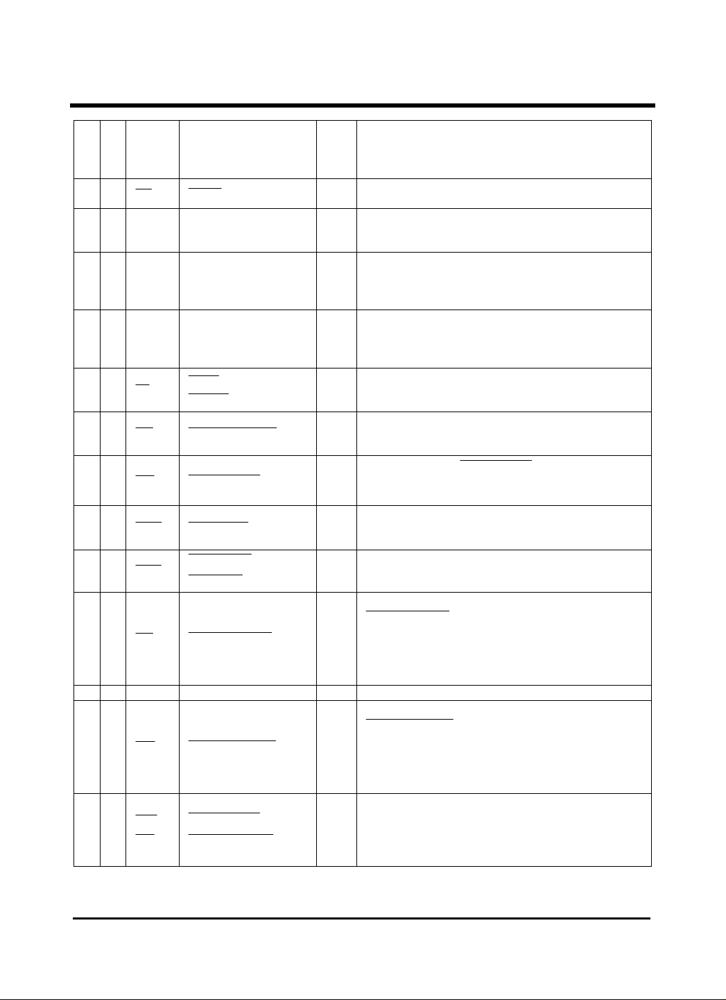
2.3 AC Timing Specifications
GM82C765B
)F32( C0TA °°= to )F158( C70 °° :
SYMBOL
t
CY
Clock Period 60
t
PH
Clock Active (High or Low) 25
t
R
Clock Rise Time (Vin 0.8 to 2.0)
t
F
Clock Fall Time (Vin 2.0 to 0.8)
t
AR
A0, CS,
t
RA
A0, CS,
t
RR
RD Width 90
t
RD
Data Access Time from RD Low
t
DF
DB To Float Delay from RD High 10
t
A0, CS,
AW
t
WA
A0, CS , DACK , LDCR , LDOR , Hold Time from WR High 0
t
WW
t
Data Set Up Time to WR High 80
DW
t
Data Hold Time from WR High 0
WD
t
RI
IRQ Reset Delay Time from RD High 0
t
WI
IRQ Reset Delay Time from WR High 0
t
MCY
DMA Cycle Time 52
t
AM
DMA Reset Delay Time from
t
MA
t
AA
DACK Width 90
t
TC
TC Width 60
t
Reset Width-TTL Driven CLK1 250
RST
t
Reset Width-Software Reset 5
SRST
t
RDD
RDD Active Time Low 40
t
WDD
WD Write Data Width Low 1/2 (TYP) MCY
t
DST
t
STU
t
STP
t
SC
(continued on next page)
Width 60
WR
Delay Time from DMA High 0
DACK
Hold & Set Up to
DIRC
Hold Time from
DSX
Active Time Low 24
STEP
Cycle Time 132
STEP
Set Up Time to RD Low 0
DACK
Hold Time from RD High 0
DACK
DACK,LDCR,LDOR
: pF 100CL
PARAMETER MIN MAX UNITS
nS
nS
nS
nS
nS
nS
nS
nS
nS
, Set Up Time to WR Low 0
nS
nS
nS
nS
nS
1MCY + 150nS
1MCY + 150nS
MCY
DACK
Low
140
nS
nS
nS
nS
nS
MCY
nS
Low 4
STEP
Low 20
STEP
MCY
MCY
MCY
MCY
Page 8

8
48
uS
SYMBOL
t
IDX
IDX Index Pulse Width 2
t
STD
t
MR
RD Delay from DMA 0
t
MW
t
MRW
t
Chip Access Delay from RST Low-TTL 32
CA
t
CAS
t
XCA
t
XTS
t
TCR
t
TCW
Note: CY specifies CLK1 or XT1 period
MCY specifies MCLK period, dependent on selected data rate
WCY specifies WCLK period, dependent on selected data rate
DIRC
WR
RD or WR Response from DMA High
Chip Access Delay from
Chip Access Delay from RST-OSC XT1 at 16MHz 500
XT2 Access Delay after RST 9.6MHz 1000
TC Delay from Last DMA or IRQ, RD 0
TC Delay from Last DMA or IRQ, WR 0
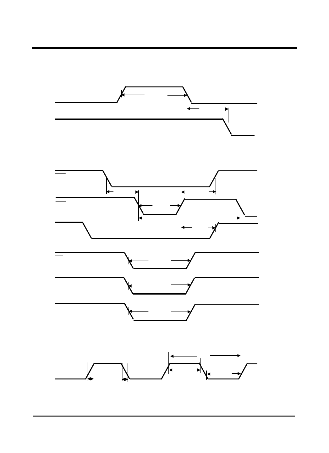
2.4 AC Timing Diagrams
(1) READ Timing
A0
PARAMETER MIN MAX UNITS
Hold Time after
96
STEP
Delay from DMA 0
t
Low 40
SRST
,
.DACK,CS
t
t
t
Data Valid
t
t
t
GM82C765B
MCY
MCY
nS
nS
MCY
MCY
MCY
uS
192 MCY
384 MCY
Page 9

9
WR
DATA
IRQ
Data Valid
tAW
tWW
tWA
tWD
tWI
tDW
DMA or IRQ
TC
tCR
tCW
tTC
tMCY
tMA
tAM
tAA
tMRW
tMR
tRD
tDW
tDF
tWD
Data Valid
DMA
DACK
DATA
RD
orWR
(2) WRITE Timing
(3) TERMINAL COUNT (TC) COUNTING
(4) DMA TIMING
,A0
DACK,CS
tMW
GM82C765B
Page 10
10
CS
DIRC
STEP DSX
WD
(5) RESET Timing
(6) DISK DRIVE SELECT TIMING
(7) CLOCK Timing
RESET
CLOCK
tR
tDST
tF
tRST
tSTP
tIDX
tRDD
tWDD
tPH
GM82C765B
tCA
tSTD
tSC
tSTU
tCY
tPH
Page 11

11
REGISTER
STATUS REG
SEPARATOR
24 × 8
DECODE
PRECOMPENSATION
BUS
TC
DMA
IRQ
A0
CLK1
CLK2
SCLK
MCLK
WD
PCVAL
01
02
WCLK
WRCSDACK
LDCR
LDORHSSTEP
DIRC
RWC
4
1DS
−
TROOWP*
DCHG
WE
3. ARCHITECTURE
The GM82C765B Floppy Disk Subsystem
Controller is a CMOS LSI device that provides
all the needed functionality between the host
u-processor peripheral Bus and the cable
Connec-tor to the Floppy Disk Drive. This CHIP
in-tegrates; Formatter/Controller Data Separation,
Write Precompensation, Data rate Seletion,
Clock generation, Drive interface drivers and
receivers.
8 Bit
DATA
CONTROL
MASTER
HOST
INTERFACE
CLOCK
AND
TIMING
GENERATOR
ALU
MS
SATE
MACHINE
CRYSTAL
OSc×2
DIGITAL DATA
DATA ENCODER
DECODER
Fig 1. GM82C765B Internal Block Diagram
GM82C765B
HOST INTERFACE
The host interface is the host microprocessor
peripheral bus. This bus is composed of eight
control signals and eight data signals. In the
special or PC AT modes, IRQ and DMA request
are tri-stated and qualified enable, internally
provided by the operations register. The data bus,
DMA, and IRQ outputs are designed to handle 20
LS-TTL loading.
DATA
8 Bit INTERNAL DATA BUS
RAM
INSTRUCTION
PROGRAM
FLAG
CRC GENERATOR
ROM
1KÏ16
OPERATION
WRITE
DISK
INTERFACE
CONTROL
REGISTER
Page 12

12
GM82C765B
40 VCC
2.WR
4 A0
3 17 18
22 DRV
*
40
36
37
27
26
29
28
25 1 30
2DS 32
VCC
* PLCC version of
Fig 2. TYPICAL GM 82C765B APPLICATION SYSTEM
Inputs, except the data bus, are Schmitt
trig-ger receivers and can be hooked up to a bus
or backplane without any additional buffering.
During the command or result phases, the
main status Register must be ready by the
processor before each byte of information is
written into or read from the data Register. After
each byte of data is read from or written into the
data Register, the CPU should wait for 12uS
before reading the main status Register. Bits D6
and D7 in the main status Register must be in a 0
and 1 state, respectively, before each byte of the
command word may be written into the
GM82C765B. Many of the command require
multiple bytes. As a result, the Main status
Register must be read prior to each byte transfer
to the GM82C765B. During the result phase,
MICROPROCESSOR
INTERFACE
ADDRESS
RECODE
MAIN
BUS
CKT
CLOCK
CKTS
GND
GND
1 RD
16 IRQ
19 RST
7-14 DB0-DB7
15 DMA
6 TC
24 PCVAL
23 CLK1
21 CLK2
GM82C765B
HDL 35
1MO 3DS 33
34
2MO 4DS
36
RPM RWC
RDD 20
IDX 39
VSS 31
Bits D6 and D7 in the Main status Register must
both be 1’s (D6-1 and D7-1) before reading
each byte from the Data Register. Note that this
regarding of the main status Register before
each byte transfer to the GM82C765B is
re-quired only in the Command and result phases,
and not during the Execution phase. Note also
that DB6 and DB7 in the MSR can be polled
in-stead of waiting 12uS. When they have the
right bit settings, the GM82C765B is ready for
com-mands. This might save some time.
During the Execution phase, the main status
register need not be read. If the GM82C765B
is in the non-DMA Mode, then the receipt of
each data byte is indicated by an interrupt signal
on pin 16 (IRQ-1). The generation of a Read
signal (RD-0) will clear the interrupt as well as
FLOPPY
DISK
DRIVE
INTERFACE
CONNECTOR
GM82C765B
Page 13

13
output the data onto the data bus.
If the processor can not handle interrupt fast
enough (every 13uS for the MFM mode and
27uS for the FM mode), then it may poll the
main status Register and bit D7 (RQM) functions
as the Interrupt signal.
If a Write Command is in process then the
Signal performs the reset to the Interrupt
WR
signal.
All timings mentioned above double for mini
floppy data rates. Note that in the non-DMA
mode it is necessary to examine the main Status
Register to determine the cause of the interrupt
signs is could be a data interrupt or a command
terminaton interrupt, either normal or abnormal.
If the GM82C765B is in the DMA mode, no
inter-rupt signals are generated during the
Execution phase. This signifies the beginning of
the Result phase. When the first byte of data is
read during the Result phase, the Interrupt is
auto-matically cleared (IRQ=0). It should be
noted that in PC AT usage, non-DMA Host
transfers and not the normal procedure. If the
user chooses to do so, the GM82C765B will
successfully complete commands, but will
always give abnormal termination error status
since TC is qualified by an inactive
The RD or WR signals should be asserted
while Dack is true. The CS signal is used in
conjunction with RD and WR as a gating
function during programmed I/O operations.
If the non-DAM mode is chosen, the
signal should be pulled up to
V . It is important
CC
to note that during the Result phase all bytes
shown in the Command Table must be read. The
Read Data Command for example, has several
bytes of data in the Result phase. All seven bytes
must be read Data command. The GM82C765B
will not accept a new command until all seven
bytes have been read. Other commands may
require fewer bytes to be read during the Result
phase. The GM82C765B contains five Status
Registers. The Main Status Registers (ST0, ST1,
ST2, and ST3) are available only during the
Result phase and may be read only after
completing a command.
The particular command that has been
executed determines how many of the Status
Registers will be read.
The byte of data which are sent to the
DACK
.
DACK
GM82C765B
GM82765B to form the command phase, and are
read out of the GM82C765B in the result phase,
must occur in the order shown in the command
Table. The command code must be sent first and
the other bytes sent in the prescribed sequence.
No foreshortening of the command or Result
phase is allowed. After the last byte of data in the
Command phase is sent to the GM83C765B, the
Execution phase of automatically starts. In a
similar fashion, when the last byte of data is read
out in the result phase, the command is
automatically ended and the GM82C765B is
ready for a new command.
CONTROL REGISTER
The Control Register provides support logic that
latches the two LSBs of the data bus upon
receiving
active when this happens. These bits are used to
select the desired data rate, which in turn controls
the internal clock generation. Clock switchover is
internally “deglitched” allowing continuous
operation after change data rates.
If the Control Register is not used, the data rate is
governed by the supplied clock or crystal. The
frequency must be 64X the desired MFM data
rate, up to a maximum frequency of 16 MHz.
This implies a maximum data rate of 250 kb/S.
unless the Control Register is used. Switching
this clock must be “glitchless” or the device will
need to be reset.
Table 1 presents the Control Register.
and WR. CS should not be
LDCR
Page 14

14
GM82C765B
TABLE 1. CONTROL REGISTER
CR1 CR0 DRV DATA RATE COMMENTS RPM (In PC AT MODE)
0 0 X 500K MFM 1
0 0 X 250K FM 1
0 1 0 250K MFM 0
0 1 1 300K MFM 0
1 0 X 250K MFM, RST Default 1
1 0 X 125K FM, RST Default 1
1 1 X 125K 0
MASTER STATUS REGISTER
The Master Status Register is an eight-bit
register that contains the status information of
the FDC, any may be accessed at any time.
Only the Master Status Register may be read
and used to facilitate the transfer of data
between the processor and GM82C765B. The
DIO and RQM bits in the Master Status
Register indicate when data is ready and in
which direction data will be transferred on the
data bus. The maximum time between the last
RD or
during a Command or Result
WR
phase and DIO and RQM getting set is 12us if
500 kb/S MFM data rate is selected. (If 250
kb/s MFM is selected, the delay is 24uS.) For
this reason, everytime the Master Status
Register is read, the CPU should 12us. The
maximum time from the trailing edge of the
last RD in the result phase to when DB4
(FDC busy) goes low is 12 uS.
TABLE 2. MASTER STATUS REGISTER BITs
BIT
NO. NAME SYMBOL
DB0 FDD 0 BUSY D0B FDD number 0 is in the Seek Mode. If any of the bits is set,
FDC will not accept READ or WRITE commands.
DB1 FDD 1 BUSY D1B FDD number 1 is in the Seek Mode. If any of the bits is set,
FDC will not accept READ or WRITE commands.
DB2 FDD 2 BUSY D2B FDD number 2 is in the Seek Mode. If any of the bits is set,
FDC will not accept READ or WRITE commands.
DB3 FDD 3 BUSY D3B FDD number 3 is in the Seek Mode. If any of the bits is set,
FDC will not accept READ or WRITE commands.
DB4 FDC BUSY CB A READ or READ command is in progress. FDC will not accept
any other commands.
DB5 EXECUTION
MODE
DB6 DATA INPUT DI0 Indicates direction of data transfer between FDC and DATA
DB7 REQUEST FOR
MASTER
EXM This bit is set only during Execution phase in non-DMA Mode.
When DBS goes low Execution phase has ended and Results phase
has started. It operates only during non-DMA Mode of operation.
Register. If DIO=1, then transfer is from DATA Register to the
Processor. If DIO=0, transfer is from Processor to the Data Register.
RQM Indicates Data Register is ready to send or receive data to or from
the Process. Both bits DIO and RQM should be used to perform the
handshaking function of “ready” and “direction” to the Processor.
DESCRIPTION
Page 15

15
TABLE 3. STATUS REGISTER 0 BITs
GM82C765B
BIT
NO
D7 INTERRUPT
D6
D5
#D4 EQUIPMENT
#D3 NOT READY NR Since drive ready is always persumed true. This will always be a LOGIC
D2 HEAD SELECT
D1 UNIT SELECT 1 US1 This flag is used to indicate a DRIVE UNIT Number at interrupt
D0 UNIT SELECT 0 US0 This flag is used to indicate a DRIVE UNIT Number at interrupt
NAME SYMBOL
IC D7 = 0 and D6 = 0, Normal termination of command was completed
CODE
D7 = 1 and D6 = 0.
SEEK END SE When FDC completes the SEEK comand, this flag is set to 1 (HIGH)
EC If the Track 0, signal fails to occur after 255 step pulses (Recalibrate
CHECK
HS This flag is used to indicate the state of HEAD at interrupt
properly executed.
D7 = 0 and D6 = 1, Abnormal termination of command (AT).
Execution of command was started but was not successfully completed.
Invalid comand issue, (IC). Command which was issued was never
started.
command). Then this flag is set.
0.
DESCRIPTION
TABLE 4. STATUS REGISTER 1 BITs
BIT
NO
D7 END OF
D6 Not used. This bit is always 0 (low)
D5 DATA ERROR DE When the FDC detects a * CRC error in either the ID field or a cylinder,
D4 OVERRUN OR If the FDC is not serviced by the host system during data transfers within
D3 NOT DATA Not used. This bit is always 0 (low)
D2 NO DATA ND During execution of READ DATA, WRITE DELETED DATA, or SCAN
D1 NOT
NAME SYMBOL
CYCLINDER
WRITEABLE
EN When the FDC tries to access a sector beyond the final sector of a
cylinder,this flag is set.
this flag is set.
a certain time interval, this flag is set.
command, if the FDC cannot find the sector specified in the * * IDR
Register, this flag is set. During execution of the READ ID command, if
the FDC cannot read the ID field without an error, then this flag is set.
During execution of the READ A TRACK command, if the starting sector
cannot be found, then this flag is set.
NW During execution of WRITE DATA, WRITE DELETED DATA or
RORMAT A TRACK commands. If the FDC detects a WP signal from
the FDC, then this flag is set.
DESCRIPTION
Page 16

16
TABLE 4. STATUS REGISTER 1 BITs
BIT
NO
D0 MISSING
NAME SYMBOL
ADDRESS
MARK
MA If the FDC cannot detect the ID Address Mark after encountering the
index hole twice, then this flag is set.
If the FDC cannot detect the Data Address Mark or Deleted Data Address
Mark, this flag is set. At the same time the MD (Missing Address Mark in
data field) of Status Register 2 is set.
TABLE 5. STATUS REGISTER 2 BITs
GM82C765B
DESCRIPTION
BIT
NO
D7 Not Used. This bit is always 0 (low)
D6 CONTROL
D5 DATA ERROR DD If the FDC detects a CRC error in the data field, then this flag is set.
D4 WRONG
D3 SCAN EQUAL SH During execution of the SCAN command, if the condition of “equal” is
D2 SCAN NOT SN During execution of the SCAN command, if the FDC cannot find a sector
D1 BAD
D0 MISSING
NAME SYMBOL
MARK
CYLINDER
CYLINDER
ADDRES
MARK
IN DATA FIELD
CM During executing of the READ DATA or SCAN Command, if the FDC
encounters a sector which contains a Deleted Data Address Mark, this flag
is set.
WC This bit is related to the ND bit, and when the contents of * * * C on the
medium is different from that stored in the IDR, this flag is set.
satisfied this flag is set.
on the cylinder which meets the condition, then this flag is set.
BC This bit is related to the ND bit, and when the contents of C on the
medium is different from that stored in the IDR, and the contents of C is
FF, then this flag is set.
MD When data is read from the medium, if the FDC cannot find a Data
Address Mark or Deleted data Address Mark, then this flag is set.
DESCRIPTION
TABLE 6. STATUS REGISTER 3 BITs
BIT
NO
#D7 Not used. Will always be logic 0.
D6
#D5 READY RY
D4 TRACK 0 TO This bit is used to indicate the status of the Track 0 signal from the FDD.
#D3
D2 HEAD SELECT
D1 UNIT SELECT 1
D0 UNIT SELECT 2
NAME SYMBOL
WRITE
PROTECTED
WRITE
PROTECTED
CYLINDER
WP
WP
HS This bit is used to indicate the status of the Side Select signal to the FDD
US1
US0
signal from the FDD
This bit will always be a logic 1.
Drive is presumed to be ready.
This bit is used to indicate the status of the WRITE PROTECTED
signal from the FDD
This bit is used to indicate the status of the Unit Select 1 signal to the
FDD
This bit is used to indicate the status of the Unit Select 0 signal to the
FDD
This bit is used to indicate the status of the
Note : * CRC - Cyclic Redundancy Check
* * IDR - internal Data Register
* * * C - Cylinder
# - Different from NEC765
DESCRIPTION
WRITE PROTECTED
Page 17

17
RD
RD
* DATA REGISTER
GM82C765B
The eight-bit data Register stores data, commands, parameters, and FDD status information.
Data bytes are read out of, or written into, the
Data Register in order to program or obtain the
results after a particular command.
The relationship between the Master Status
Register and the Data Register Status Register
and the Data Register and the signals
,WR, and A0 are shown in Table 7.
TABLE 7. MASTER STATUS AND DATA REGISTERS Relationships
A0
0
0
0
1
1
1
WR FUNCTION
0
1
0
0
0
1
1
0
0
0
1
0
Read Main Status Register
ILLEGAL
ILLEGAL
ILLEGAL
READ from DATA REGISTER
WRITE into DATA REGISTER
* OPERATIONS REGISTER
The Operations Register provides support logic
that latches the data bus upon receiving
ad WR. CS should not be active
LDOR
when this happens. The Operations
Register replaces the typical latched port found
.
in floppy subsystems used to control disk drive
spindle motors and to select the desired disk
drive. Table 8 represents the operations
Register
TABLE 8. OPERATIONS REGISTER
OR0
OR1
OR2
OR3
OR4
OR5
OR6
OR7
DSEL
(X)
SRST
DMAEN
MOEN1
MOEN2
(X)
(MSEL)
: Drive Select, if low and MOEN1 = 1, then
MOEN2 = 1, then
: In GM82C765B this mist be logic 0 for 1DS and
No defined function in GM82C765B.
: Soft reset, active low.
: DMA enable, active in Special and PC AT modes, Qualifies DMA and IRQ
outputs and
: Motor On enable, inverted output
: Motor On enable, inverted output 2MO is active in PC AT
: Has no defined function. A spare.
: Mode Select, During a soft reset condition, may be used to select
between Special mode (1) and PC AT mode (0).
DACK
is active. If high and
1DS
is active, but only in the PC AT mode
2DS
to become active.
2DS
input.
is active only in PC AT
1MO
Page 18

18
RPM
* BASE, SPECIAL, AND PC AT MODES
Base, Special, and PC AT modes allow subtle
differences which the user may find desirable.
The Control Register may be used in any mode
without altering functionality.
* BASE MODE
After a hardware reset, RST active, the
GM82C765B will be held on soft reset,
active, with the normally driven signals, DMA
request and IRQ request outputs tristated. Base
mode may be initiated at this time by a chip
access by the host. Although this may be any
read or write, it is strongly recommended that
the Base mode user’s first chip access be a read
of the Master Status Register. Once Base mode
is entered, the soft reset is released, and IRQ
and DMA are driven. Base mode prohibits the
use of the Operations Register, hence there can
be no qualifying by DMAEN and no soft resets.
The Drive Select outputs,
1DS
to
a 1 of 4 decoding of the Unit Select bits
resident in the command structure.
Pin
represents Reduce Write Current
RWC
and is indicative of when write
precompensation is necessary.
SRST
, offer
4DS
GM82C765B
AT mode can also be entered from Special
mode by loading the Operations Mode Select
to a logic 0, disabling MOEN1 and MOEN2,
and causing
of the Control Register address sets the device
into PC AT mode. The DS outputs are now
replaced with the DSEL and MOEN signals
buffered from the Operations Register.
DMAEN and
compatible with the current BIOS.
pinfunction is now
two speed drives may reduce spindle speed per
minute to 300 revolutions per minute when
active low, used to reduce write current when a
slower data rate is selected for a given drive.
Figure 3 illustrates the relationship among the
three modes.
to be active. Then a read
SRST
are supported and
SRST
so that users with
RWC
* SPECIAL MODE
Special mode allows use of the Operations
Register for the DMAEN signal as a qualifier
and to do a software driven device reset,
. To enter Special mode, the Operations
SRST
Register is loaded with (1X00X0XX), setting
mode Select to a logic 1 disabling MOEN1 and
MOEN2 and causing SRST to be active.
Then a read of the Control Register address,
and RD, will set the device into
LDCR
Special mode. The
again offered in this mode, as is
through
1DS
RWC
.
is
4DS
* PC AT Mode
For PC AT compatibility, users will write to
the Operations Register,
this action, performed after a hardware reset,
or in the Base mode, initiates PC AT mode. PC
LDOR
and
WR
;
Page 19

19
READ MASTER
STATUS REG.
BASE
MODE
Fig. 3 Flow Diagram Depicting Relationship of Base, Special, and PC AT
modes.
l POLLING ROUTINE
DS1
DS2
DS3
DS4
HARDWARE
RESET
WRITE TO
OPER REG.
PC AT
MODE
WRITE 80 TO
OPER REG
READ CONT REG
LDCR, RD
SPECIAL
MODE
WRITE 00 TO
OPER REG
READ CONT
REG. LDCR, RD
Fig. 4. Drive select polling timing
GM82C765B
After any reset the GM82C765B, (a hard
RST or soft
a Polling routine. In between commands (and
between step pulse in the SEEK Command),
the GM82C765B polls all four FDDs looking
for a change in the ready line from any of the
drives. Since the drive is always presumed
ready, an interrupt will only be generated
following a reset. This occurs because a reset
forces Not ready status, which then promptly
becomes ready.
Note that in special or PC AT mode if
DMAEN is not valid prior to 1mS after reset
goes inactive, then IRQ may be already set and
pending when finally enabled onto the bus.
The polling of the ready line by the
GM82C765B occurs continuously between
commands. Each drive is polled every
1,024mS, except during the READ/WRITE
commands. For minifloppies, the polling rate is
2,048mS. The drive polling sequence is
1-2-4-3. Please note that in the PC AT mode,
the user will not see the polling at the Drive
Select signals, figure 4 illustrates the Drive
Select Polling time
, will automatically go into
SRST
* DEVECE RESETS
The GM82C765B supports both hardware reset
(RST) pin (19) and a software reset (
SRST
through use of the Operations Register. The RST
pin will cause a device reset for the active
duration. RST causes a default to Base mode, and
default selects 250k MFM (or 125k FM, code
dependent) as the data rate (16 MHz input clock).
will reset the microcontroller as did the
SRST
If the XTAL oscillators are used, instead of the
TTL driven clock inputs, the hardware RST
)
active time requirement will bootstrap the circuit
into guaranteed oscillation in a fixed amount of
time.
The extended reset time allows the growth of the
oscillation to produce stable internal clock timing
RST, but will not affect the value set for the
internal timers-HUT, FTL, and SRT.
Page 20

20
∗
DATA SEPARATOR
The Data Separator is a Digital Phase Lock
Loop Floppy Disk Data Separator (DPLL). It was
designed to address high performance error rates on
floppy disk drives, and to provide superior
performance in terms of available bit jitter tolerance. It
contains the necessary logic to achieve classical 2nd
order, type 2, phase locked loop performance. DPLL is
used as the Data Separator in the GM82C765B system.
Figure 5 illustrates the DPLL implified block diagram.
The bit jitter tolerance for the data separator is 60%,
Which guarantees an error rate of < 10E-9.
∗
WRITE PRECOMPENSATION
The BM82C765B maintains the stand first level
algorithm to determine when write precompensation
should be applied.
The EARLY and LATE signals are used internally to
DSKD
DATA
SYNCHRONIZATION
P
H
A
S
E
DETE-
CTION
TRANSIENT RESPONSE
STATE FILTERING
STEADY STATE
FREQUENCY
FILTERING
REFCLK
CLOCK GENERATION
CD1
CD2
Fig. 5. DPLL Simplified BLOCK DIAGRAM
GM82C765B
select the appropriate delay in the write data pulse
stream.
The encoded WRITE DATA signal is synchronized to
the 16 MHz clock if this is the frequency on CLK1 pin
(23), and clocked through a shift register before a
multiplexer gates the chosen bit to the output.
The output data pulse width has a 25% duty cycle,
i.e., one fourth of the bit cell period, and equal to one
half the WCLK period.
When PCVAL pin (24) = 1, all data will be
precompensated by + 187nS precompensation will be
generated. For frequencies other than 16 MHz on the
CLK1 pin, the precompensation values will be two and
three clock cycles respectively.
When the non-standard data rate using CLK2 is chosen,
the MFM precompensation will always be two clock
cycles.
For 9.6MHz, this is +208nS. In this case, this PCVAL
function is disabled
Phase
SEPCLK
DIGITAL
CONTROLLED
OSCILLATOR
SCLK
RDATA
RESYNCHRONIZATIO
SUMMER
SEPD
SEPCLK
Page 21

21
23 22
XT2
RESONANT
* CLOCK GENERATION
GM82C765B
TABLE 9. CLOCK DATA RATE
This logical block provides all the clocks needed by
the GM82C765B. They are: Sampling clock (SCLK),
Write clock (WCLK), and the MASTER CLOCK
(MCLK). SCLK drives the DPLL Data Separator used
during data recovery. This Clocks’s frequency is
always 32 times the selected data rate. WCLK is used
by the encoder logic to place MFM or FM on the serial
WD-stream to the disk. WCLK always has a frequency
two times the selected data rate. MCLK is used by the
microsequencer. MCLK and MCLK clock all latches
in a two-phase scheme.
One microinstruction cycle is four MCLK cycles.
MCLK has a frequency times the FM data rate.
Table 9 presents the Clock Data Rate. Figure 6
illustrates the XTAL oscillator circuits for the 44-pin
PLCC configuration.
XT1
XT1
26
C
4
25
C
3
XT2
XT2
C
1
C
2
DATA RATE CODE SLCK MCLK WCLK
500Kbit/S MFM 16.0MHz 4.0MHz 1.0MHz
250Kbit/S FM 8.0MHz 4.0MHz 500.0MHz
250Kbit/S MFM 8.0MHz 2.0MHz 500.0MHz
125Kbit/S FM 4.0MHz 2.0MHz 250.0MHz
300Kbit/S MFM 9.6MHz 2.4MHz 600.0MHz
9.6MHz + 100 ppm
R Series = 30 ohm Max
C Shunt = 10 pf Max
C1 = 68 pf 5% mica
C2 = 56 pf 5% mica
9.6MHz + 100 ppm
R Series = 30 ohm Max
C Shunt = 10 pf Max
C3 = 47 pf 5% mica
C4 = 15 pf 5% mica
SERIES RESONANT
SERIES
Fig 6. XTAL Oscillator circuits for the 44 pin PLCC
Page 22

22
∗
COMMAND PARAMETERS
GM82C765B
TABLE 10. GM82C765B COMMANDS
The GM82C765B is capable of performing 15
different commands. Each command is initiated by a
multibyte transfer from the processor. The results
after execution of the command may also be a
multibyte transfer back to the processor. The
commands consist of three phases : Command phase,
Execution phase, and the Result phase.
Command phase − The Floppy Disk Controller
(FDC) receives all information
required to perform a
particular operation from the
processor.
Execution phase − The FDC performs the operation
it was in structed to do.
Result phase − After completion of the operation,
status and other housekeeping in
formation are made available to the
processor
READ DATA
READ DELETED DATA
WRITE DATA
WRITE DELETED DATA
READ A TRACK
READ ID
FORMAT A TRACK
SCAN EQUAL
SCAN LOW OR EQUAL
SCAN HIGH OR EQUAL
Table 10. lists the 15 GM82C765B commands.
Table 11. through 25 are presented to show the
required parameters and results for each command.
Most commands require nine command bytes during
the result phase. The “W” to the left of each byte
indicates a command phase byte to be written. An
“R” indicates a result byte.
TABLE 11. READ DATA
PHASE R/W D7 D6 D5 D4 D3 D2 D2 D0 REMARKS
COMMAND
EXECUTION
RESULTS
W W MT X MF X SK X 0
W
W
W
W
W
W
W
R
R
R
R
R
R
R
X
0 X 1
C
H
R
N
EOT
GPL
DTL
STO
ST1
ST2
C
H
R
N
HS 1 US1 0 US0
Command Codes
Sector ID information prior to
command execution. The four bytes
are compared against header on
floppy disk.
Data transfer between FDD and main
system
Status information after command
execution.
Sector ID information after command
execution.
Page 23

23
TABLE 12. READ DELETED DATA
COMMAND
EXECUTION
RESULTS
TABLE 13. WRITE DATA
PHASE R/W D7 D6 D5 D4 D3 D2 D2 D0 REMARKS
COMMAND
EXECUTION
RESULTS
R/W D7 D6 D5 D4 D3 D2 D2 D0 REMARKS
W W MT X MF X SK X 0
X
W
W
W
W
W
W
W
R
R
R
R
R
R
R
W W MT X MF X 0 X 0
X
W
W
W
W
W
W
W
R
R
R
R
R
R
R
C
H
R
N
EOT
GPL
DTL
STO
ST1
ST2
C
H
R
N
C
H
R
N
EOT
GPL
DTL
STO
ST1
ST2
C
H
R
N
1 X 1
HS 0 US1 0 US0
0 X 1
HS 0 US1 1 US0
Command Codes
Sector ID information prior to
command execution. The four bytes
are compared against header on floppy
disk.
Data transfer between FDD and main
system
Status information after command
execution.
Sector ID information after command
execution.
Command Codes
Sector ID information prior to
command execution. The four bytes
are compared against header on
floppy disk.
Data transfer between FDD and main
system
Status information after command
execution.
Sector ID information after command
execution.
GM82C765B
Page 24

24
TABLE 14. WRITE DELETED DATA
PHASE R/W D7 D6 D5 D4 D3 D2 D2 D0 REMARKS
COMMAND
EXECUTION
RESULTS
TABLE 15. READ A TRACK
PHASE R/W D7 D6 D5 D4 D3 D2 D2 D0 REMARKS
COMMAND
EXECUTION
RESULTS
W W MT X MF X 0 X 0
W
W
W
W
W
W
W
R
R
R
R
R
R
R
W W 0 X MF X SK X 0
W
W
W
W
W
W
W
R
R
R
R
R
R
R
X
X
1 X 0
C
H
R
N
EOT
GPL
DTL
STO
ST1
ST2
C
H
R
N
C
H
R
N
EOT
GPL
DTL
STO
ST1
ST2
C
H
R
N
HS 0 US1 1 US0
0 X 0
HS 1 US1 0 US0
Command Codes
Sector ID information prior to
command execution. The four bytes
are compared against header on
floppy disk.
Data transfer between FDD and main
system
Status information after command
execution.
Sector ID information after command
execution.
Command Codes
Sector ID information prior to
command execution.
Data transfer between FDD and main
system. FDD reads all data fields from
index hole to EOT
Status information after command
execution.
Sector ID information after command
execution.
GM82C765B
Page 25

25
TABLE 16. READ ID
PHASE R/W D7 D6 D5 D4 D3 D2 D2 D0 REMARKS
COMMAND
EXECUTION
RESULTS
TABLE 17. FORMAT A TRACK
PHASE R/W D7 D6 D5 D4 D3 D2 D2 D0 REMARKS
COMMAND
EXECUTION
RESULTS
W W 0 X MF X 0 X 0
R
R
R
R
R
R
R
W W 0 X MF X 0 X 0
W
W
W
W
R
R
R
R
R
R
R
X
X
1 X 0
STO
ST1
ST2
C
H
R
N
N
SC
GPL
D
STO
ST1
ST2
C
H
R
N
HS 1 US1 0 US0
1 X 1
HS 0 US1 1 US0
Command Codes
The first correct ID information on the
cylinder is stored in Data Register.
Status information after command
execution.
Sector ID information after command
execution.
Command Codes
Bytes / Sector
Sector/Track
Gap 3
Filler Byte
Floppy Disk Controller (FDC) formats
an entire track.
Status information after command
execution.
In this case, ID information has no
meaning.
GM82C765B
Page 26

26
TABLE 18. SCAN EQUAL
PHASE R/W D7 D6 D5 D4 D3 D2 D2 D0 REMARKS
COMMAND
W W MT X MF X SK X 1
X
0 X 0
HS 0 US1 1 US0
Command Codes
GM82C765B
EXECUTION
RESULTS
W
W
W
W
W
W
W
R
R
R
R
R
R
R
C
H
R
N
EOT
GPL
STP
STO
ST1
ST2
C
H
R
N
Sector ID information prior to command
execution.
Data transfer between FDD and main
system
Status information after command
execution.
Sector ID information after command
execution.
TABLE 19. SCAN LOW OR EQUAL
PHASE R/W D7 D6 D5 D4 D3 D2 D2 D0 REMARKS
COMMAND
EXECUTION
RESULTS
W W MT X MF X SK X 1
W
W
W
W
W
W
W
R
R
R
R
R
R
R
X
1 X 0
C
H
R
N
EOT
GPL
STP
STO
ST1
ST2
C
H
R
N
HS 0 US1 1 US0
Command Codes
Sector ID information prior to ommand
execution.
Data transfer between FDD and main
system
Status information after command
execution.
Sector ID information after command
execution.
Page 27

27
TABLE 20. SCAN HIGH OR EQUAL
PHASE R/W D7 D6 D5 D4 D3 D2 D2 D0 REMARKS
COMMAND
W W MT X MF X SK X 1
X
1 X 1
HS 0 US1 1 US0
Command Codes
GM82C765B
EXECUTION
RESULTS
W
W
W
W
W
W
W
R
R
R
R
R
R
R
C
H
R
N
EOT
GPL
STP
STO
ST1
ST2
C
H
R
N
Sector ID information prior to command
execution.
Data transfer between FDD and main
system
Status information after command
execution.
Sector ID information after command
execution.
TABLE 21. RECALIBARTE ∗
PHASE R/W D7 D6 D5 D4 D3 D2 D2 D0 REMARKS
COMMAND
EXECUTION Head retracted to Track zero
W W 0 X 0 X 0 X 0
X
0 X 1
HS 1 US1 1 US0
Command Codes
TABLE 22. SENSE INTRRUPT STATUS
PHASE R/W D7 D6 D5 D4 D3 D2 D2 D0 REMARKS
COMMAND W 0 0 0 0 0 1 1 1 Command Codes
RESULTS R
Status information about the FDC at
the end of seak operation
TABLE 23. SPECIFY
PHASE R/W D7 D6 D5 D4 D3 D2 D2 D0 REMARKS
W
EXECUTION
0 0 0 0 0 0 1 1 COMMAND
W
SRT HUT
HLT
Command Codes
N D
Head retracted to Track zero
Page 28

28
GM82C765B
TABLE 24. SENSE DRIVE STATUS
PHASE R/W D7 D6 D5 D4 D3 D2 D2 D0 REMARKS
COMMAND
EXECUTION ST3 Status information about the FDC
W W 0 X 0 X 0 X 0
X
0 X 0
HS 0 US1 0 US0
Command Codes
TABLE 25. SEEK
COMMAND
EXECUTION
Table 26 defines, in alphabetical order, the symbols used in Command Tables 11 through 25.
R/W D7 D6 D5 D4 D3 D2 D2 D0 REMARKS
W
W
W
0 X 0 X 0 X 0
X
NCN
1 X 1
HS 1 US1 1 US0
Command Codes
Head is positioned over proper cylinder
on the diskette.
TABLE 26. COMMAND SYMBOL DESCRIPTIONS
SYMBOL NAME DESCRIPTION
A0 ADDRESS LINE 0
C CYLINDER NUMBER C stands for the current/selected cylinder (track) numbers 0 through 255 of the
D DATA
D7-D0 DATA BUS
DTL DATA LENGTH
EOF END OF TRACK
GPL GAP LENGTH
H HEAD ADDRESS H stands for head number 0 or 1, as specified in the ID field.
HLT HEAD LOAD TIME HLT stands for the HEAD LOAD TIME in FDD (2 to 254ms in 2ms increments)
HS HEAD SELECT
HUT HEAD UNLOAD TIME
MF FM or MFM
A0 Controls selection of Main Status Register (A0 = 0) or Data Register (A0 =1)
medium.
D stands for the data pattern which is going to be written into a sector.
8-bit DATA BUS, where D7 stands for a most significant bit, and D) stands for a
least significant bit.
When N is defined as 00, DTL stands for the DATA LENGTH which users are
going to read out or write into the sector.
EOT stands for the final sector number on a cylinder. During read or Write
operations. FDC will stop data transfer after a sector number equal to EOT.
GPL stands for the length of Gap 3. During the FORMAT Command. It
determines the size of Gap 3.
HS stands for a selected head number 0 or 1 and controls the polarity of pin 25
(in 40 pin DIP) or pin 28 (in 44 pin PLCC)
HUT stands for the HEAD UNLOAD TIME after a Read or Write operation has
occurred (16 to 240ms in 16ms increments).
If MF is low, FM mode is selected. If it is high, MFM mode is selected.
MT
MULTITRACK
If MT is high, a MULTITRACK operation is performed.
If MT =1 after finishing Read / Write operation on side 0, FDC will
automatically start searching for sector 1 on side 1
Page 29

29
SYMBOL NAME DESCRIPTION
N NUMBER N stands for the NUMBER of data bytes written in a sector.
NCN
ND NON-DMA MODE ND stands for operation in the NON-DMA MODE.
PCN PRESENT CYLINDER
R RECORD R stands for the sector number which will be read or written.
R/W READ/WRITE R/W stands for either READ or WRITE signal.
SC SECTOR SC indicates the number of sectors per cylinder.
SK SKIP SK stands for SKIP Deleted Data Address mark.
SRT STEP RATE TIME
ST0
ST1
ST2
ST3 STATUS 3
STP
US0, US1 UNIT SELECT US stands for a selected drive; binary encoded, 1 of 4.
NEWCYLINDER
NUMBER
STATUS 0
STATUS 1
STATUS 2
NCN stands for a NEW CYLINDER NUMBER which is going to be reached as
a result of the Seek operation. Desired position of head.
PCN stands for the cylinder number at the completion of the SENSE
INTERRUPT STATUS Command position of head at present time..
STR stands for the Stepping Rate for the FDD (1 to 16ms in 1ms increments).
Stepping Rate applies to all drives. In 2’s complement format, F(Hes) = 1ms,
E(Hex) =2ms, etc
STO = 3 stands for one of four registers which store the STATUS information
after a command has been executed. This information is available during the
result phase after command execution.
These registers should not be confused with the main Status Register (selected by
A0 = 0). ST0=3 may be read only after 3 command has been executed and
contains information relevant to that particular command.
During a SCAN operation, if STP=1, the data in contiguous sectors is compared
byte by byte with data sent from the processor (or DMA); if STP=2, then
alternate sectors are read and compared.
GM82C765B
COMMAND DESCRIPTIONS
Read Data
A set of nine byte words are required to place the
FDC into the Read Data Mode.
After the Read Data command has been issued,
the FDC loads the head (if it is unloaded state),
warts the specified head setting time (defined in
the Specify Command begins reading ID Address
Marks and ID fields. When the current sector
number (“R”) stored in the ID Register (IDR)
compares with the sector number read off the
diskette, then the FDC outputs data (from the
data bit) byte-to-byte to the main system via the
data bus.
After completion of the read operation from the
current sector, the Sector number is incremented
by one, and the data from the next sector is read
and output on the data bus.
This continuous read function is called a
“Multi-sector Read Operation.” The Read Data
Command may be terminated by the receipt of a
Terminal Count signal.
TC should be issued at the same time that the
for the last byte of data is sent.
DACK
Upon receipt of this signal, the FDC stops
outputting data to the processor, but will continue
to read data from the current sectors, check CRC
(Cyclic Redundancy Count) bytes, and the end of
the sector terminate the read data command.
The amount of data which can be handled with a
single command to the FEC depends upon MT
(multi-track), MF(MFM/FM), and N(number of
bytes/sector). Table 27 lists the transfer Capacity.
The “Multi-track” function (MT) allows the FDC
to read data from both sides of the diskette. For a
particular cylinder, data will be transferred
starting at Sector 1, Side 0 and
completing at Sector L, Side 1 (Sector L = last
sector on the side). Note, this function pertains to
only one cylinder (the same track) on each side of
the diskette.
When N=0, then DTL defines the data length
which the FDC must treat as a sector. If DTL is
smaller than the actual data length in a sector, the
Page 30

30
GM82C765B
data beyond DTL in the sector is not sent to the
Data Bus. The FDC reads (internally) the
complete sector performing the CRC check, and
depending upon the manner of command
termination, may perform a Multi-Sector Read
operation. When N is non-zero, then DTL has no
meaning and should be set to FF Hexadecimal.
TABLE 27. TRANSFER CAPACITY
Multi-
track
MT
0 0 0 1 00
1 1 0 1 00
0 0 0 1 01
1 1 0 1 01
0 0 0 1 02
1 1 0 1 02
MFM/FM
MF
Bytes/
Maximum Transfer
Sector
N
(Number of Sectors)
(128) (26) – 3.328
01
(256) (26) – 6.656
(128) (52) – 6.658
01
(256) (52) –13.312
(256) (15) – 3.840
02
(512) (15) – 7.680
(256) (30) – 7.680
02
(512) (30) – 15,360
(512) (8) – 4.096
03
(1024) (8) – 8.192
(512) (16) – 8.192
03
(1024) (16) – 16.384
Capacity
26 at Side 0
or 26 at Side 1
15 at Side 0
or 15 at Side 1
15 at Side 1
or 8 at Side 1
At the completion of the Real data Command,
the head is not unloaded until after head unload
time interval (specified in the specify Command)
has elapsed. If the processor issues another
command before the head unloads, then the head
setting time may be saved between subsequent
reads. This time out is particularly valuable when
a diskette is copied from one drive to another.
If the FDC detects the index Hole twice
without finding the right sector, (indicated in ‘R’ ),
then the FDC sets the ND (No Data) flag in status
Register 1to a 1 (high), and terminates the Read
Data command (Status Register 0 also has bits 7
and 6 set to 0 and 1 respectively.)
After reading the ID and Data Fields in each
sector, the FDC checks the CRC bytes If a read
error is detected (incorrect CRC in ID field), the
FDC sets the DE(Data Error) flag in Status
Register 1 to 1 (High) If a CRC error occurs in
the data field, the FDC also sets the DD(Data
Error in Data Field) flag in Status Register 2 to
1(High) and terminates the Read data command.
(Status Register 0 also has bits 7 and 6 set to 0
and 1 respectively.)
If the FDC reads a Deleted Data Address Mark
Final Sector
Read from
Diskettes
26 at Side1
8 at Side 0
8 at Side 1
off the diskette, and the SK bit (bit D5 in the first
Command Word) is not set (SK =0), then the
FDC sets the CM(control Mark) flag in Status
Register 2 to a 1 (high), and terminates the Read
Data command, after reading all the data in the
sector. If SK = 1, the FDC skips the sector with
the Deleted Data Address Mark and reads the
next sector. The CRC bits in the deleted data field
are not checked when SK = 1.
During disk Data transfers between the FDC and
the processor, via the data bus, the FDC must be
serviced by the processor every 27 us in the FM
mode, land every 13 us in the MFM mode, or the
FDC sets the OR (Overrun) flag in status Register.
1 to a 1 (high), and terminates the Read Data
command.
TABLE 28. C, H, R, and VALUES
MT HD
0
1
Notes : NC (No Change) : The same value the one at the beginning
Final Sector
Transferred
to processor
0 Less then EOT NC NC R+1 NC
0 Equal to EOT C+ 1 NC R=01 NC
1 Less then EOT NC NC R+1 NC
1 Equal to EOT C+1 NC R=01 NC
0 Less then EOT NC NC R+1 NC
0 Equal to EOT NC LSB R=01 NC
1 Less then EOT NC NC R+1 NC
1 Equal to EOT C+1 LSB R=01 NC
of command execution. LSB (Least Significant Bit): The
Least significant bit of H is complemented.
ID information at Resul t Phase
C H R N
Page 31

31
Write Data
A set of nine bytes is required to set the into
DC the Write Data mode, after the commawrite
data and has been issued the FDC loads the head
(if is in the unloaded state), waits the specified
head settling time (defined in the specify
command), and beings reading ID fields, when
all four bytes loaded during the command
(C,H,R,N) match the four byte of ID field from
the processor byte-by-byte via the data bus and
outputs it to the FDD. After writing data into the
current sector, the sector number stored in ‘Rr’ is
incremented by one, and the next data field is
written into. The FDC continues this multisector
Write Operation’ until the issuance of Terminal
Count signal. If a Terminal Count signal is sent
to the FDC it continues writing into the current
sector to complete the data field. If the Terminal
Count signal is received while a data field is
being written remainder of the data field is filled
zeros.
The FDC reads the ID field of each sector
and checks the CRC bytes. If the FDC detects a
read error (CRC error) in one of the ID fields, it
sets the DE (DATA Error) flag of Status Register
1 to a 1 (high) and terminates the Write Data
command. (Status Register 0 also has bit 7 and 6
set to 0 and 1 respectively.)
The Write command operates in much the
same manner as the Read command. The
following items are the same., and one should
refer to the Read data command for details.
The Write command operates in much the
same manner as the Read command. The
following items are the same, and one should
refer to following items are the same, and one the
Read Data command for details:
• Transfer capacity
• EN (End of Cylinder) flag
• ND (No Data) flag
• Head Unload Time interval
• ID information When the processor
terminates command
•Definition of DTL when N=0 and when N=0
In the Write Data mode, data transfers
between the processor and FDC via the data bus,
GM82C765B
must occur every 27 uS in the FM mode and
every 13 us in the MFM mode. If the time
interval between data transfers is longer than this,
then the FDC sets the OR (Overrun) flag in
Status Register 1 to a 1 (high) and terminal the
Write Data Address mark.
Write Deleted Data
This command is the same as the Write Data
command except a Deleted Data Address mark is
written at the beginning of the data field instead
of the normal Data Address mark.
Read Deleted Data
This command is the same as the Read Data
command except that when the FDC detects a
Data Address mark at the beginning of a data
field (and SK = 0 (low)), it will read all the data
in the sector and set the CM flag in Status
Register 2 to a 1 (high), and then terminate the
command. If SK = 1, then the FDC skps the
sector with the Data Address mark and reads the
next sector.
Read A Track
This command is similar to the Read Data
command except that this is a continuous Read
operation where the entire data field from each of
the sectors is read. Immediately of the sectors is
read. Immediately after sensing the index hole.
The FDC starts reading all data fields on the
track as continuous biocks of data.
If the FDC finds an error in the ID or Data
CRC check bytes, it continues to. This command
terminates when the number of sectors read is
equal to EOT. If the FDC does not find an ID
Address mark on the diskette after it senses index
hole for the second time, it sets the MA (Missing
Address mark) flag in Status Register 1 to a 1
(high) and terminates the command. (Status
Register 0 has bits 7 and 6 set to 0 and 1
respectively.)
Page 32

32
00
01
02
03
04
05
01
02
30
05
06
00
00
01
02
03
04
01
01
02
03
04
05
0
1
2
1
2
3
GM82C765B
READ ID
The Read ID command is used to give the
present position of the recording head. The FDC
stores the values from the first ID field it is able
to read. If no proper ID Address mark is found on
the diskette before the index hole is encountered
for the second time, then the MA (Missing
Address mark) flag in Status Register 1 is set to a
1 (high), and if no data is found then the ND (No
Data) flag is also set in Status Register 1to a 1 to
a 1 (high). The command is then terminated with
bits 7 and 6 in Status Register 0 set to 0 and 1
respectively. During this command there is no
data transfer between FDC and the CPU except
during the result phase.
Format A Track
The format command allows an entire track to
be formatted. After the index hold is detected,
data is written on the diskette; Gaps , Address
marks, ID fields and data fields, all per the IBM
System 34 (double density) or System 3740
(single density ) format are recorded. The
particular format which will be written is
controlled by the values Programed into N
(number of bytes/sector), SC (secros/cylinder),
GPL (gap length), and D (data pattern) which are
supplied by the processor during the Command
phase. The data field for each sector is supplied
by the processor; that is four data requests per
sector are made by the FDC for C (cylinder
number). H (Head number), R (sector number)
and N (number of bytes/sector). This allows the
diskette to be formatted with nonsequential
sector numbers, if desired.
The processors must send new values for C, H,
R, and N to the WD37C65/A/B for each sector
on the track. If FDC is set for the DMA mode, it
will issue four DMA interrupts per sector and the
processor must supply C,H,R, and N loads for
each sector. The contents of the R register are
incremented by 1 after each sector is formatted;
thus, the R register contains a value of R when it
is read during the Result phase. This
incrementing and formatting continues for the
whole track until the FDC deterts the index hole
for the second time, where upon it terminates the
command. Table 29 shows the relationship
between N, SC, and GPL for various sector sizes
TABLE 29. N, SC AND GPL RELATIONSHIP
Format Sector Size N SC GPL’ GPL”
8” Standard Floppy
FM Mode
MFM Mode
FM Mode
MFM Mode
FM Mode
MFM Mode
128 bytes/sector
256
512
1024
2048
4096
256
512
4
1024
4096
8192
1
5
” Minifloppy
4
128
128
256
512
1024
2048
256
256
512
4
1024
2048
4096
1
3
”Sony Microfloppy
2
128
258
512
256
4
512
1024
1A 07 1B
0F 0E 2A
08 1B 3A
04 47 8A
02 C8 FF
01 C8 FF
1A 0E 36
0F 1B 54
08 35 74
02 C3 FF
01 C3 FF
12 07 09
10 10 19
08 18 30
04 46 87
02 C8 FF
01 C8 FF
12 0A 0C
10 20 32
08 2A 50
04 80 F0
04 C8 FF
01 C8 FF
0F 07 1B
09 0E 2A
05 1B 3A
0F 1B 54
09 1B 54
05 35 74
Page 33

33
Scan Commands
The Scan commands allow data which is being
read from the diskette to be compared against
data which is being supplied from the main
system. The FDC compares the data on a
byte-by-byte basis and looks for a sector of data
which meets the conditions of D FDD=D
Processor, D FDD<D Processor, or D FDD>D
Processor. The hexidecimal byte of FF either
from memory or from FDD can be used as a
mask byte because it always meets the condition
of the comparison. One’s complement arithmetic
is used for comparison (FF-largest number,
00=smallest number). After a whole sector of
data is compared, if the conditions art not met,
the sector number is incremented (R+STP−R),
and the scan operation is continued. The scan
operation continues until one of the following
conditions occur: the conditions for scan are met
(equal, low, or high), the last sector on the track
is reached (EOT), on the terminal count signal is
received.
If the conditions for scan are met, then the FDC
sets the SH (Scan Hit) flag of Status Register 2 to
a 1 (high) and terminates the Scan command. If
the conditions for scan are not met between the
starting sector (as specified by R) and the last
sector on the cylinder (EOT), then the FDC sets
the SN (Scan Not Satisfied) flag of Status
Register 2 to a 1 (high) and terminates the Scan
command. The receipt of a Terminal Count
signal from the processor or DMA controller
during the scan operation will cause the FDC to
complete the comparison of the particular byte
which is in process and then to terminate the
command. Table 30 shows the status of bits SH
and SN under various conditions of Scan.
If the FDC encounters a Deleted Data Address
mark on one of the sectors (and K=0), then it
regards the sector as the last sector on the
cylinder, sets the CM (Control mark) flag of
Status Register 2 to a 1 (high) and terminates the
command. If SK=1, the FDC skips the sector
with the Deleted Address mark and reads the
next sector. In the second case (SK=1), the FDC
sets the CM (Control mark) flag of Status
Register 2 to a 1 (high) in order to show that a
GM82C765B
delected sector had been encountered.
TABLE 30. STATUS of BITS SH AND SN
Status Register
Command
Scan Equal
Scan low
Or Equal
Scan High or
Equal
When either the STP (contiguous sectors=01,or
alternate sectors=02) sectors are read or the MT
(Multitrack) is programmed, it is necessary to
remember that the last sector on the track must be
read. For example, if STP=02, MT=0, the sectors
are numbered sequentially 1 through 26 and the
Scan command is started at sector 21, the
following will happen: sectors 21,23 and 25will
be read, then the next sector (26) will be skipped
and the index hole will be encountered before the
EOT value of 26 can be read. This will result in
an abnormal termination of the command. If the
EOT had been set at 25 or the scanning started at
sector 20, then the Scan command would be
completed in a normal manner.
During the Scan command, data is supplied by
either the processor or DMA controller for
comparison against the data read from the
diskette. In order to avoid having the OR
(Overrun) flag set in Status Register 1, it is
necessary to have the data available in less then
27 us (FM mode) or 13 us (MFM mode). If an
Overrun occurs, the FDC ends the command with
bits 7 and 6 of Status Register 0 set to 0 and 1,
respectively.
SEEK
2
Bit
2-SN
0 1 D
1 0 D
0 0 D
0 0 D
1 0 D
0 1 D
0 0 D
1 0
Bit
3-SH
Comments
−D ocessorPr
FDD
−D ocessorPr
FDD
−D ocessorPr
FDD
<D ocessorPr
FDD
>D ocessorPr
FDD
−D ocessorPr
FDD
>D ocessorPr
FDD
D
<D ocessorPr
FDD
Page 34

34
The Read/Write head within the FDD is moved
from cylinder to cylinder under control of the
Seek command. FDC has four independent
Present Cylinder Registers for each drive. They
are cleared only after the Recalibrate command.
The FDC compares the PCN (Present Cylinder
Number) which is the current head position with
the NCN (New Cylinder Number) which is the
current head position with the NCN (New
Cylinder Number), and if there is a difference,
performs the following operations:
PCN<NCN: Direction signal to FDD set to a 1
(high), and step pulses are issued.
(Step In)
PCN>NCN: Direction signal to FDD set to a 0
(low), and step pulses are issued.
(Step Out)
The rate at which step pulses are issued is
controlled by SRT (Stepping Rate Time) in the
Specify command. After each step pulse is issued
NCN is compared against PCN, and NCN=PCN,
the SE (Seek End) flag is set in Status Register 0
to a 1 (high), and the command is terminated. At
this point FDC interrupt goes high. Bits
BOB-D3B in the Main status Register are set
during the seek operation and are cleared by the
sense interrupt status command.
During the command phase of the Seek operation
the FDC is in the FDC busy state: but during the
Execution phase, it is in the non-busy state,
another Seek command may be issued, and in
this manner parallel Seek operations may be done
on up to four drives at once. No other command
can be issued for as long as the FDC is in the
process sending step pulses to any drive
If the time to write three bytes of Seek command
exceeds 150 uS, the timing between the first two
step pulses may be shorter than set in the Specify
command by as much as 1ms.
RECALIBRATE
The function of this command is to retract the
Read/Write head within the FDD to the track 0
position. The FDC clears the contents of the PCN
counter and checks the status of the Track 0
signal from the FDD. As long as the Track 0
GM82C765B
signal is low, the Direction signal remains 0
(Low) and step pulses are issued. When the
Track 0 signal goes high, the SE (Seek End) flag
in Status Register 0 is set to a 1 (high) and the
command is terminated. If the Track 0 signal is
still low after 77 step pulses have been issued for
the GM82C765B,the FDC sets the SE (Seek
End) and EC (Equipment Check) flag of Status
Register 0 to both 1s (highs), and terminates the
command after bits 7 and 6 of Status Register 0
are set to 0 and 1 respectively. The ability to do
overlap Recalibrate commands to multiple FDDs
and the loss of the Ready signal, as described in
the Seek command, also applies to the
Recalibrate command.
Sense Interrupt Status
An interrupt signal is generated by the FDC for
one of the following reasons.
1. Upon entering the Result phase of:
a. Read Data command
b. Read A Track command
c. Read ID command
d. Read Deleted Data command
e. Write Data command
f. Format A Cylinder command
g. Write Deleted Data command
h. Scan commands
2. Ready line of FDD changes state
3. End of Seek or Recalibrate command
4. During Executing phase in the non-DMA
mode
Interrupts caused by reasons 1and 4 above occur
during normal command operations and are
easily discernible by the processor. During and
Executing phase in non-DMA mode. DB5 in the
Main Status Register is high. Upon entering the
Result phase, this bit gets cleared. Reasons 1 and
4 do not require Sense Interrupt Status
commands. The interrupt is cleared by
Reading/Writing data to the FDC. Interrupts
caused +y reasons 2 and 3 above may be
uniquely identified with the aid of the Sense
Interrupt Status command. This command, when
issued, resets the Interrupt signal and via bits 5, 6,
and 7 of Status Register 0 identifies the cause of
the interrupt.
Page 35

35
Seek or Recalibrate)
Sense Interrupt Status
OP Code for Instruction Written
Into GMB2C765B
HD/Drive Not
Written into GMB2C765B
OP Code for
Instruction
Written into GMB2C765B
NCN Written
Into GMB2C765B
RCN Read by
Pr
Status Register STO
Read by Processor
TABLE 31. INTERRUPT CAUSE
Seek End Interrupt Code
Bit
The Sense Interrupt Status command is used in
conjunction with the Seek and Recalibrate
commands which have no Result phase. When
the disk drive has reached the desired head
position, the GM82C765B will set the Interrupt
line true. The host CPU must then issue a Sense
interrupt Status command to determine the actual
Fig. 7. Recalibrate and Sense Interrupt Relationship
Bit 6 Bit 7
5
0 1 1
1 0 0
1 1 0
Command Execution
INT
CS
A 0
RD
WR
DIO
RQM
Cause
Ready Line dhanged state,
either polarity
Normal Termination of Seek
or Recalibrate command
Abnormal Termination of
Seek or Recalibrate command
Abnormal Termination of Seek
or Recalibrate command
command
0
GM82C765B
cause of the interrupt, which could be Seek End
or a change in ready status from one of the
drives.
The Specify command sets the initial values
for each of the three internal timers. The HUT
(Head Unload Time) defines the time from the
end of the Execution phase of one of the
Read/Write commands to the head unload state.
This timer is programmable from 16 to 240mS in
increments of 16mS (01 = 16mS, 02 = 32mS…
OF16 = 240mS). The SRT (Step Rate Time)
defines the time interval between adjacent step
pulses. This timer is programmable from 1 to
16mS in increments of 1ms (F = 1ms, E = 2ms,
D = 3ms, etc.). The HLT (Head load
Time)defines the time between when the Head
Load signal goes high and the Read/Write
operation starts. This timer is programmable
from 2 to 254ms in increments of 2ms (01 = 2ms,
02 = 4ms, 03 = 6ms … 7F = 254ms). (01 = 2ms.
02 = 4ms, 03 = 6ms … 7F = 254ms).
Command Result
ocess
Page 36

36
GM82C765B
The Specify command sets the initial values for
each of the three internal timers. The HUT(Head
Unload Time) defines the time from the end of
the Execution phase of one of the Read Write
commands to the head unload state This timer is
programmable from 16 to 24Oms in increments
of 16ms.(01=16ms, 02=32ms … OF16=240ms).
The SRT (Step Rate Time) defines the time
interval between adjacent step pulses. This timer
is programmable from 1 to 16ms in increments of
1ms (F=1ms, E=2ms, D=3ms, etc.). The HLT
(Head Load Time) defines the time between
when the Head Load signal goes high and the
Read/Write operation starts. This timer is
programmable from 2 to 254ms in increments of
2ms (01=2ms, 02=4ms, 03=6ms …7F=254ms).
The time intervals mentioned above are a direct
function of the clock (CLK on pin 23). Times
indicated above are for a 16MHz clock; if the
clock was reduced to 8MHz, then all time
intervals are increased by a factor of 2.
GAP4a
40x
FF
SYNC
6X
00
IAM
FC
GAP1
SYNC
IDAM
C
26x
6x
FF
00
FE
H
Y
D
L
Index Repeat N Times
Fig 8. GM82C765B FM mode Format
GAP4a
80x
FF
SYNC
12x
00
GAP1
IAM IDAM
3x
FC
C2
50x
4E
SYNC
12x
00
3x
A1
FE
Index Repeat N Times
Fig 9. Gm82c765B MFM mode Format
Sense Drive Satus
This command may be used by the processor
whenever it wishes to obtain the status of the
FDDs. Status Register 3 contains the Drive
Status information stored internally in DFC
registers.
If an Invalid command is sent to the FDC (a
command not defined above), then the FDC will
terminate the command after bits 7 and 6 of
Status Register 0 are set to 1 and 0 respectively.
No interrupt is generated during this condition.
Bits 6 and 7 (DIO and RQM) in the Main Status
Register are both high (1), indicating to the
processor that the GM82C765B is in the Result
phase and the contents of Status Register 0
(STO) must be read. When the processor reads
Status Register 0, it will find an 80 hex,
indicating an Invalid command was received. A
Sense Interrupt Status command must be sent
after a Seek or Recalibrate interrupt; otherwise
the FDC will consider the next command to be an
invalid command.
S
C
GAP
SYNC
N
E
R
O
C
C
H
Y
D
L
11x
C
FF
S
N
C
GAP2
E
O
R
22x
C
C
00
6x
00
DATA AM
FB OR F8
SYNC
12x
00
DATA
AM
3x FB
A1 F8
DATA1 C
DATA
1
R
C
C
R
C
GAP3
GAP4b
GAP3 1 GAP4b
 Loading...