

Datasheet GM71CS18163CLT-5, GM71CS18163CLJ-7, GM71CS18163CLJ-6, GM71CS18163CLJ-5, GM71CS18163CLT-7 Datasheet (HYNIX)
...Page 1
The GM71C(S)18163C/CL is the new
generation dynamic RAM organized 1,048,576
x 16 bit. GM71C(S)18163C/CL has realized
higher density, higher performance and various
functions by utilizing advanced CMOS process
technology. The GM71C(S)18163C/CL offers
Extended Data out(EDO) Mode as a high speed
access mode. Multiplexed address inputs permit
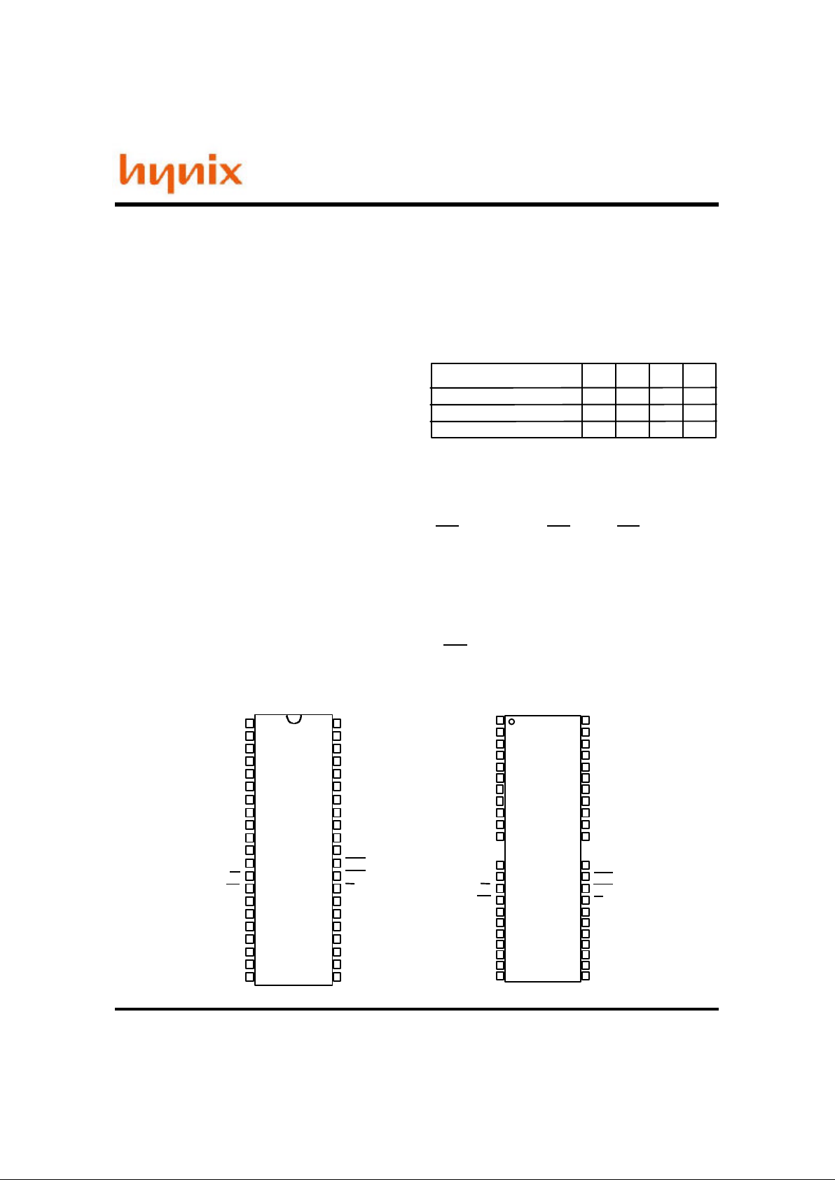
the GM71C(S)18163C/CL to be packaged in
standard 400 mil 42pin plastic SOJ, and standard
400mil 44(50)pin plastic TSOP II. The package
size provides high system bit densities and is
compatible with widely available automated
testing and insertion equipment.
Description Features
* 1,048,576 Words x 16 Bit Organization
* Extended Data Out Mode Capability
* Single Power Supply (5V+/-10%)
* Fast Access Time & Cycle Time
Pin Configuration
1,048,576 WORDS x 16 BIT
CMOS DYNAMIC RAM
GM71CS18163CL
(Unit: ns)
GM71C(S)18163C/CL-5
GM71C(S)18163C/CL-6
GM71C(S)18163C/CL-7
tRAC tCAC tRC tHPC
50601315 84
1042025
70 18 124 30
* Low Power
Active : 1045/935/825mW (MAX)
Standby : 11mW (CMOS level : MAX)
0.83mW (L-version : MAX)
* RAS Only Refresh, CAS before RAS Refresh,
Hidden Refresh Capability
* All inputs and outputs TTL Compatible
* 1024 Refresh Cycles/16ms
* 1024 Refresh Cycles/128ms (L-version)
* Self Refresh Operation (L-version)
* Battery Back Up Operation (L-version)
* 2 CAS byte Control
(Top View)
GM71C18163C
42
43
44
45
46
40
41
33
30
31
32
27
28
29
26
34
35
36
47
48
49
50
NC
NC
VSS
I/O15
I/O14
I/O13
I/O12
I/O11
I/O10
I/O9
I/O8
VSS
LCAS
UCAS
OE
A8
A7
A6
A5
A4
VSS
A9
VSS
I/O15
I/O14
I/O13
I/O12
38
39
40
41
42
I/O11
I/O10
I/O9
I/O8
NC
32
33
34
35
36
VSS
37
LCAS
UCAS
OE
29
30
31
A9
A8
A726
27
28
A6
A5
A423
24
25
VSS
22
11
1
2
3
4
5
7
8
9
10
6
15
16
17
18
19
20
21
22
23
24
25
NC
NC
I/O0
I/O1
I/O2
I/O3
I/O4
I/O5
I/O6
I/O7
VCC
NC
WE
RAS
A11
A10
A0
A1
VCC
VCC
A2
A3
44(50) TSOP II
VCC
I/O0
I/O1
I/O2
I/O3
1
2
3
4
5
I/O4
I/O5
I/O6
I/O7
NC
7
8
9
10
11
VCC
6
NC
WE
RAS
12
13
14
NC
NC
A0
15
16
17
A1
A2
A3
18
19
20
VCC
21
42 SOJ
Rev 0.1 / Apr’ 01
Page 2
GM71CS18163CL
GM71C18163C
Rev 0.1 / Apr’ 01
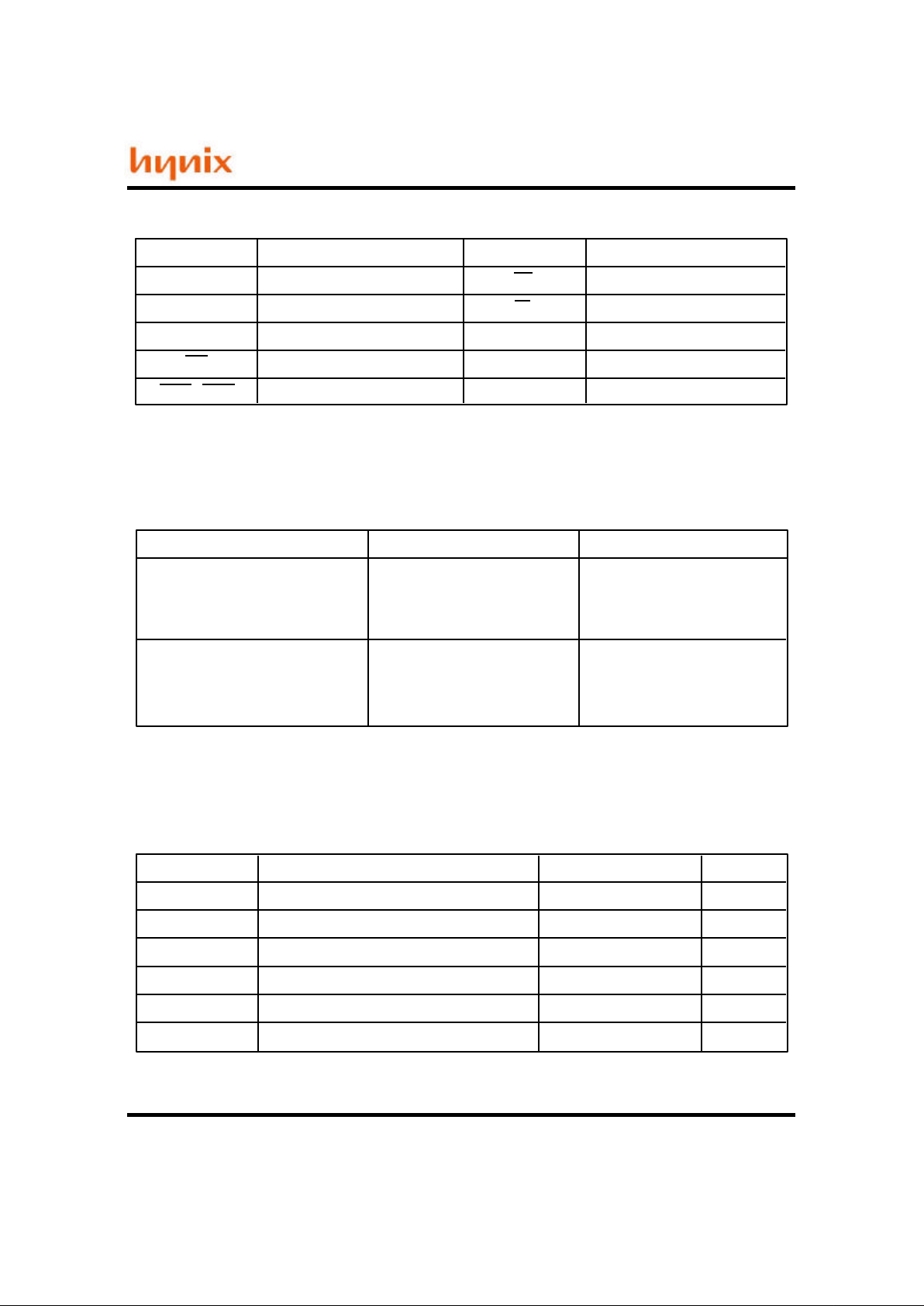
Pin Description
Pin Function Pin Function
A0-A9
A0-A9
I/O0-I/O15
RAS
WE
VCC
VSS
NC
Address Inputs
Refresh Address Inputs
Data Input/Data Output
Row Address Strobe
Read/Write Enable
Power (+5V)
Ground
No Connection
Ordering Information
UCAS, LCAS Column Address Strobe
OE Output Enable
Absolute Maximum Ratings*
PD 1.0
Power Dissipation
W
Symbol Parameter Rating Unit
TA
TSTG
VIN/OUT
VCC
IOUT
0 ~ +70
-55 ~ +125
50
Ambient Temperature under Bias
Storage Temperature
Voltage on any Pin Relative to VSS
Supply voltage Relative to VSS
Short Circuit Output Current
C
C
V
V
mA
-1.0 ~ +7.0V
-1.0 ~ +7.0V
Type No. Access Time Package
GM71C(S)18163CJ/CLJ -5
GM71C(S)18163CJ/CLJ -6
GM71C(S)18163CJ/CLJ -7
50ns
60ns
70ns
400 Mil
42 Pin
Plastic SOJ
50ns
60ns
70ns
400 Mil
44(50) Pin
Plastic TSOP II
GM71C(S)18163CT/CLT -5
GM71C(S)18163CT/CLT -6
GM71C(S)18163CT/CLT -7
Note: Operation at or above Absolute Maximum Ratings can adversely affect device reliability.
Page 3
GM71CS18163CL
GM71C18163C
Rev 0.1 / Apr’ 01
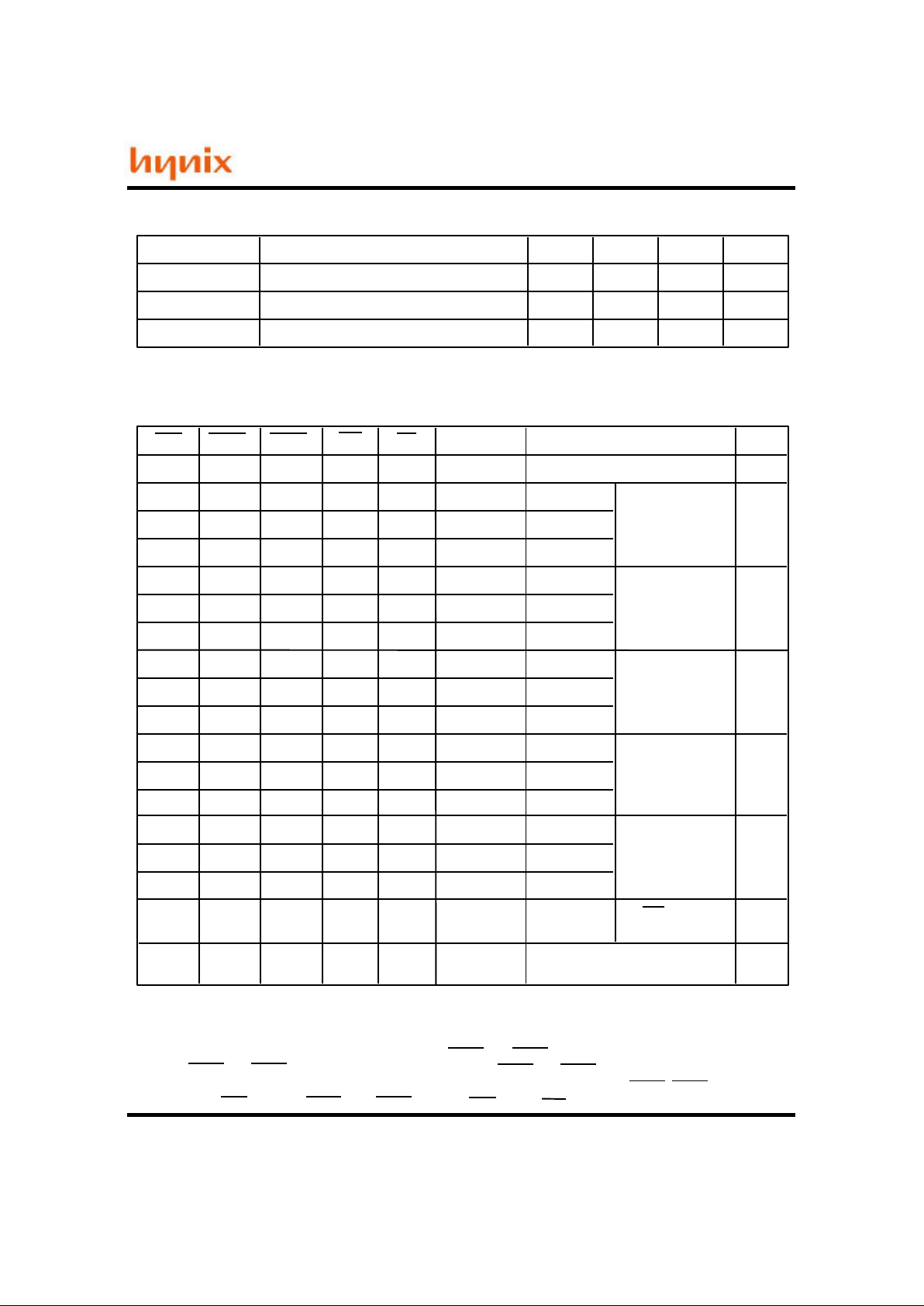
Truth Table
Notes: 1. H: High (inactive) L: Low(active) D: H or L
2. tWCS >= 0ns Early write cycle
tWCS <= 0ns Delayed write cycle
3. Mode is determined by the OR function of the UCAS and LCAS. (Mode is set by earliest of
UCAS and LCAS active edge and reset by the latest of UCAS and LCAS inactive edge.) However
write OPERATION and output High-Z control are done independently by each UCAS,LCAS.
ex) if RAS = H to L, UCAS = H, LCAS = L, then CAS-before-RAS refresh cycle is selected.
RAS LCAS UCAS WE OE
H
L
L
L
D
H
L
H
D
H
H
L
D
H
H
H
D
D
L
L
Output
Open
Valid
Valid
Valid
Lower byte
Upper byte
Word
Operation
Standby
RAS-only
Refresh cycle
Read cycle
L
L L
L
L
L H L
H
Early write cycle
L
H
L
L
H
Open
Open
Open
L
L
L
L
Undefined
Delayed Write
cycle
L
L
L
H
H
H to L
L
CBR Refresh
or
Self Refresh
(L-series)
H to L
H
L
H to L
L
L
Notes
1,3
1,3
1,3
1,3
1,3
1,2,3
1,2,3
1,3
Lower byte
Upper byte
Word
Lower byte
Upper byte
Word
Lower byte
Upper byte
Word
Undefined
Undefined
Open
Open
Open
Open
Open
Valid
Valid
Valid
Word
Word
Word
Word
Read-modify
-write cycle
Read cycle
(Output disabled)
D
D
H to L
H to L
H to L
L
L
L
L
L
L
L
H
L
L
L
L
H DD
L
H H
H
H
L
D
D
DD
DD
L to H
L to H
L to H
L
L
LL
Recommended DC Operating Conditions (TA = 0 ~ +70C)
Symbol Parameter Unit
VCC
VIH
VIL
Supply Voltage
Input High Voltage
Input Low Voltage
V
V
V
Max
5.5
6.0
0.8
Typ
5.0
-
-
Min
4.5
2.4
-1.0
Note: All voltage referred to Vss.
The supply voltage with all VCC pins must be on the same level. The supply voltage with all VSS pins must be
on the same level.
Page 4
GM71CS18163CL
GM71C18163C
Rev 0.1 / Apr’ 01
DC Electrical Characteristics (VCC = 5V+/-10%, Vss = 0V, TA = 0 ~ 70C)
Symbol Parameter Note
VOH
VOL
Output Level
Output "H" Level Voltage (IOUT = -2mA)
Unit
V
V
Max
VCC
0.4
Min
2.4
0
Output Level
Output "L" Level Voltage (IOUT = 2mA)
ICC1
Operating Current
Average Power Supply Operating Current
(RAS, UCAS or LCAS Cycling: tRC = tRC min)
ICC2 Standby Current (TTL)
Power Supply Standby Current
(RAS, UCAS, LCAS = VIH, DOUT = High-Z)
ICC3 RAS Only Refresh Current
Average Power Supply Current
RAS Only Refresh Mode
(tRC = tRC min)
ICC4
ICC5
Standby Current (CMOS)
Power Supply Standby Current
(RAS, UCAS or LCAS >=VCC - 0.2V, DOUT = High-Z)
ICC6
CAS-before-RAS Refresh Current
(tRC = tRC min)
ICC7
IL(I)
uA10-10
IL(O)
uA10-10
Input Leakage Current
Any Input (0V<=VIN<= 6V)
Output Leakage Current
(DOUT is Disabled, 0V<=VOUT<= 6V)
EDO Page Mode Current
Average Power Supply Current
EDO Page Mode
(tHPC = tHPC min)
Note: 1. ICC depends on output load condition when the device is selected.
ICC(max) is specified at the output open condition.
2. Address can be changed once or less while RAS = VIL.
3. Address can be changed once or less while UCAS and LCAS = VIH.
4. CAS = L (<=0.2V) while RAS = L (<=0.2V).
5. L-version.
Battery Back Up Operating Current(Standby with CBR Ref.)
(CBR refresh, tRC=125us, tRAS<=0.3us,
DOUT=High-Z, CMOS interface)
500- 4,5uA
ICC8
ICC9
uA
Self-Refresh Mode Current
(RAS, UCAS or LCAS <=0.2V, DOUT=High-Z, CMOS interface)
300-
5
mA
2-
mA1
150
-
uA
mA
190-50ns
60ns
70ns
170
150
-
1, 2
-
mA 2
mA 1, 3
-
190-50ns
60ns
70ns
170
150
-
-
-
185-50ns
60ns
70ns
165
145
-
mA
190-50ns
60ns
70ns
-
-
170
150
5
-
Standby Current RAS = VIH
UCAS, LCAS = VIL
DOUT = Enable
5 1
mA
Page 5

GM71CS18163CL
GM71C18163C
Rev 0.1 / Apr’ 01
Read, Write, Read-Modify-Write and Refresh Cycles (Common Parameters)
Symbol Parameter
Note
Max
Unit
Min MaxMin MaxMin
tRC
Random Read or Write Cycle Time 84 - 104 - 124 -
tRP
RAS Precharge Time 30 - 40 - 50 -
tRAS
RAS Pulse Width 50 10,000
60
10,000
70
10,000
tCAS
CAS Pulse Width 7 10,000 10,000 10,00010 13
tASR
Row Address Set up Time 0 - - -0 0
tRAH
Row Address Hold Time 7 - - -10 10
tASC
Column Address Set-up Time 0 - - -0 0
tCAH
Column Address Hold Time 7 - - -10 13
tRCD RAS to CAS Delay Time 11 37 45 5214 14 3
tRAD
RAS to Column Address Delay Time 9 25 30 3512 12 4
tRSH RAS Hold Time 10 - - -13 13
tCSH CAS Hold Time 35 - - -40 45
tCRP
CAS to RAS Precharge Time 5 - - -5 5
tT
Transition Time (Rise and Fall) 2 50 50 502 2 7
Capacitance (VCC = 5V+/-10%, TA = 25C)
Symbol Parameter Note
CI1
CI2
CI/O
Input Capacitance (Address)
Input Capacitance (Clocks)
Output Capacitance (Data-In/Out)
1
1
1, 2
Unit
pF
Max
5
7
7
Min
-
-
-
Note: 1. Capacitance measured with Boonton Meter or effective capacitance measuring method.
2. LCAS and UCAS = VIH to disable DOUT.
AC Characteristics (VCC = 5V+/-10%, TA = 0 ~ +70C, Note 1, 2, 18, 19, 20)
tDZO OE Delay Time from DIN 0 - - -0 0
tDZC CAS Delay Time from DIN 0 - - -0 0
GM71C(S)18163
C/CL-5
OE to DIN Delay Time 13 - - -15 18 5
6
6
tCP CAS Precharge Time 7 - 10 - 13 -
tODD
Test Conditions
Input rise and fall times : 2 ns Output timing reference levels : 0.8V, 2.0V
Input levels : VIL = 0V, VIH = 3V Output load : 1TTL gate + CL (100 pF)
Input timing reference levels : 0.8V, 2.4V (Including scope and jig)
GM71C(S)18163
C/CL-6
GM71C(S)18163
C/CL-7
ns
ns
ns
ns
ns
ns
ns
ns
ns
ns
ns
ns
ns
ns
ns
ns
ns
ns
pF
pF
21
21
22
23
Page 6

GM71CS18163CL
GM71C18163C
Rev 0.1 / Apr’ 01
Read Cycle
Symbol Parameter
Note
Max
Unit
Min MaxMin
tRAC
Access Time from RAS - 60 - 70
tCAC
Access Time from CAS - 15 - 18
tAA
Access Time from Address - 30 - 35
tRCS
Read Command Setup Time 0 -
0
-
tRCH
Read Command Hold Time to CAS 0 - -0
8,9
9,10,17
9,11,17
- 15 - 18 9
12,22
Access Time from OE
GM71C(S)18163
C/CL-6
tOAC
GM71C(S)18163
C/CL-7
tRRH
Read Command Hold Time to RAS 5
- -
5 12
tRAL
Column Address to RAS Lead Time 30
-
-35
tOFF
Output Buffer Turn-off Time 15 15 13,27
-
-
tCAL
Column Address to CAS Lead Time 18 - -23
tCLZ
CAS to Output in Low-Z 0 -
-
0
tOEZ
Output Buffer Turn-off Time to OE 15 15 13
-
-
tOH
Output Data Hold Time 3 -
-
3
tOHO
Output Data Hold Time from OE 3 -
-
3
tCDD
CAS to DIN Delay Time
15
-
-18
5
tRCHR
tOHR
tOFR
tWEZ
tWDD
tRDD
Read Command Hold Time from RAS
60
70
Output Data hold Time from RAS
3
3
Output Buffer turn off to RAS
Output Buffer turn off to WE
WE to DIN Delay Time
RAS to DIN Delay Time
15
15
15
15
18
18
-
-
-
-
-
-
-
-
-
-
-
-
MaxMin
- 50
- 13
- 25
0 0 -
- 13
GM71C(S)18163
C/CL-5
5
-
25 -
13
-
15
-
0 -
13-
3 3 -
13 50
3
13
13
13
-
-
-
-
-
-
ns
ns
ns
ns
ns
ns
ns
ns
ns
ns
ns
ns
ns
ns
ns
ns
ns
ns
ns
ns
ns
13 15 15
21
27
27
27
Page 7

GM71CS18163CL
GM71C18163C
Rev 0.1 / Apr’ 01
Write Cycle
Symbol Parameter
Note
Max
Unit
Min MaxMin
tWCS
Write Command Setup Time
0 - 0 -
tWCH
Write Command Hold Time 10
-
13
-
tWP
Write Command Pulse Width 10
-
10
-
tRWL
Write Command to RAS Lead Time 10
-
13
-
tCWL
Write Command to CAS Lead Time 10
- -
13
tDS
Data-in Setup Time
0 - -0
tDH
Data-in Hold Time 10
- -
13 15,23
15,23
14,21
GM71C(S)18163
C/CL-6
GM71C(S)18163
C/CL-7
Read- Modify-Write Cycle
Symbol Parameter
Max
NoteUnit
Min MaxMin
tRWC Read-Modify-Write Cycle Time 136 - 161 -
tRWD RAS to WE Delay Time 79 - 92 -
tCWD CAS to WE Delay Time 34 - 40 -
tAWD Column Address to WE Delay Time 49 - 57 - 14
14
14
tOEH OE Hold Time from WE 15 - 18 -
GM71C(S)18163
C/CL-6
GM71C(S)18163
C/CL-7
ns
Min
0 -
7
-
7
-
-
-
0 -
-
Max
GM71C(S)18163
C/CL-5
7
7
7
ns
ns
ns
ns
ns
ns
ns
ns
ns
ns
ns
Min
111 -
67 30 42 13 -
Max
GM71C(S)18163
C/CL-5
21
23
Refresh Cycle
Symbol Parameter
Note
Max
Unit
Min MaxMin
tCSR CAS Setup Time
(CAS-before-RAS Refresh Cycle)
5 - 5 - ns
tCHR CAS Hold Time
(CAS-before-RAS Refresh Cycle)
10 - 10 - ns
tRPC
RAS Precharge to CAS Hold Time 5 - 5 - ns
GM71C(S)18163
C/CL-6
GM71C(S)18163
C/CL-7
Min
5 -
7 -
5 -
GM71C(S)18163
C/CL-5
Max
21
22
21
Page 8

GM71CS18163CL
GM71C18163C
Rev 0.1 / Apr’ 01
Symbol Parameter
Note
Max
Unit
Min MaxMin
tHPC
25 - 30 -
tRASP
tACP
Access Time from CAS Precharge
35 - 40 -
tRHCP
RAS Hold Time from CAS Precharge
9,17,22- -
16EDO Page Mode RAS Pulse Width
100,000 100,000
- 35 40
GM71C(S)18163
C/CL-6
GM71C(S)18163
C/CL-7
EDO Page Mode Cycle
EDO Page Mode Cycle Time 25
tDOH
tCOL
tCOP
tRCHP
Output data Hold Time from CAS low
3 3-
-
-
-
9
CAS Hold Time referred OE
10 13
CAS to OE Setup Time
5 5
Read command Hold Time
from CAS Precharge
35
40
ns
ns
ns
ns
ns
ns
ns
ns
Min
20 -
30 -
-
-
GM71C(S)18163
C/CL-5
3 -
-
-
-
5
30
Max
100,000
7
30
EDO Page Mode Read-Modify-Write Cycle
Symbol Parameter
Note
Max
Unit
Min MaxMin
tHPRWC EDO Page Mode Read-Modify-Write
Cycle Time
68 - 79 - ns
tCPW
WE Delay Time from CAS Precharge
54 - 62 -
ns
14,22
GM71C(S)18163
C/CL-6
GM71C(S)18163
C/CL-7
Refresh
Symbol Parameter
Note
Max
Unit
Min MaxMin
tREF Refresh period
16
-
-
ms
tREF
Refresh period (L -Series) 128- 128
- ms
GM71C(S)18163
C/CL-6
GM71C(S)18163
C/CL-7
16
1024
cycles
1024
cycles
MaxMin
57 -
45 -
GM71C(S)18163
C/CL-5
MaxMin
16
-
128-
GM71C(S)18163
C/CL-5
Page 9

GM71CS18163CL
GM71C18163C
Rev 0.1 / Apr’ 01
Self Refresh Mode ( L-version )
Symbol Parameter Note
Max
Unit
Min MaxMin
tRASS
RAS Pulse Width(Self-Refresh) 100
-
100
-
tRPS
RAS Precharge Time(Self-Refresh)
110
-
130
-
ns
tCHS
CAS Hold Time(Self-Refresh) -50
-
-50
-
ns
GM71CS18163
CL-6
GM71CS18163
CL-7
us
MaxMin
100
-
90
-
-50
-
GM71CS18163
CL-5
29
1. AC measurements assume tT = 2 ns.
2. An initial pause of 200us is required after power followed by a minimum of eight initializa tion cycles (any combination of cycles containing RAS-only refresh or CAS-before-RAS
refresh).
3. Operation with the tRCD (max) limit insures that tRAC (max) can be met, tRCD (max) is
specified as a reference point only; if tRCD is greater than the specified tRCD (max) limit, then
access time is controlled exclusively by tCAC.
4. Operation with the tRAD (max) limit insures that tRAC (max) can be met, tRAD (max) is
specified as a reference point only; if tRAD is greater than the specified tRAD (max) limit, then
access time is controlled exclusively by tAA.
5. Either tODD or tCDD must be satisfied.
6. Either tDZO or tDZC must be satisfied.
7. VIH (min) and VIL (max) are reference levels for measuring timing of input signals. Also,
transition times are measured between VIH (min) and VIL (max).
8. Assumes that tRCD <= tRCD (max) and tRAD <= tRAD (max). If tRCD or tRAD is greater than the
maximum recommended value shown in this table, tRAC exceeds the value shown.
9. Measured with a load circuit equivalent to 1TTL loads and 100pF.
10. Assumes that tRCD >= tRCD (max) and tRAD <= tRAD (max).
11. Assumes that tRCD <= tRCD (max) and tRAD >= tRAD (max).
12. Either tRCH or tRRH must be satisfied for a read cycles.
13. tOFF (max) and tOEZ (max) define the time at which the outputs achieve the open circuit condi tion and are not referred to output voltage levels.
14. tWCS, tRWD, tCWD, tAWD and tCPW are not restrictive operating parameters. They are included in
the data sheet as electrical characteristics only; if tWCS >= tWCS (min), the cycle is an early
write cycle and the data out pin will remain open circuit(high impedance) throughout the
entire cycle; if tRWD>=tRWD(min), tCWD>=tCWD(min), and tAWD>=tAWD(min), or tCWD>=tCWD(min)
tAWD >= tAWD (min) and tCPW >= tCPW (min), the cycle is a read-modify-write and the data out put will contain data read from the selected cell; if neither of the above sets of conditions is
satisfied, the condition of the data out (at access time) is indeterminate.
Notes :
Page 10

GM71CS18163CL
GM71C18163C
Rev 0.1 / Apr’ 01
15. These parameters are referred to UCAS and LCAS leading edge in early write cycles and to
WE leading edge in delayed write or read-modify-write cycles.
16. tRASP defines RAS pulse width in EDO mode cycles.
17. Access time is determined by the longer of tAA or tCAC or tACP.
18. In delayed write or read-modify-write cycles, OE must disable output buffer prior to applying
data to the device. After RAS is reset, if tOEH>=tCWL, the I/O pin will remain open circuit (high
impedance): if tOEH<=tCWL, invalid data will be out at each I/O.
19. When both LCAS and UCAS go low at the same time, all 16-bits data are written into the
device. LCAS and UCAS cannot be staggered within the same write/read cycles.
20. All the Vcc and Vss pins shall be supplied with the same voltages.
21. tASC, tCAH, tRCS, tWCS, tWCH, tCSR and tRPC are determined by the earlier falling edge of UCAS
or LCAS.
22. tCRP, tCHR, tRCH, tACP and tCPW are determined by the later rising edge of UCAS or LCAS.
23. tCWL, tDH, tDS and tCHS should be satisfied by both UCAS and LCAS.
24. tCP is determined by the time that both UCAS and LCAS are high.
tHPC(min) can be achieved during a series of EDO page made write cycles or EDO mode
write cycles. It both write and read operation are mixed in a EDO mode RAS cycle(EDO
mode mix cycle (1),(2)) minimum Value of CAS cycle (tCAS+tCP+2tT) becomes greater than
the specified tHPC (min) value. The value of CAS cycle time of mixed EDO mode is shown
in EDO mode mix cycle (1) and (2).
When output buffers are enabled once, sustain the low impedance state until valid data
is obtained. When output buffer is turned on and off within a very short time , generally
it causes large Vcc/Vss line noise, which causes to degrade VIH min/VIL max level.
Data output turns off and becomes high impedance from later rising edge of RAS and CAS.
Hold time and turn off time are specified by the timing specification of later rising edge of
RAS and CAS between tOHR and tOH, and between tOFR and tOFF.
EDO Hi-Z control by OE or WE. OE rising edge disables data outputs. When OE goes high
during CAS high, the data will not come out until next CAS access. When WE goes low
during CAS high, the data will not come out until next CAS access.
Please do not use tRASS timing, 10us<=tRASS<=100us. During this period, the device is in
transition state from normal operation mode to self refresh mode. If tRASS>=100us, then
RAS
precharge time should use tRPS instead of tRP.
25.
26.
29.
27.
28.
H or L ( H : VIH(min) <= VIN <= VIH(max), L : VIL(min) <= VIN <= VIL(max) )
30.
Page 11

GM71CS18163CL
GM71C18163C
Rev 0.1 / Apr’ 01
Package Dimension
42 SOJ
Unit: Inches (mm)
0.405(10.29) MAX
0.394(10.03) MIN
0.455(11.56) MIN
0.471(11.96) MAX
0.017(0.45) MAX
0.012(0.30) MIN
TYP
0.031(0.80)
0.830(21.08) MAX
0.820(20.82) MIN
0.047(1.20)
MAX
0.006(0.15) MAX
0.002(0.05) MIN
0.041(1.05) MAX
0.037(0.95) MIN
0.024(0.60) MAX
0.016(0.40) MIN
0.008(0.21) MAX
0.004(0.12) MIN
0 ~ 5
¡£
1.072(27.23) MAX
0.395(10.03) MIN
0.435(11.06) MIN
0.445(11.30) MAX
0.148(3.75) MAX
0.128(3.25) MIN
0.026(0.66) MIN
TYP
0.050(1.27)
0.405(10.29) MAX
0.020(0.50) MAX
0.015(0.38) MIN
1.058(26.89) MAX
0.360(9.15) MIN
0.380(9.65) MAX
0.025(0.64)
MIN
0.093(2.38)
MIN
0.032(0.81) MAX
44(50) TSOP-II
 Loading...