

Datasheet GM71C17400CLJ-7, GM71C17400CLJ-6, GM71C17400CLJ-5, GM71C17400CJ-7, GM71C17400CJ-5 Datasheet (HYNIX)
...Page 1
GM71C(S)17400C/CL
4,194,304 WORDS x 4 BIT
CMOS DYNAMIC RAM
Description
The GM71C(S)17400C/CL is the new
generation dynamic RAM organized 4,194,304
words x 4 bit. GM71C(S)17400C/CL has
realized higher density, higher performance and
various functions by utilizing advanced CMOS
process technology. The GM71C(S)17400C/CL
offers Fast Page Mode as a high speed access
mode. Multiplexed address inputs permit the
GM71C(S)17400C/CL to be packaged in a
standard 300 mil 24(26) pin SOJ, and a standard
300 mil 24(26) pin plastic TSOP II. The
package size provides high system bit densities
and is compatible with widely available
automated testing and insertion equipment.
System oriented features include single power
supply 5.0V+/-10% tolerance, direct interfacing
capability with high performance logic families
such as Schottky TTL.
Features
* 4,194,304 Words x 4 Bit Organization
* Fast Page Mode Capability
* Single Power Supply (5.0V+/-10%)
* Fast Access Time & Cycle Time
* Low Power
Active : 660/605/550mW (MAX)
Standby : 11mW (CMOS level : MAX)
: 0.83mW (L-version : MAX)
* RAS Only Refresh, CAS before RAS Refresh,
Hidden Refresh Capability
* All inputs and outputs TTL Compatible
* 2048 Refresh Cycles/32ms
* 2048 Refresh Cycles/128ms (L-version)
* Battery backup operation (L-version)
* Test function : 16bit parallel test mode
(Unit: ns)
GM71C(S)17400C/CL-5
GM71C(S)17400C/CL-6
GM71C(S)17400C/CL-7
tRAC tCAC tRC tPC
5060131590
1103540
70 18 130 45
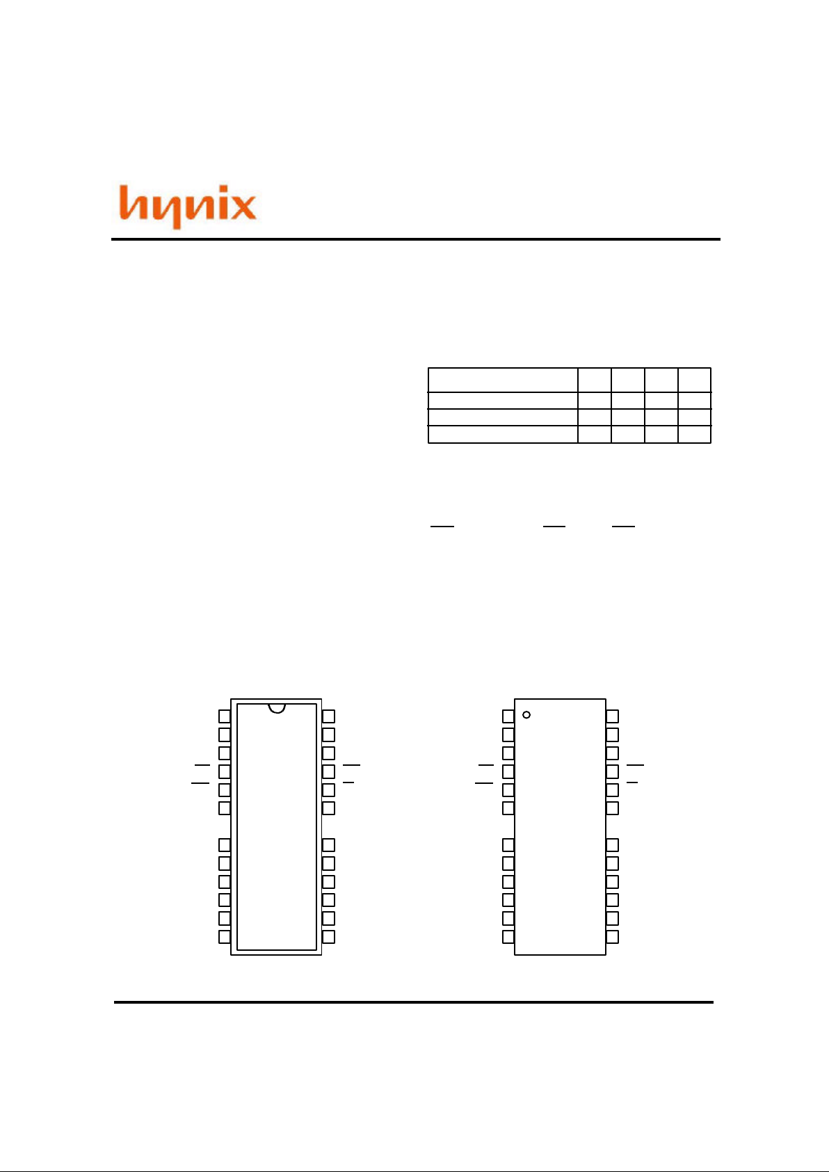
Pin Configuration
24(26) SOJ
(Top View)
VCC
I/O1
I/O2
WE
RAS
NC
A10
A0
A1
A2
A3
VCC
VSS
I/O4
I/O3
CAS
OE
A9
A8
A7
A6
A5
A4
VSS
1
2
3
4
5
6
8
9
10
11
12
13 14
15
16
17
18
19
21
22
23
24
25
26
24(26) TSOP II
VCC
I/O1
I/O2
WE
RAS
A11
A10
A0
A1
A2
A3
VCC
VSS
I/O4
I/O3
CAS
OE
A9
A8
A7
A6
A5
A4
VSS
1
2
3
4
5
6
8
9
10
11
12
13 14
15
16
17
18
19
21
22
23
24
25
26
Rev 0.1 / Apr’ 01
Page 2
GM71C(S)17400C/CL
Rev 0.1 / Apr’ 01
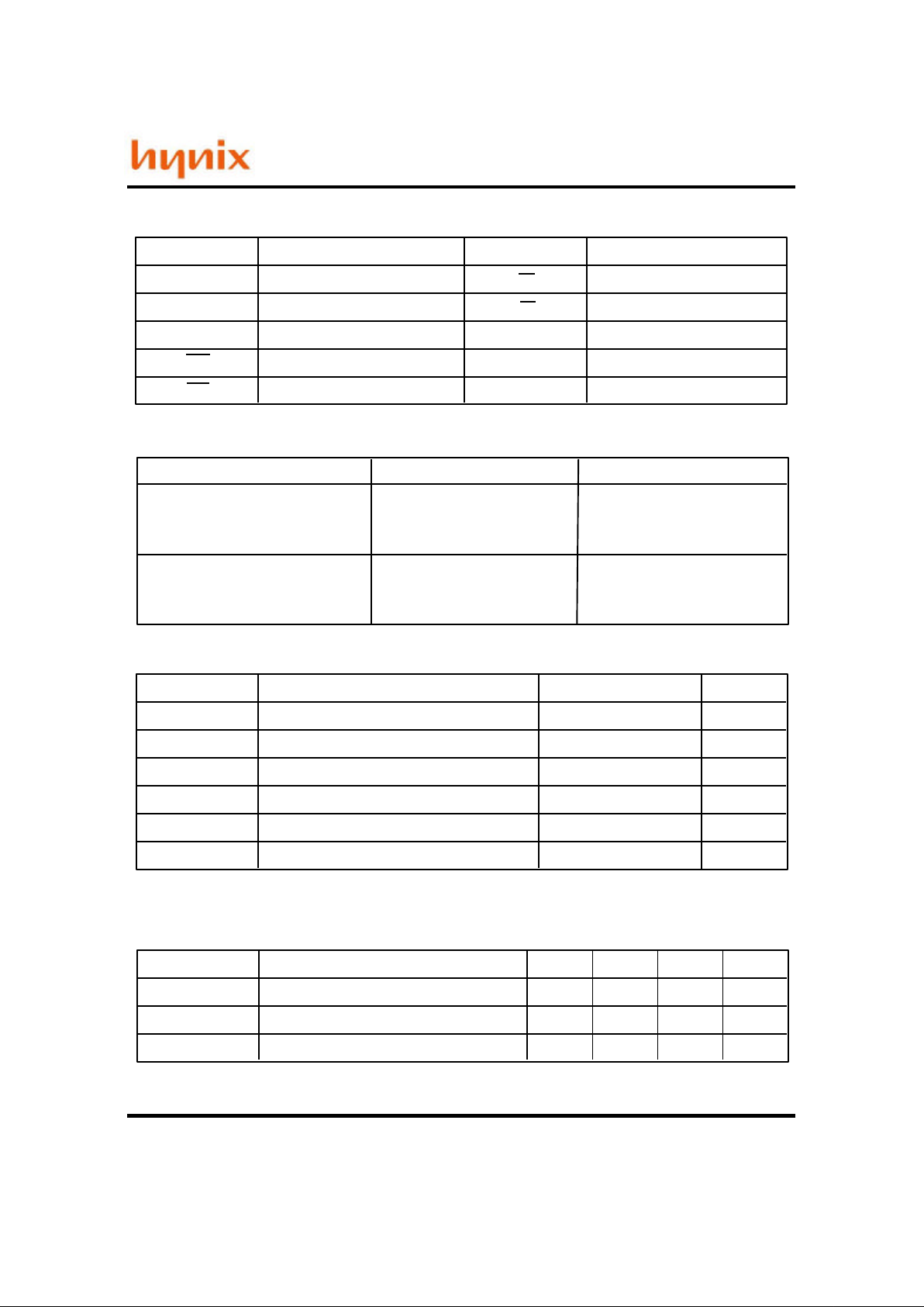
Pin Description
Pin Function Pin Function
A0-A10
A0-A10
I/O1-I/O4
VCC
VSS
Address Inputs
Refresh Address Inputs
Data Input/Data Output
Row Address Strobe
Column Address Strobe
Read/Write Enable
Output Enable
Power (5.0V)
Ground
Ordering Information
Type No. Access Time Package
GM71C(S)17400CJ/CLJ-5
GM71C(S)17400CJ/CLJ-6
GM71C(S)17400CJ/CLJ-7
50ns
60ns
70ns
300 Mil
24(26) Pin
Plastic SOJ
GM71C(S)17400CT/CLT-5
GM71C(S)17400CT/CLT-6
GM71C(S)17400CT/CLT-7
50ns
60ns
70ns
300 Mil
24(26) Pin
Plastic TSOP II
Absolute Maximum Ratings*
Note: All voltage referred to Vss.
RAS
CAS
Recommended DC Operating Conditions (TA = 0 ~ 70C)
OE
NC No Connection
WE
Symbol Parameter Rating Unit
TA
TSTG
VIN/VOUT
VCC
IOUT
0 ~ 70
-55 ~ 125
-1.0 ~ 7.0
-1.0 ~ 7.0
50
Ambient Temperature under Bias
Storage Temperature (Plastic)
Voltage on any Pin Relative to VSS
Voltage on VCC Relative to VSS
Short Circuit Output Current
V
V
mA
PD
1.0Power Dissipation W
*Note: Operation at or above Absolute Maximum Ratings can adversely affect device reliability.
C
C
Symbol Parameter Unit
VCC
VIH
VIL
Supply Voltage
Input High Voltage
Input Low Voltage
V
V
V
Max
5.5
6.0
0.8
Typ
5.0
-
-
Min
4.5
2.4
-1.0
Page 3
GM71C(S)17400C/CL
Rev 0.1 / Apr’ 01
DC Electrical Characteristics (VCC = 5.0V+/-10%, Vss = 0V, TA = 0 ~ 70C)
Symbol Parameter Note
VOH
VOL
Output Level
Output "H" Level Voltage (IOUT = -5mA)
UnitMax
VCC
0.4
Min
2.4
0
Output Level
Output "L" Level Voltage (IOUT = 4.2mA)
ICC1
Operating Current
Average Power Supply Operating Current
(RAS, CAS Cycling : tRC = tRC min)
ICC2 Standby Current (TTL)
Power Supply Standby Current
(RAS, CAS = VIH, DOUT = High-Z)
ICC3 RAS Only Refresh Current
Average Power Supply Current
RAS Only Refresh Mode
(tRC = tRC min)
ICC4
ICC5 Standby Current (CMOS)
Power Supply Standby Current
(RAS, CAS >= VCC - 0.2V, DOUT = High-Z)
1-
ICC6 CAS-before-RAS Refresh Current
(tRC = tRC min)
150-
ICC8
IL(I)
10-10
IL(O)
10-10
Input Leakage Current
Any Input (0V<=VIN<= 6V)
Output Leakage Current
(DOUT is Disabled, 0V<=VOUT<= 6V)
Note: 1. ICC depends on output load condition when the device is selected.
ICC(max) is specified at the output open condition.
2. Address can be changed once or less while RAS = VIL.
3. Address can be changed once or less while CAS = VIH.
4. L-version.
Fast Page Mode Current
Average Power Supply Current
Fast Page Mode
(tPC = tPC min)
2-
100-50ns
60ns
70ns
90
80
-
-
-
100-50ns
60ns
70ns
90
80
-
-
90-50ns
60ns
70ns
80
70
-
V
V
mA
uA
uA
ICC7
- 5
Standby Current RAS = VIH
CAS = VIL
DOUT = Enable
1mA
Battery Backup Operating Current(Standby with CBR Refresh)
(CBR refresh, tRC=62.5us, tRAS<=0.3us,
DOUT=High-Z, CMOS interface)
350- uA 4
uA
4
mA
mA 1, 2
mA 2
mA 1, 3
mA
-
100-50ns
60ns
70ns
90
80
-
Page 4

GM71C(S)17400C/CL
Rev 0.1 / Apr’ 01
Capacitance (VCC = 5.0V+/-10%, TA = 25C)
AC Characteristics (VCC = 5.0V+/-10%, Vss=0V, TA = 0 ~ 70C, Notes 1, 2, 18,19)
Read, Write, Read-Modify-Write and Refresh Cycles (Common Parameters)
Symbol Parameter Note
CI1
CI2
CI/O
Input Capacitance (Address)
Input Capacitance (Clocks)
Output Capacitance (Data-In/Out)
1
1
1, 2
Unit
pF
pF
pF
Max
5
7
7
Min
-
-
-
Input rise and fall times : 5ns
Input timing reference levels : 0.8V, 2.4V
Output timing reference levels : 0.4V, 2.4V
Output load : 2 TTL gate + CL (100pF)
(Including scope and jig)
Note: 1. Capacitance measured with Boonton Meter or effective capacitance measuring method.
2. CAS = VIH to disable DOUT.
Test Conditions
Symbol Parameter
Note
Max
Unit
Min MaxMin MaxMin
tRC
90 - 110 - 130 -
tRP
30 - 40 - 50 -
tRAS 50 10,000
60
10,000
70
10,000
tCAS 10,000 10,000 10,00015 18
tASR 0 - - -0 0
tRAH 7 - - -10 10
tASC 0 - - -0 0
tCAH - - -10 15
tRCD
17 45 45 5220 20 3
tRAD 12 30 30 3515 15 4
tRSH 13 - - -15 18
tCSH
50 - - -60 70
tCRP
5 - - -5 5
tT 3 50 50 503 3 7
tDZO 0 - - -0 0
tDZC
0 - - -0 0
GM71C(S)17400
C/CL-5
13 - - -15 18 5
6
6
tCP
- 10 - 10 -
tODD
GM71C(S)17400
C/CL-6
GM71C(S)17400
C/CL-7
ns
ns
ns
ns
ns
ns
ns
ns
ns
ns
ns
ns
ns
ns
ns
ns
ns
ns
13
7
7
Random Read or Write Cycle Time
Row Address Set up Time
Row Address Hold Time
Column Address Set-up Time
Column Address Hold Time
RAS Hold Time
Transition Time (Rise and Fall)
RAS Precharge Time
RAS to CAS Delay Time
RAS to Column Address Delay Time
CAS Hold Time
CAS to RAS Precharge Time
OE Delay Time from DIN
CAS Delay Time from DIN
OE to DIN Delay Time
CAS Precharge Time
RAS Pulse Width
CAS Pulse Width
Page 5

GM71C(S)17400C/CL
Rev 0.1 / Apr’ 01
Read Cycle
Write Cycle
Symbol Parameter
MaxMin MaxMin
- 60 - 70
- 15 - 18
- 30 - 35
0 - 0 0 - -0
5 - -5
30 - -35
0 - -0
30 - -35
- 15 15-
- 15 - 18
3 - -3
3 - -3
- 15 15-
15 - -18
Access Time from Address
Read Command Setup Time
Read Command Hold Time to CAS
Read Command Hold Time to RAS
Column Address to RAS Lead Time
Access Time from RAS
Access Time from CAS
CAS to Output in low-Z
Column Address to CAS Lead Time
Output Buffer Turn-off Time
Access Time from OE
Output Data Hold Time
Output Data Hold Time from OE
Output Buffer Turn-off Time to OE
CAS to DIN Delay Time
GM71C(S)17400
C/CL-6
GM71C(S)17400
C/CL-7
MaxMin
- 50
- 13
- 25
0 0 5 -
25 -
0 -
25 -
- 13
- 13
3 3 -
- 13
13 -
GM71C(S)17400
C/CL-5
Symbol Parameter
MaxMin MaxMin
0 - 0 -
10
-
15
-
10
-
10
-
15
-
18
-
15
- -
18
0 - -0
tRAC
tCAC
tAA
tRCS
tRCH
tRRH
tRAL
tCLZ
tCAL
tOFF
tOAC
tOH
tOHO
tOEZ
tCDD
tWCS
tWCH
tWP
tRWL
tCWL
tDS
tDH
Write Command Setup Time
Write Command Hold Time
Write Command Pulse Width
Data-in Setup Time
Data-in Hold Time 10
- -
15
Write Command to RAS Lead Time
Write Command to CAS Lead Time
GM71C(S)17400
C/CL-6
GM71C(S)17400
C/CL-7
Min
0 -
-
7
-
-
-
0 -
-
Max
GM71C(S)17400
C/CL-5
Unit
ns
ns
ns
ns
ns
ns
ns
ns
ns
ns
ns
ns
ns
ns
ns
Unit
ns
ns
ns
ns
ns
ns
ns
7
13
13
7
Note
12
12
8,9,20
9,11,
17,20
9,10,
17,20
13
9
13
5
15
15
14
Note
Page 6

GM71C(S)17400C/CL
Rev 0.1 / Apr’ 01
Read- Modify-Write Cycle
Refresh Cycle
Fast Page Mode Cycle
MaxMin MaxMin
155 - 181 -
85 - 98 40 - 46 55 - 63 15 - 18 -
Read-Modify-Write Cycle Time
Column Address to WE Delay Time
RAS to WE Delay Time
CAS to WE Delay Time
OE Hold Time from WE
GM71C(S)17400
C/CL-6
GM71C(S)17400
C/CL-7
Min
131 -
73 36 48 13 -
Max
GM71C(S)17400
C/CL-5
MaxMin MaxMin
5 - 5 -
10 - 10 -
5 - 5 -
GM71C(S)17400
C/CL-6
GM71C(S)17400
C/CL-7
0 - 0 -
10 - 10 -
CAS Setup Time
(CAS-before-RAS Refresh Cycle)
CAS Hold Time
(CAS-before-RAS Refresh Cycle)
RAS Precharge to CAS Hold Time
WE Setup Time
(CAS-before-RAS Refresh Cycle)
WE Hold Time
(CAS-before-RAS Refresh Cycle)
Min
5 -
7 -
5 -
GM71C(S)17400
C/CL-5
0 -
10 -
Max
Symbol
Symbol
Symbol
Parameter
Parameter
Parameter
MaxMin MaxMin
40 - 45 -
35 - 40 -
tRWC
tRWD
tCWD
tAWD
tOEH
tCSR
tCHR
tRPC
tWRP
tWRH
tPC
tRASP
tACP
tRHCP
Unit
ns
ns
ns
ns
ns
Unit
ns
ns
ns
ns
ns
Unit
ns
ns
ns
ns
- -
100,000 100,000
- 35 40
GM71C(S)17400
C/CL-6
GM71C(S)17400
C/CL-7
Access Time from CAS Precharge
RAS Hold Time from CAS Precharge
Fast Page Mode RAS Pulse Width
Fast Page Mode Cycle Time
Min
35 -
30 -
--30
GM71C(S)17400
C/CL-5
Max
100,000
Note
14
14
14
Note
Note
9,17,20
16
Page 7

GM71C(S)17400C/CL
Rev 0.1 / Apr’ 01
Test Mode Cycle
Fast Page Mode Read-Modify-Write Cycle
Refresh
Symbol Parameter
Unit
MaxMin MaxMin
- 32 -
Refresh Period
Refresh Period (L - version)
- 128 -
GM71C(S)17400
C/CL-6
GM71C(S)17400
C/CL-7
ms
ms
32
128
∗19
Symbol Parameter
Max
Unit
Min MaxMin
85 - 96 - ns
60 - 68 - ns
Fast Page Mode Read-Modify-Write
Cycle Time
WE Delay Time from CAS Precharge
GM71C(S)17400
C/CL-6
GM71C(S)17400
C/CL-7
GM71C(S)17400
C/CL-5
MaxMin
76 -
53 -
Symbol Parameter
Note
2048
cycles
2048
cycles
Note
14
Note
Max
Unit
Min MaxMin
GM71C(S)17400
C/CL-6
GM71C(S)17400
C/CL-7
0 - 0 - ns
10 - 10 - ns
Min
0 -
10 -
Max
GM71C(S)17400
C/CL-5
MaxMin
- 32
- 128
GM71C(S)17400
C/CL-5
tREF
tREF
tPRWC
tCPW
tWTS
tWTH
Test Mode WE Setup Time
Test Mode WE Hold Time
Page 8

GM71C(S)17400C/CL
Rev 0.1 / Apr’ 01
AC Measurements assume tT =5ns.
An initial pause of 200us is required after power up followed by a minimum of eight
initialization cycles (any combination of cycles containing RAS-only refresh or CAS-beforeRAS refresh). If the internal refresh counter is used, a minimum of eight CAS-before-RAS
refresh cycles are required.
Operation with the tRCD(max) limit insures that tRAC(max) can be met, tRCD(max) is specified as a
reference point only; if tRCD is greater than the specified tRCD(max) limit, then access time is
controlled exclusively by tCAC.
Operation with the tRAD(max) limit insures that tRAC(max) can be met, tRAD(max) is specified as a
reference point only; if tRAD is greater than the specified tRAD(max) limit, then access time is
controlled exclusively by tAA.
Either tODD or tCDD must be satisfied.
Either tDZO or tDZC must be satisfied.
VIH(min) and VIL(max) are reference levels for measuring timing of input signals. Also,
transition times are measured between VIH(min) and VIL(max).
Assume that tRCD<=tRCD(max) and tRAD<=tRAD(max). If tRCD or tRAD is greater than the maximum
recommended value shown in this table, tRAC exceeds the value shown.
Measured with a load circuit equivalent to 2 TTL loads and 100pF. (VOH = 2.4V, VOL = 0.8V)
Assume that tRCD >=tRCD(max) and tRCD + tCAC(max) >= tRAD + tAA(max).
Assume that tRAD >=tRAD(max) and tRCD + tCAC(max) <= tRAD + tAA(max).
Either tRCH or tRRH must be satisfied for a read cycles.
tOFF(max) and tOEZ(max) define the time at which the outputs achieve the open circuit condition
and are not referenced to output voltage levels.
tWCS, tRWD, tCWD, tAWD and tCPW are not restrictive operating parameters. They are included in the
data sheet as electrical characteristics only; if tWCS>=tWCS(min), the cycle is an early write cycle
and the data out pin will remain open circuit (high impedance) throughout the entire cycle; if
tRWD>=tRWD(min), tCWD>=tCWD(min), and tAWD>=tAWD(min), or tCWD>=tCWD(min), tAWD>=
tAWD(min) and tCPW>=tCPW(min), the cycle is a read-modify-write and the data output will contain
data read from the selected cell; if neither of the above sets of conditions is satisfied, the
condition of the data out (at access time) is indeterminate.
These parameters are referenced to CAS leading edge in early write cycles and to WE leading
edge in delayed write or read-modify-write cycles.
tRASP defines RAS pulse width in Fast page mode cycles.
Access time is determined by the longest among tAA or tCAC or tACP.
Notes:
1.
2.
3.
4.
5.
6.
7.
8.
9.
10.
11.
12.
13.
14.
15.
16.
17.
Page 9

GM71C(S)17400C/CL
Rev 0.1 / Apr’ 01
In delayed write or read-modify-write cycles, OE must disable output buffer prior to applying
data to the device. After RAS is reset, if tOEH>=tCWL, the I/O pin will remain open circuit (high
impedance); if tOEH < tCWL, invalid data will be out at each I/O.
The 16M DRAM offers a 16-bit time saving parallel test mode. Address CA0 and CA1 for the
4M x 4 are don't care during test mode. Test mode is set by performing a WE-and-CAS-beforeRAS (WCBR) cycle. In 16-bit parallel test mode, data is written into 4 bits in parallel at each I/O
(I/O1 to I/O4) and read out from each I/O. If 4 bits of each I/O are equal (all 1s or 0s), data
output pin is a high state during test mode read cycle, then the device has passed. If they are not
equal, data output pin is a low state, then the device has failed. Refresh during test mode
operation can be performed by normal read cycles or by WCBR refresh cycles. To get out of test
mode and enter a normal operation mode, perform either a regular CAS-before-RAS refresh
cycle or RAS-only refresh cycle.
In a test mode read cycle, the value of tRAC, tAA, tCAC and tACP is delayed by 2ns to 5ns for the
specified value. These parameters should be specified in test mode cycles by adding the above
value to the specified value in this data sheet.
18.
19.
20.
Page 10

GM71C(S)17400C/CL
Rev 0.1 / Apr’ 01
Package Dimension
Unit: Inches (mm)
24(26) TSOP (TYPE II)
24(26) SOJ
0.669(17.00) MAX
0.661(16.80) MIN
0.295(7.49) MIN
0.329(8.38) MIN
0.340(8.64) MAX
0.147(3.75) MAX
0.128(3.25) MIN
0.020(0.50) MAX
0.015(0.38) MIN
TYP
0.050(1.27)
0.305(7.75) MAX
0.260(6.60) MIN
0.275(6.99) MAX
0.025(0.64)
MIN
0.032(0.81) MAX
0.026(0.66) MIN
0.085(2.16)
MIN
0.020(0.50) MAX
0.012(0.30) MIN
TYP
0.050(1.27)
0.007(0.18) MAX
0.003(0.08) MIN
0.047(1.20)
MAX
0.041(1.05) MAX
0.037(0.95) MIN
0.296(7.52) MIN
0.303(7.72) MAX
0.678(17.24) MAX
0.670(17.04) MIN
0.355(9.02) MIN
0.371(9.42) MAX
0.024(0.60) MAX
0.016(0.40) MIN
0.008(0.21) MAX
0.004(0.12) MIN
0 ~ 5
o
 Loading...