

Page 1

Genesis Microchip Publication
PRELIMINARY DATA SHEET
gm2121
SXGA LCD Monitor Controller with
Integrated Analog Interface and Dual
LVDS Transmitter
Publication Number: C2121-DAT-01F
Publication Date: December 2002
Genesis Microchip Inc.
165 Commerce Valley Dr. West • Thornhill • ON • Canada • L3T 7V8 • Tel: (905) 889-5400 • Fax: (905) 889-5422
2150 Gold Street • PO Box 2150 • Alviso • CA • USA • 95002 • Tel: (408) 262-6599 • Fax: (408) 262-6365
143-37 Hyundai Tower • Unit 902 • Samsung-dong • Kangnam-gu • Seoul • Korea • 135-090 • Tel: (82-2) 553-5693 • Fax: (82-2) 552-4942
4F, No. 24, Ln 123, Sec 6, Min-Chung E. Rd. • Taipei • Taiwan • Tel: (2) 2791-0118 • Fax: (2) 2791-0196
www.genesis-microchip.com / [email protected]
.com
Page 2

The following are trademarks or registered trademarks of Genesis Microchip, Inc.:
GenesisTM, Genesis Display PerfectionTM, ESMTM, RealColorTM, Ultra-Reliable DVITM, Real RecoveryTM, SageTM, JagASMTM,
TM
SureSync
, Adaptive Backlight Control™, FaroudjaTM, DCDiTM, TrueLifeTM, IntelliCombTM
Other brand or product names are trademarks of their respective holders.
© Copyright 2002 Genesis Microchip Inc. All Rights Reserved.
Genesis Microchip Inc. reserves the right to change or modify the information contained herein without notice. It is
the customer’s responsibility to obtain the most recent revision of the document. Genesis Microchip Inc. makes no
warranty for the use of its products and bears no responsibility for any errors or omissions that may appear in this
document.
Page 3

gm2121 Preliminary Data Sheet
Table Of Contents
1 Overview ........................................................................................................................................8
1.1 gm2121 System Design Example..........................................................................................8
1.2 gm2121 Features ...................................................................................................................9
2 GM2121 Pinout............................................................................................................................10
3 GM2121Pin List...........................................................................................................................11
4 Functional Description .................................................................................................................16
4.1 Clock Generation.................................................................................................................16
4.1.1 Using the Internal Oscillator with External Crystal ........................................................17
4.1.2 Using an External Clock Oscillator.................................................................................19
4.1.3 Clock Synthesis...............................................................................................................20
4.2 Chip Initialization................................................................................................................21
4.2.1 Hardware Reset ...............................................................................................................21
4.2.2 Correct Power Sequencing ..............................................................................................22
4.3 Analog to Digital Converter ................................................................................................22
4.3.1 ADC Pin Connection.......................................................................................................23
4.3.2 ADC Characteristics........................................................................................................23
4.3.3 Clock Recovery Circuit...................................................................................................24
4.3.4 Sampling Phase Adjustment............................................................................................25
4.3.5 ADC Capture Window ....................................................................................................25
4.4 Test Pattern Generator (TPG)..............................................................................................26
4.5 Input Format Measurement .................................................................................................26
4.5.1 HSYNC / VSYNC Delay ................................................................................................27
4.5.2 Horizontal and Vertical Measurement ............................................................................28
4.5.3 Format Change Detection................................................................................................28
4.5.4 Watchdog ........................................................................................................................28
4.5.5 Internal Odd/Even Field Detection (For Interlaced Inputs to ADC Only) ......................28
4.5.6 Input Pixel Measurement ................................................................................................29
4.5.7 Image Phase Measurement..............................................................................................29
4.5.8 Image Boundary Detection..............................................................................................29
4.5.9 Image Auto Balance ........................................................................................................29
4.6 RealColorTM Digital Color Controls....................................................................................29
4.6.1 RealColor™ Flesh tone Adjustment ...............................................................................30
4.6.2 Color Standardization and sRGB Support.......................................................................30
4.7 High-Quality Scaling...........................................................................................................30
4.7.1 Variable Zoom Scaling....................................................................................................30
C2121-DAT-01F 3 December 2002
http://www.genesis-microchip.com
Page 4

gm2121 Preliminary Data Sheet
4.7.2 Horizontal and Vertical Shrink........................................................................................30
4.8 Bypass Options....................................................................................................................30
4.9 Gamma LUT........................................................................................................................31
4.10 Display Output Interface .....................................................................................................31
4.10.1 Display Synchronization.............................................................................................31
4.10.2 Programming the Display Timing ..............................................................................31
4.10.3 Panel Power Sequencing (PPWR, PBIAS).................................................................33
4.10.4 Output Dithering .........................................................................................................33
4.11 Dual Four Channel LVDS Transmitter ...............................................................................34
4.12 Energy Spectrum Management (ESM)................................................................................34
4.13 OSD .....................................................................................................................................34
4.13.1 On-Chip OSD SRAM .................................................................................................35
4.13.2 Color Look-up Table (LUT) .......................................................................................36
4.14 On-Chip Microcontroller (OCM) ........................................................................................36
4.14.1 Standalone Configuration ...........................................................................................37
4.14.2 Full-Custom Configuration.........................................................................................38
4.14.3 In-System-Programming (ISP) of FLASH ROM Devices .........................................39
4.14.4 UART Interface ..........................................................................................................39
4.14.5 DDC2Bi Interface .......................................................................................................40
4.14.6 General Purpose Inputs and Outputs (GPIO’s)...........................................................40
4.15 Bootstrap Configuration Pins ..............................................................................................41
4.16 Host Interface ......................................................................................................................42
4.16.1 Host Interface Command Format................................................................................42
4.16.2 2-wire Serial Protocol .................................................................................................43
4.17 Miscellaneous Functions .....................................................................................................44
4.17.1 Low Power State.........................................................................................................44
4.17.2 Pulse Width Modulation (PWM) Back Light Control................................................45
5 Electrical Specifications ...............................................................................................................46
5.1 Preliminary DC Characteristics...........................................................................................46
5.2 Preliminary AC Characteristics...........................................................................................48
5.3 External ROM Interface Timing Requirements ..................................................................49
6 Ordering Information ...................................................................................................................50
7 Mechanical Specifications............................................................................................................51
C2121-DAT-01F 4 December 2002
http://www.genesis-microchip.com
Page 5

gm2121 Preliminary Data Sheet
List Of Tables
Table 1. Analog Input Port ................................................................................................................11
Table 2. RCLK PLL Pins ..................................................................................................................11
Table 3. System Interface and GPIO Signals ....................................................................................12
Table 4. Display Output Port.............................................................................................................13
Table 5. Parallel ROM Interface Port................................................................................................13
Table 6. Reserved Pins ...................................................................................................................14
Table 7. Power and Ground Pins for ADC Sampling Clock DDS ....................................................14
Table 8. Power and Ground Pins for Display Clock DDS ................................................................14
Table 9. I/O Power and Ground Pins.................................................................................................15
Table 10. Power and Ground Pins for LVDS Transmitter ..............................................................15
Table 11. TCLK Specification ........................................................................................................19
Table 12. Pin Connection for RGB Input with HSYNC/VSYNC...................................................23
Table 13. ADC Characteristics........................................................................................................24
Table 14. Supported LVDS 24-bit Panel Data Mapping.................................................................34
Table 15. Supported LVDS 18-bit Panel Data Mapping.................................................................34
Table 16. gm2121 GPIOs and Alternative Functions .....................................................................41
Table 17. Bootstrap Signals.............................................................................................................41
Table 18. Instruction Byte Map.......................................................................................................43
Table 19. Absolute Maximum Ratings............................................................................................46
Table 20. DC Characteristics...........................................................................................................47
Table 21. Maximum Speed of Operation ........................................................................................48
Table 22. Display Timing and DCLK Adjustments........................................................................48
Table 23. 2-Wire Host Interface Port Timing .................................................................................48
C2121-DAT-01F 5 December 2002
http://www.genesis-microchip.com
Page 6

gm2121 Preliminary Data Sheet
List Of Figures
Figure 1. gm2121 System Design Example......................................................................................8
Figure 2. gm2121 Pin Out Diagram ...............................................................................................10
Figure 3. gm2121 Functional Block Diagram ................................................................................16
Figure 4. Using the Internal Oscillator with External Crystal ........................................................17
Figure 5. Internal Oscillator Output................................................................................................18
Figure 6. Sources of Parasitic Capacitance.....................................................................................18
Figure 7. Using an External Single-ended Clock Oscillator...........................................................19
Figure 8. Internally Synthesized Clocks .........................................................................................20
Figure 9. On-chip Clock Domains..................................................................................................21
Figure 10. Correct Power Sequencing ..............................................................................................22
Figure 11. Example ADC Signal Terminations................................................................................23
Figure 12. gm2121 Clock Recovery .................................................................................................24
Figure 13. ADC Capture Window ....................................................................................................25
Figure 14. Some of gm2121 built-in test patterns ............................................................................26
Figure 15. Factory Calibration and Test Environment .....................................................................26
Figure 16. HSYNC Delay.................................................................................................................27
Figure 17. Active Data Crosses HSYNC Boundary .........................................................................27
Figure 18. ODD/EVEN Field Detection...........................................................................................28
Figure 19. RealColorTM Digital Color Controls................................................................................29
Figure 20. Display Windows and Timing.........................................................................................32
Figure 21. Single Pixel Width Display Data.....................................................................................32
Figure 22. Double Pixel Wide Display Data ....................................................................................33
Figure 23. Panel Power Sequencing .................................................................................................33
Figure 24. OSD Cell Map .................................................................................................................35
Figure 25. OCM Full-Custom and Standalone Configurations ........................................................37
Figure 26. Programming OCM in Standalone Configuration...........................................................38
Figure 27. Programming the OCM in Full-Custom Configuration ..................................................39
Figure 28. 2-Wire Protocol Data Transfer ........................................................................................43
Figure 29. 2-Wire Write Operations (0x1x and 0x2x)......................................................................44
Figure 30. 2-Wire Read Operation (0x9x and 0xAx) .......................................................................44
Figure 31. External ROM Interface Timing Diagram ......................................................................49
Figure 32. gm2121 160-pin PQFP Mechanical Drawing ................................................................51
C2121-DAT-01F 6 December 2002
http://www.genesis-microchip.com
Page 7

gm2121 Preliminary Data Sheet
Revision History
Document Description Date
C2121-DAT-01A
C2121-DAT-01B
C2121-DAT-01C
• Initial release
• Corrected Pin out changes as follows:
o Figure 2, gm2121 Pin out Diagram (Pin #102 to 116)
o Table 2, RCLK PLL pins
o Table 7, Power & Ground Pins for ADC Sampling Clock DDS
o Table 8, Power & Ground Pins for Display Clock DDS
o Table10, AVSS_OUT_LV_E pin
o Table 6, one RESERVED pin and two RESERVED Pin name change to
VCO_LV & VBUFC
• Corrected Pinout as follows:
• Pins 88 to 97 changed from RESERVED to GPO [0..7]
• Pins 38 and 39 changed to STI_TM1 and STI_TM2
• Table 3, added GPO [0..7]
• Table 6, removed RESERVED pins 88 to 97
• Table 6, renamed pins 38 and 39 to STI_TM1 and STI_TM2 and added a clause that
these pins MUST be tied to GND.
• Updated 4.14.4. with TCLK_SEL0, TCLK_SEL1 and DDC_PORT_SEL information.
These signals are new bootstrap configuration pins in gm2121
• Updated 4.14.5 with the newly added GPO’s [0..7]
• Updated 4.15 with the new bootstrap configuration pins
• Table 20, updated DC Characteristics
• Updated 4.14.4 and 4.15 with clarifications for the UART baud rates and DDC2Bi pin
selection options in standalone configuration
• Changed Pin names:
o RVDD to RVDD_3.3
o CVDD to CVDD_2.5
o AVDD_OUT_LV_E to AVDD_OUT_LV_E_2.5
o AVDD_LV_E_ to AVDD_LV_E_2.5
o AVDD_OUT_LV_O to AVDD_OUT_LV_O_2.5
o AVDD_LV_O to AVDD_LV_O_2.5
o AVDD_RPLL to AVDD_RPLL_3.3
o VDD_DPLL to VDD_DPLL_3.3
o AVDD_DDDS to AVDD_DDDS_3.3
o VDD_DDDS to VDD_DDDS_3.3
o AVDD_SSDS to AVDD_SSDS_3.3
o VDD_SSDS to VDD_SSDS_3.3
o VDD2_ADC to VDD2_ADC_2.5
o VDD1_ADC to VDD1_ADC_2.5
o AVDD_ADC to AVDD_ADC_3.3
o AVDD_BLUE to AVDD_BLUE_3.3
o AVDD_GREEN to AVDD_GREEN_3.3
o AVDD_RED to AVDD_RED_3.3
May 2002
Jun 2002
Aug 2002
C2121-DAT-01D
C2121-DAT-01E
C2121-DAT-01F
C2121-DAT-01F 7 December 2002
• Added Section 4.2.2 – Correct Power Sequencing
•
Added the following note to Table 3 System Interface/GPIO signals GPIO4/UART_DI
and GPIO5/UART_DO: Add 10K Pull-up to VDD_3.3
• Added note to Table 17 bootstrap signal HOST_PORT_EN (ROM_ADDR8)
• Added note to Table 17 bootstrap signal OCM_ROM_CNFG(1) (ROM_ADDR14)
• Updated Table 17 bootstrap signal DDC_PORT_SEL (ROM_ADDR12)
• Documentation Fix: Pin Name Change GPIO16/HFS to GPIO16/HFSn
• Added section 5.3 External ROM Interface Timing Requirements
http://www.genesis-microchip.com
Sep 2002
Oct 2002
Dec 2002
Page 8
p
gm2121 Preliminary Data Sheet
1 Overview
The gm2121 is a graphics processing IC for Liquid Crystal Display (LCD) monitors at SXGA resolution.
It provides all key IC functions required for the highest quality LCD monitors. On-chip functions include
a high-speed triple-ADC and PLL, a high quality zoom and shrink scaling engine, an on-screen display
(OSD) controller, digital color controls, an on-chip micro-controller (OCM) and industry standard dual
four channel LVDS transmitter for direct connect to LCD panels with LVDS interface. With this level of
integration, the gm2121 devices simplify and reduce the cost of LCD monitors while maintaining a highdegree of flexibility and quality.
1.1 gm2121 System Design Example
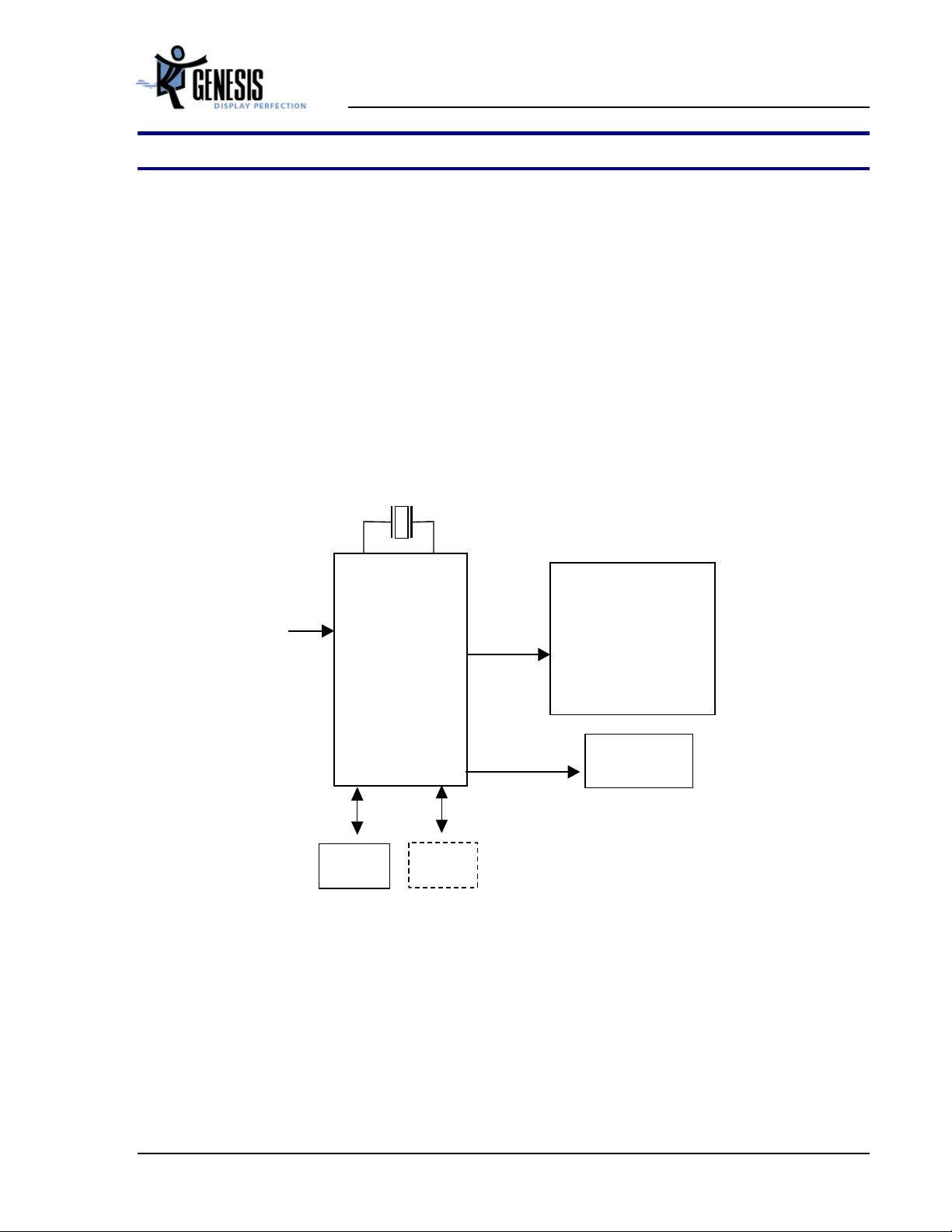
Figure 1 below shows a typical dual interface LCD monitor system based on the gm2121. Designs based
on the gm2121 have reduced system cost, simplified hardware and firmware design and increased
reliability because only a minimal number of components are required in the system.
Analog
RGB
gm2121
Direct
Connect to
LVDS IF
Panels
LCD Module
Back-light
NVRAM
Figure 1. gm2121 System Design Example
EEPROM
(o
tional)
C2121-DAT-01F 8 December 2002
http://www.genesis-microchip.com
Page 9

1.2 gm2121 Features
gm2121 Preliminary Data Sheet
FEATURES
• Zoom (from VGA) and shrink (from UXGA) scaling
• Integrated 8-bit triple-channel ADC / PLL
• Embedded microcontroller with parallel ROM interface
• On-chip versatile OSD engine
• All system clocks synthesized from a single external crystal
• Programmable gamma correction (CLUT)
• RealColor controls provide sRGB compliance
• PWM back light intensity control
• 5-Volt tolerant inputs
• Low EMI and power saving features
High-Quality Advanced Scaling
• Fully programmable zoom ratios
• High-quality shrink capability from UXGA resolution
• Real Recovery function provides full color recovery image
for refresh rates higher than those supported by the LCD
panel
Analog RGB Input Port
• Supports up to 162MHz (SXGA 75Hz / UXGA 60Hz)
• On-chip high-performance PLLs
(only a single reference crystal required)
On-chip Microcontroller
• Requires no external micro-controller
• External parallel ROM interface allows
firmware customization with little additional
cost
• 21 general-purpose inputs/outputs (GPIO's)
and 8 general-purpose outputs (GPO’s)
available for managing system devices
(keypad, back-light, NVRAM, etc)
• Industry-standard firmware embedded onchip, requires no external ROM (configuration
settings stored in NVRAM)
• Low power mode (,0.15W) when no inputs are
active
• Support for DDC2Bi based In-systemProgramming of Flash ROM
Built in Flexible LVDS Transmitter
• Dual four channel 6/8-bit LVDS transmitter
(with high-quality dithering)
• Programmable channel swapping
• Programmable channel polarity
• Support up to SXGA 75Hz output
Highly Integrated System-on-a-Chip
Reduces Component Count for
Highly Cost Effective Solution
Auto-Configuration / Auto-Detection
• Automatic input format detection
• Robust phase and image positioning
RealColor Technology
• Digital brightness and contrast controls
• TV color controls including hue and saturation controls
• Flesh-tone adjustment
• Full color matrix allows end-users to experience the same
colors as viewed on CRTs and other displays (e.g. sRGB
compliance)
On-chip OSD Controller
• On-chip RAM for downloadable menus
• 1, 2 and 4-bit per pixel character cells
• Horizontal and vertical stretch of OSD menus
• Blinking, transparency and blending
Built in Test Pattern Generator
Stand-alone operation requires no
external ROM and no firmware
development for Fast Time to
Market
Firmware compatible Family of
Products:
- gm2110/20 Analog-Interface XGA/SXGA
- gm3110/gm3120 Digital-Interface XGA/SXGA
- gm5110/gm5120 Dual-Interface XGA/SXGA
C2121-DAT-01F 9 December 2002
http://www.genesis-microchip.com
Page 10

gm2121 Preliminary Data Sheet
2 GM2121 Pinout
The gm2121 is available in a 160-pin Plastic Quad Flat Pack (PQFP) package. Figure 2 provides the pin
locations for all signals.
ROM_DATA6
ROM_DATA7
CRVSS
RVDD_3.3
ROM_ADDR0
ROM_ADDR1
ROM_ADDR2
ROM_ADDR3
ROM_ADDR4
ROM_ADDR5
ROM_ADDR6
ROM_ADDR7
ROM_ADDR8
ROM_ADDR9
ROM_ADDR10
ROM_ADDR11
CRVSS
RVDD_3.3
ROM_ADDR12
ROM_ADDR13
ROM_ADDR14
ROM_ADDR15
CVDD_2.5
CRVSS
AVDD_RED_3.3
RED+
RED-
AGND_RED
AVDD_GREEN_3.3
GREEN+
GREEN-
AGND_GREEN
AVDD_BLUE_3.3
BLUE+
BLUE-
AGND_BLUE
AVDD_ADC_3.3
ADC_TEST
AGND_ADC
SGND_ADC
GND1_ADC
ROM_DATA5
ROM_DATA4
ROM_DATA3
ROM_DATA2
ROM_DATA1
ROM_DATA0
ROM_OEn
GPIO22/HCLK
GPIO16/HFSn
GPIO20/HDATA3
GPIO19/HDATA2
GPIO18/HDATA1
GPIO17/HDATA0
RVDD_3.3
CRVSS
GPIO21/IRQn
RESETn
GPIO15/DDC_SCL
GPIO14/DDC_SDA
CVDD_2.5
CRVSS
GPIO8/IRQINn
GPIO0/PWM0
GPIO1/PWM1
GPIO2/PWM2
GPIO3/TIMER1
GPIO4/UART_DI
GPIO5/UART_DO
GPIO6
RVDD_3.3
CRVSS
GPIO7
GPIO9
GPIO11/ROM_WEn
GPIO12/NVRAM_SDA
GPIO13/NVRAM_SCL
GPIO10
STI_TM1
STI_TM2
PPWR
1
160
159
158
157
156
155
154
153
152
151
150
149
148
147
146
145
144
143
142
141
140
139
138
137
136
135
134
133
132
131
130
129
128
2
3
4
5
6
7
8
9
10
11
12
13
14
15
16
17
18
19
20
21
22
23
24
25
26
27
28
29
30
31
32
33
34
35
36
37
38
39
40
414243444546474849505152535455565758596061626364656667686970717273747576777879
gm2121
127
126
125
124
123
122
121
80
120
119
118
117
116
115
114
113
112
111
110
109
108
107
106
105
104
103
102
101
100
99
98
97
96
95
94
93
92
91
90
89
88
87
86
85
84
83
82
81
VDD1_ADC_2.5
GND2_ADC
VDD2_ADC_2.5
VSS_SDDS
VDD_SDDS_3.3
AVSS_SDDS
AVDD_SDDS_3.3
VBUFC
VSS_DDDS
VDD_DDDS_3.3
AVSS_DDDS
AVDD_DDDS_3.3
VSS_DPLL
VDD_DPLL_3.3
AVSS_RPLL
AVDD_RPLL_3.3
XTAL
TCLK
HSYNC
VSYNC
CRVSS
CVDD_2.5
GPO 7
GPO 6
GPO 5
GPO 4
GPO 3
GPO 2
CRVSS
RVDD_3.3
GPO 1
GPO 0
RESERVED
RESERVED
RESERVED
RESERVED
RESERVED
RESERVED
RESERVED
PBIAS
CRVSS
CVDD_2.5
CRVSS
VCO_LV
AVDD_OUT_LV_E_2.5
CLKP_LV_E
CH3P_LV_E
CLKN_LV_E
CH2P_LV_E
CH3N_LV_E
AVSS_OUT_LV_E
CH1P_LV_E
CH2N_LV_E
CH1N_LV_E
AVSS_LV_E
CH0P_LV_E
CH0N_LV_E
AVDD_LV_E_2.5
AVSS_OUT_LV_E
AVDD_OUT_LV_E_2.5
AVSS_OUT_LV_O
CH3P_LV_O
AVDD_OUT_LV_O_2.5
CH3N_LV_O
CLKP_LV_O
CLKN_LV_O
CH2P_LV_O
CH2N_LV_O
CH1P_LV_O
CH1N_LV_O
CH0P_LV_O
CH0N_LV_O
AVSS_OUT_LV_O
AVDD_OUT_LV_O_2.5
AVSS_LV_O
CRVSS
AVDD_LV_O_2.5
CVDD_2.5
RESERVED
Figure 2. gm2121 Pin Out Diagram
C2121-DAT-01F 10 December 2002
http://www.genesis-microchip.com
Page 11
gm2121 Preliminary Data Sheet
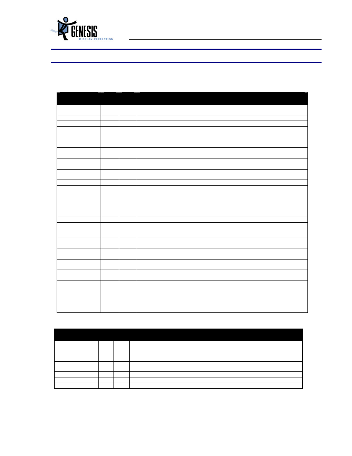
3 GM2121Pin List
I/O Legend: A = Analog, I = Input, O = Output, P = Power, G= Ground
Table 1. Analog Input Port
Pin Name No. I/O Description
AVDD_RED_3.3 136 AP Analog power (3.3V) for the red channel. Must be bypassed with decoupling capacitor to
AGND_RED pin on system board (as close as possible to the pin).
RED+ 135 AI Positive analog input for Red channel.
RED- 134 AI Negative analog input for Red channel.
AGND_RED 133 AG Analog ground for the red channel.
Must be directly connected to the system ground plane.
AVDD_GREEN_3.3 132 AP Analog power (3.3V) for the green channel. Must be bypassed with decoupling capacitor to
AGND_GREEN pin on system board (as close as possible to the pin).
GREEN+ 131 AI Positive analog input for Green channel.
GREEN- 130 AI Negative analog input for Green channel.
AGND_GREEN 129 AG Analog ground for the green channel.
Must be directly connected to the system ground plane.
AVDD_BLUE_3.3 128 AP Analog power (3.3V) for the blue channel. Must be bypassed with decoupling capacitor to
AGND_BLUE pin on system board (as close as possible to the pin).
BLUE+ 127 AI Positive analog input for Blue channel.
BLUE- 126 AI Negative analog input for Blue channel.
AGND_BLUE 125 AG Analog ground for the blue channel.
Must be directly connected to the system ground plane.
AVDD_ADC_3.3 124 AP Analog power (3.3V) for ADC analog blocks that are shared by all three channels. Includes
band gap reference, master biasing and full-scale adjust. Must be bypassed with
decoupling capacitor to AGND_ADC pin on system board (as close as possible to the pin).
ADC_TEST 123 AO Analog test output for ADC Do not connect.
AGND_ADC 122 AG Analog ground for ADC analog blocks that are shared by all three channels. Includes band
gap reference, master biasing and full-scale adjust.
Must be directly connected to system ground plane.
SGND_ADC 121 AG Dedicated pad for substrate guard ring that protects the ADC reference system.
Must be directly connected to the system ground plane.
GND1_ADC 120 G Digital GND for ADC clocking circuit.
Must be directly connected to the system ground plane
VDD1_ADC_2.5 119 P Digital power (2.5V) for ADC encoding logic. Must be bypassed with decoupling capacitor to
GND1_ADC pin on system board (as close as possible to the pin).
GND2_ADC 118 G Digital GND for ADC clocking circuit.
Must be directly connected to the system ground plane.
VDD2_ADC_2.5 117 P Digital power (2.5V) for ADC encoding logic. Must be bypassed with decoupling capacitor to
GND2_ADC pin on system board (as close as possible to the pin).
HSYNC 101 I ADC input horizontal sync input.
[Input, Schmitt trigger (400mV typical hysteresis), 5V-tolerant]
VSYNC 100 I ADC input vertical sync input.
[Input, Schmitt trigger (400mV typical hysteresis), 5V-tolerant]
Table 2. RCLK PLL Pins
Pin Name No I/O Description
AVDD_RPLL_3.3 104 AP Analog power for the Reference DDS PLL. Connect to 3.3V supply. Must be bypassed with a
AVSS_RPLL 105 AG Analog ground for the Reference DDS PLL.
TCLK 102 AI Reference clock (TCLK) from the 20.0MHz crystal oscillator (see Figure 4), or from single-
XTAL 103 AO Crystal oscillator output.
VDD_DPLL_3.3 106 P Digital power for FCLK and RCLK PLLs. Connect to 3.3V supply.
VSS_DPLL 107 G Digital ground for FCLK and RCLK PLLs.
C2121-DAT-01F 11 December 2002
0.1uF capacitor to pin AVSS_RPLL (as close to the pin as possible).
Must be directly connected to the system ground plane.
ended CMOS/TTL clock oscillator (see Figure 7). This is a 5V-tolerant input. See Table 12.
http://www.genesis-microchip.com
Page 12
gm2121 Preliminary Data Sheet
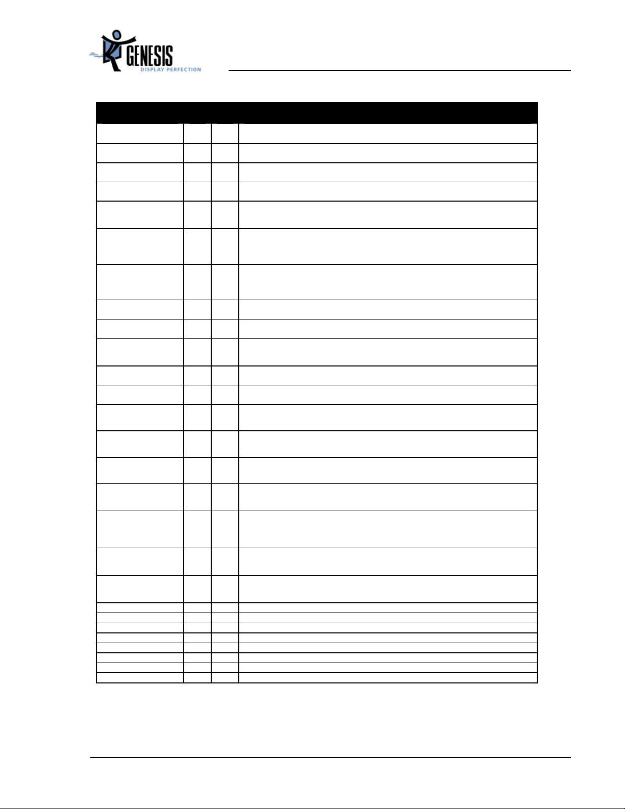
Table 3. System Interface and GPIO Signals
Pin Name No I/O Description
RESETn 17 I
GPIO0/PWM0 23 IO General-purpose input/output signal or PWM0. Open drain option via register setting.
GPIO1/PWM1 24 IO General-purpose input/output signal or PWM1. Open drain option via register setting.
GPIO2/PWM2 25 IO General-purpose input/output signal or PWM2. Open drain option via register setting.
GPIO3/TIMER1 26 IO General-purpose input/output signal. Open drain option via register setting. This pin is also
GPIO4/UART_DI 27 IO General-purpose input/output signal. Open drain option via register setting. This pin is also
GPIO5/UART_DO 28 IO General-purpose input/output signal. Open drain option via register setting. This pin is also
GPIO6 29 IO General-purpose input/output signal.
GPIO7 32 IO General-purpose input/output signal.
GPIO8/IRQINn 22 IO General-purpose input/output signal. This is also active-low interrupt input to OCM and is
GPIO9 33 IO General-purpose input/output signal. Open drain option via register setting.
GPIO10 34 IO General-purpose input/output signal. Open drain option via register setting.
GPIO11/ROM_WEn 35 IO General-purpose input/output signal, or ROM write enable if a programmable FLASH
GPIO12/NVRAM_SDA
GPIO13/NVRAM_SCL
GPIO14/DDC_SCL
GPIO15/DDC_SDA
GPIO16/HFSn 9 IO General-purpose input/output signal when host port is disabled, or data signal for 2-wire
GPIO17/HDATA0
GPIO18/HDATA1
GPIO19/HDATA2
GPIO20/HDATA3
GPIO21/IRQn 16 IO General-purpose input/output signal when host port is disabled, or active-low and open-
GPIO22/HCLK 8 IO General-purpose input/output signal when host port is disabled, or clock for 2-wire serial
GPO 0 88 O General-purpose output signal.
GPO 1 89 O General-purpose output signal
GPO 2 92 O General-purpose output signal
GPO 3 93 O General-purpose output signal
GPO 4 94 O General-purpose output signal
GPO 5 95 O General-purpose output signal
GPO 6 96 O General-purpose output signal
GPO 7 97 O General-purpose output signal
36
37
18
19
13
12
11
10
Active-low hardware reset signal. The reset signal must be held low for at least 1µS.
[Input, Schmitt trigger (400mV typical hysteresis), 5V-tolerant]
[Bi-directional, Schmitt trigger (400mV typical hysteresis), 5V-tolerant]
[Bi-directional, Schmitt trigger (400mV typical hysteresis), 5V-tolerant]
[Bi-directional, Schmitt trigger (400mV typical hysteresis), 5V-tolerant]
connected to Timer 1 clock input of the OCM.
[Bi-directional, Schmitt trigger (400mV typical hysteresis), 5V-tolerant]
connected to the OCM UART data input signal by programming an OCM register. Add
10K Pull-up to VDD_3.3.
[Bi-directional, Schmitt trigger (400mV typical hysteresis), 5V-tolerant]
connected to the OCM UART data output signal by programming an OCM register. Add
10K Pull-up to VDD_3.3.
[Bi-directional, Schmitt trigger (400mV typical hysteresis), 5V-tolerant]
[Bi-directional, Schmitt trigger (400mV typical hysteresis), 5V-tolerant]
[Bi-directional, Schmitt trigger (400mV typical hysteresis), 5V-tolerant]
directly wired to OCM int_0n.
[Bi-directional, Schmitt trigger (400mV typical hysteresis), 5V-tolerant]
[Bi-directional, Schmitt trigger (400mV typical hysteresis), 5V-tolerant]
[Bi-directional, Schmitt trigger (400mV typical hysteresis), 5V-tolerant]
device is used. Open drain option via register setting.
[Bi-directional Input, Schmitt trigger (400mV typical hysteresis), 5V-tolerant]
IO
General-purpose input/output signals, or 2-wire master serial interface to NVRAM in
standalone mode. Open drain option via register setting.
IO
[Bi-directional Input, Schmitt trigger (400mV typical hysteresis), 5V-tolerant]
IO General-purpose input/output signals, or 2-wire master serial interface to NVRAM in
standalone mode. Open drain option via register setting.
[Bi-directional Input, Schmitt trigger (400mV typical hysteresis), 5V-tolerant]
serial host interface.
[Bi-directional, Schmitt trigger (400mV typical hysteresis), slew rate limited, 5V tolerant]
IO
General-purpose input/output signals.
IO
[Bi-directional, Schmitt trigger (400mV typical hysteresis), 5V-tolerant]
IO
IO
drain interrupt output pin.
[Bi-directional, 5V-tolerant]
host interface.
[Bi-directional, Schmitt trigger (400mV typical hysteresis), 5V-tolerant]
C2121-DAT-01F 12 December 2002
http://www.genesis-microchip.com
Page 13
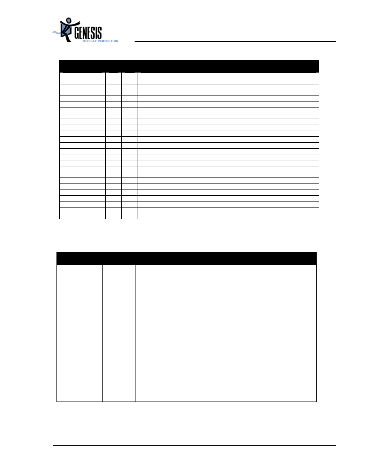
Table 4. Display Output Port
Pin Name No I/O Description
PBIAS 41 O Panel Bias Control (back light enable)
[Tri-state output, Programmable Drive]
PPWR 40 O Panel Power Control
[Tri-state output, Programmable Drive]
CH3P_LV_E 48 O Even LVDS Channel 3 positive
CH3N_LV_E 49 O Even LVDS Channel 3 negative
CLKP_LV_E 50 O Even LVDS Clock positive
CLKN_LV_E 51 O Even LVDS Clock negative
CH2P_LV_E 52 O Even LVDS Channel 2 positive
CH2N_LV_E 53 O Even LVDS Channel 2 negative
CH1P_LV_E 54 O Even LVDS Channel 1 positive
CH1N_LV_E 55 O Even LVDS Channel 1 negative
CH0P_LV_E 56 O Even LVDS Channel 0 positive
CH0N_LV_E 57 O Even LVDS Channel 0 negative
CH3P_LV_O 64 O Odd LVDS Channel 3 positive
CH3N_LV_O 65 O Odd LVDS channel 3 negative
CLKP_LV_O 66 O Odd LVDS Clock positive
CLKN_LV_O 67 O Odd LVDS Clock negative
CH2P_LV_O 68 O Odd LVDS Channel 2 positive
CH2N_LV_O 69 O Odd LVDS channel 2 negative
CH1P_LV_O 70 O Odd LVDS Channel 1 positive
CH1N_LV_O 71 O Odd LVDS channel 1 negative
CH0P_LV_O 72 O Odd LVDS Channel 0 positive
CH0N_LV_O 73 O Odd LVDS channel 0 negative
gm2121 Preliminary Data Sheet
Table 5. Parallel ROM Interface Port
Pin Name No I/O Description
ROM_ADDR15
ROM_ADDR14
ROM_ADDR13
ROM_ADDR12
ROM_ADDR11
ROM_ADDR10
ROM_ADDR9
ROM_ADDR8
ROM_ADDR7
ROM_ADDR6
ROM_ADDR5
ROM_ADDR4
ROM_ADDR3
ROM_ADDR2
ROM_ADDR1
ROM_ADDR0
ROM_DATA7
ROM_DATA6
ROM_DATA5
ROM_DATA4
ROM_DATA3
ROM_DATA2
ROM_DATA1
ROM_DATA0
ROM_OEn 7 O External PROM data Output Enable
139
140
141
142
145
146
147
148
149
150
151
152
153
154
155
156
159
160
1
2
3
4
5
6
IO
ROM address output. These pins also serve as 5V-tolerant bootstrap inputs on power up.
IO
IO
IO
IO
IO
IO
IO
IO
IO
IO
IO
IO
IO
IO
IO
I
5V-tolerant external PROM data input
I
I
I
I
I
I
I
C2121-DAT-01F 13 December 2002
http://www.genesis-microchip.com
Page 14
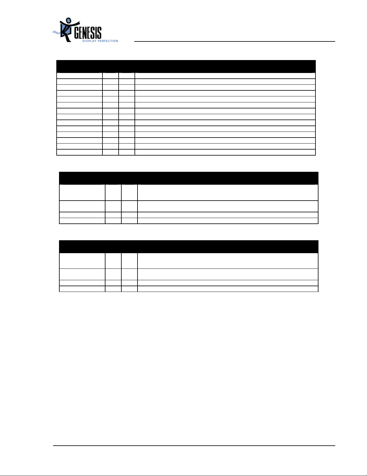
Table 6. Reserved Pins
Pin Name No I/O Description
Reserved 80 O For test purposes only. Do not connect
Reserved 81 O For test purposes only. Do not connect
Reserved 82 O For test purposes only. Do not connect
Reserved 83 O For test purposes only. Do not connect
Reserved 84 O For test purposes only. Do not connect
Reserved 85 O For test purposes only. Do not connect
Reserved 86 O For test purposes only. Do not connect
Reserved 87 O For test purposes only. Do not connect
VBUFC 112 O For test purposes only. Do not connect
VCO_LV 45 O For test purposes only. Do not connect
STI_TM1 38 I For test purposes only. MUST be tied to GND
STI_TM2 39 I For test purposes only. MUST be tied to GND
Table 7. Power and Ground Pins for ADC Sampling Clock DDS
Pin Name No I/O Description
AVDD_SDDS_3.3 113 AP Analog power for the Source DDS. Connect to 3.3V supply.
Must be bypassed with a 0.1uF capacitor to AVSS_SDDS pin
(as close to the pin as possible).
AVSS_SDDS 114 AG Analog ground for the Source DDS.
Must be directly connected to the system ground.
VDD_SDDS_3.3 115 P Digital power for the Source DDS. Connect to 3.3V supply.
VSS_SDDS 116 G Digital ground for the Source DDS.
gm2121 Preliminary Data Sheet
Table 8. Power and Ground Pins for Display Clock DDS
Pin Name No I/O Description
AVDD_DDDS_3.3 108 AP Analog power for Destination DDS. Connect to 3.3V supply.
AVSS_DDDS 109 AG Analog ground for Destination DDS.
VDD_DDDS_3.3 110 P Digital power for the Destination DDS. Connect to 3.3V supply.
VSS_DDDS 111 G Digital ground for the Destination DDS.
Must be bypassed with a 0.1uF capacitor to AVSS_DDDS pin
(as close to the pin as possible).
Must be directly connected to the system ground plane.
C2121-DAT-01F 14 December 2002
http://www.genesis-microchip.com
Page 15
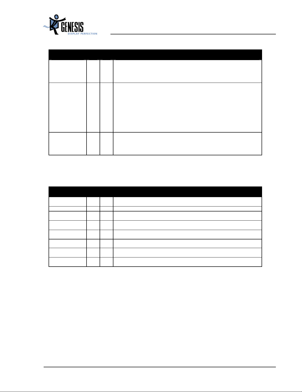
gm2121 Preliminary Data Sheet
Table 9. I/O Power and Ground Pins
Pin Name No I/O Description
RVDD_3.3 14
143
157
CRVSS 15
137
144
158
CVDD_2.5 20
138
Note, “AP” indicates a power supply that is analog in nature and does not have large switching currents.
These should be isolated from other digital supplies that do have large switching currents.
30
90
21
31
42
44
78
91
99
43
79
98
P
Connect to 3.3V digital supply.
P
Must be bypassed with a 0.1uF capacitor to CRVSS (as close to the pin as possible).
P
P
P
G
Connect to digital ground.
G
G
G
G
G
G
G
G
G
G
P
Connect to 2.5V digital supply.
P
Must be bypassed with a 0.1uF capacitor to CRVSS (as close to the pin as possible).
P
P
P
Table 10.
Power and Ground Pins for LVDS Transmitter
Pin Name No I/O Description
AVDD_OUT_LV_E_
2.5
AVDD_LV_E_2.5 61 AP Analog power for on-chip LVDS transmitter. Connect to 2.5V supply
AVSS_OUT_LV_E 47
AVSS_LV_E 60 G Analog ground for on-chip LVDS transmitter.
AVDD_OUT_LV_O_
2.5
AVDD_LV_O_2.5 77 AP Analog power for on-chip LVDS transmitter. Connect to 2.5V supply.
AVSS_OUT_LV_O 62
AVSS_LV_O 76 G Analog ground for on-chip LVDS transmitter.
46
AP Analog power for on-chip LVDS output buffer. Connect to 2.5V supply.
59
58
63
74
75
G Analog ground for on-chip LVDS output buffer.
Must be directly connected to the system ground plane
Must be directly connected to the system ground plane
AP Analog power for on-chip LVDS output buffer. Connect to 2.5V supply.
G Analog ground for on-chip LVDS output buffer.
Must be directly connected to the system ground plane.
Must be directly connected to the system ground plane.
C2121-DAT-01F 15 December 2002
http://www.genesis-microchip.com
Page 16
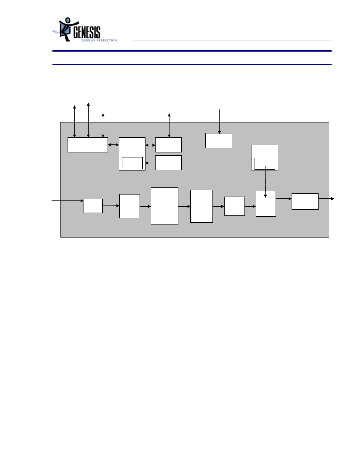
gm2121 Preliminary Data Sheet
4 Functional Description
A functional block diagram is illustrated below. Each of the functional units shown is described in the
following sections.
NVRAM
Serial I/F
Serial Host I/F
GPIO
Parallel
ROM IF
Crystal
Reference
Host
Interface
8051-style
Micro-
controller
MCU
RAM
External
ROM I/F
Internal
ROM
Clock
Generation
OSD
Controller
OSD
RAMs
Analog
RGB
Triple
ADC
Image
Capture /
Measure-
ment
Figure 3. gm2121 Functional Block Diagram
Brightness /
Contrast /
Hue / Sat /
RealColor /
Moire
Zoom /
Shrink /
Filter
Gamma
Control
Output
Data
Path
Dual LVDS
Transmitter
Panel Data
and Control
4.1 Clock Generation
The gm2121 features two clock inputs. All additional clocks are internal clocks derived from one or more
of these:
1. Crystal Input Clock (TCLK and XTAL). This is the input pair to an internal crystal oscillator and
corresponding logic. A 20.0 MHz crystal is recommended. Other crystal frequencies may be used, but
require custom programming. This is illustrated in Figure 4 below. Alternatively, a single-ended
TTL/CMOS clock oscillator can be driven into the TCLK pin (leave XTAL as N/C in this case). This
is illustrated in Figure 7 below. This option is selected by connecting a 10KΩ pull-up to
ROM_ADDR13 (refer to Table 17). See also Table 12.
2. Host Interface Transfer Clock (HCLK)
The gm2121 TCLK oscillator circuitry is a custom designed circuit to support the use of an external
oscillator or a crystal resonator to generate a reference frequency source for the gm2121 device.
C2121-DAT-01F 16 December 2002
http://www.genesis-microchip.com
Page 17
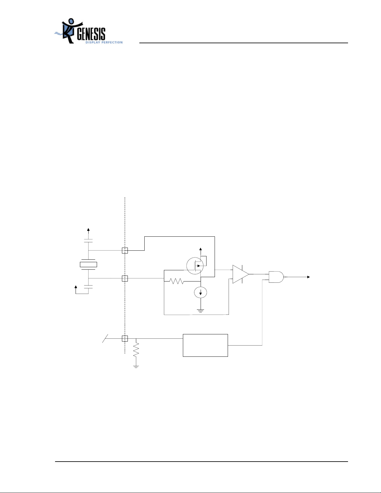
gm2121 Preliminary Data Sheet
4.1.1 Using the Internal Oscillator with External Crystal
The first option for providing a clock reference is to use the internal oscillator with an external crystal.
The oscillator circuit is designed to provide a very low jitter and very low harmonic clock to the internal
circuitry of the gm2121. An Automatic Gain Control (AGC) is used to insure startup and operation over a
wide range of conditions. The oscillator circuit also minimizes the overdrive of the crystal, which reduces
the aging of the crystal.
When the gm2121 is in reset, the state of the ROM_ADDR13 pin is sampled. If the pin is left
unconnected (internal pull-down) then internal oscillator is enabled. In this mode a crystal resonator is
connected between TCLK and the XTAL with the appropriately sized loading capacitors C
size of C
and CL2 are determined from the crystal manufacturer’s specification and by compensating for
L1
and CL2. The
L1
the parasitic capacitance of the gm2121 device and the printed circuit board traces. The loading capacitors
are terminated to the analog VDD power supply. This connection increases the power supply rejection
ratio when compared to terminating the loading capacitors to ground.
gm2121
Internal Pull Down
Resistor
~ 60K
100 K
Vdd
180 uA
Reset State Logic
Internal Oscillator Enable
OSC_OUT
TCLK Distribution
Vdda
Vdda
CL1
CL2
N/C
ROM_ADDR13
102
TCLK
103
XTAL
141
Figure 4. Using the Internal Oscillator with External Crystal
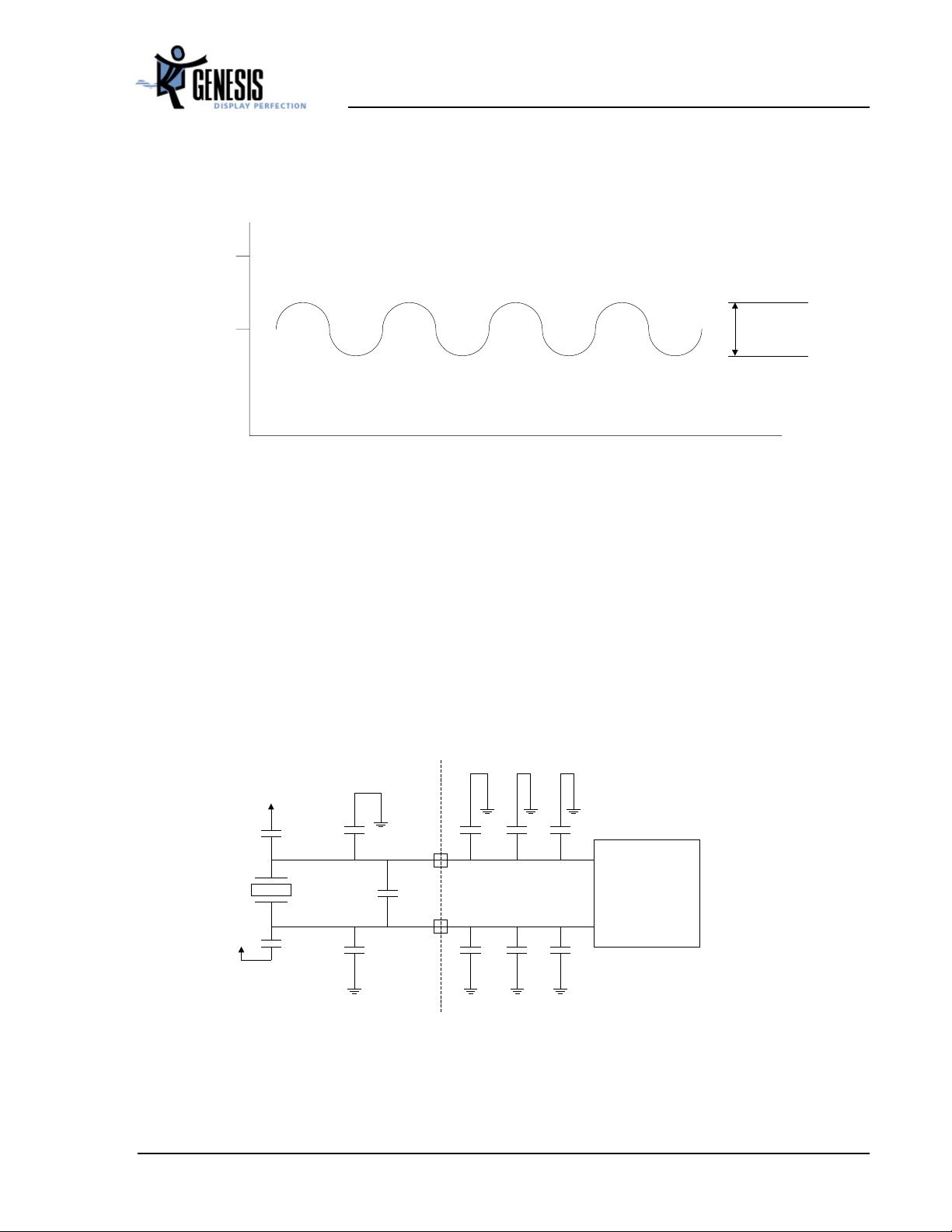
The TCLK oscillator uses a Pierce Oscillator circuit. The output of the oscillator circuit, measured at the
TCLK pin, is an approximate sine wave with a bias of about 2 volts above ground (see Figure 5). The
peak-to-peak voltage of the output can range from 250 mV to 1000 mV depending on the specific
characteristics of the crystal and variation in the oscillator characteristics. The output of the oscillator is
connected to a comparator that converts the sine wave to a square wave. The comparator requires a
C2121-DAT-01F 17 December 2002
http://www.genesis-microchip.com
Page 18
A
gm2121 Preliminary Data Sheet
minimum signal level of about 50-mV peak to peak to function correctly. The output of the comparator is
buffered and then distributed to the gm2121 circuits.
3.3 Volts
250 mV peak to peak
~ 2 Volts
to
1000 mV peak to peak
time
Figure 5. Internal Oscillator Output
One of the design parameters that must be given some consideration is the value of the loading capacitors
used with the crystal as shown in Figure 6. The loading capacitance (C
combination of C
capacitance C
approximately 9 pF. C
PCB board capacitance (C
protection capacitance (C
C
pad
+ C
. The correct value of Cex must be calculated based on the values of the load capacitances.
ESD
and CL2 and is calculated by C
L1
is the effective capacitance between the XTAL and TCLK pins. For the gm2121 this is
shunt
and CL2 are a parallel combination of the external loading capacitors (Cex), the
L1
), the pin capacitance (C
pcb
). The capacitances are symmetrical so that CL1 = CL2 = Cex + C
esd
= ((CL1 * CL2) / (CL1 + CL2)) + C
load
), the pad capacitance (C
pin
) on the crystal is the
load
shunt
), and the ESD
pad
. The shunt
+ C
PCB
pin
+
Approximate values are provided in Figure 6.
CL1 = Cex1 + Cpcb + Cpin + Cpad + Cesd
Vdda
Cex1
Cpcb
Cshunt
102
TCLK
103
Cpin Cpad Ce sd
Internal Oscillator
gm2121
Vdda
Cex2
CL2 = Cex1 + Cpcb + Cpin + Cpad + Cesd
Cpcb
XTAL
Cpin Cpad Cesd
pproximate values:
C
~ 2 pF to 10 pF (layout dependent)
PCB
C
~ 1.1 pF
pin
~ 1 pF
C
pad
~ 5.3 pF
C
esd
C
~ 9 pF
shunt
Figure 6. Sources of Parasitic Capacitance
C2121-DAT-01F 18 December 2002
http://www.genesis-microchip.com
Page 19
gm2121 Preliminary Data Sheet
Some attention must be given to the details of the oscillator circuit when used with a crystal resonator.
The PCB traces should be as short as possible. The value of C
that is specified by the manufacturer
load
should not be exceeded because of potential start up problems with the oscillator. Additionally, the crystal
should be a parallel resonate-cut and the value of the equivalent series resistance must be less then 90
Ohms.
4.1.2 Using an External Clock Oscillator
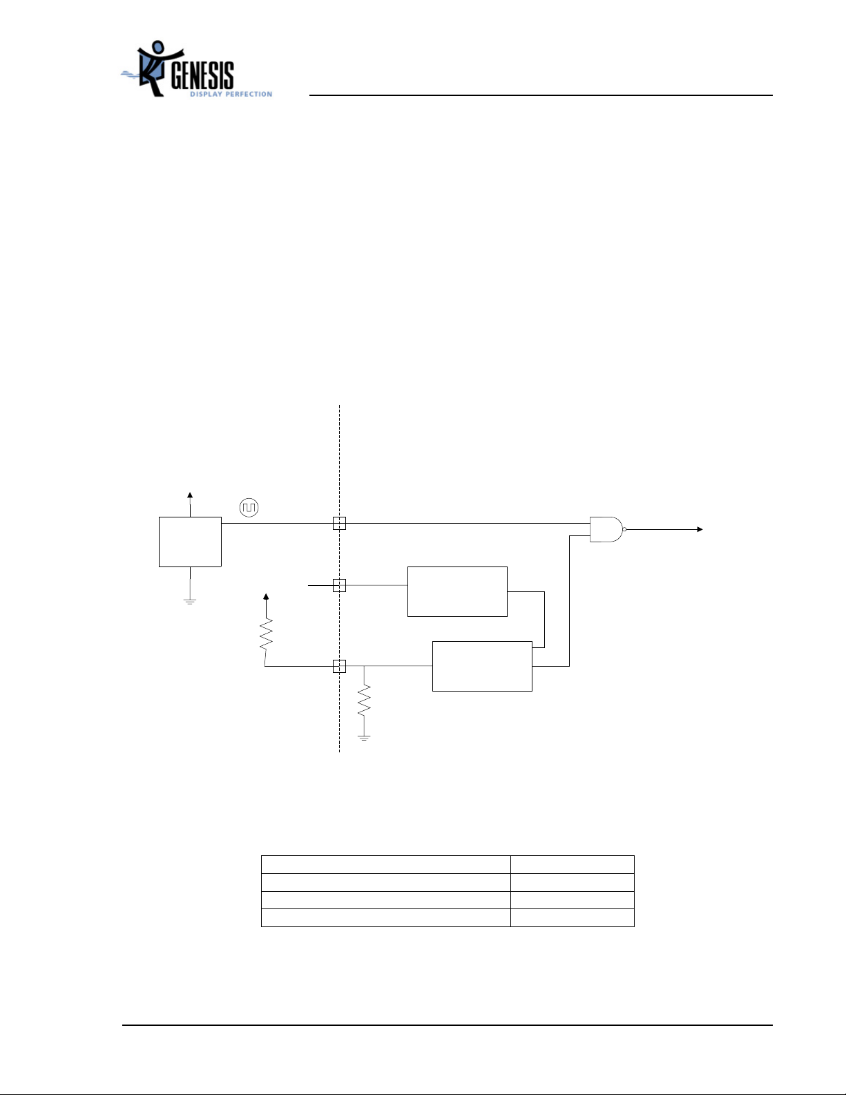
Another option for providing the reference clock is to use a single-ended external clock oscillator. When
the gm2121 is in reset, the state of the ROM_ADDR13 is sampled. If ROM_ADDR13 is pulled high by
connecting to VDD through a pull-up resistor (10KΩ recommended, 15KΩ maximum) then external
oscillator mode is enabled. In this mode the internal oscillator circuit is disabled and the external
oscillator signal that is connected to the TCLK pin is routed to an internal clock buffer. This is illustrated
in Figure 7.
Vdd
Vdd
Oscillator
GND
14 to 24 MHz
Vdd
10 K
102
TCLK
103
XTAL
ROM_ADDR13
141
gm2121
Internal Pull Down
Resistor
~ 60 K
Internal
Oscillator
Reset State Logic
Disable
External Oscillator Enable
OSC_OUT
TCLK Distribution
Figure 7. Using an External Single-ended Clock Oscillator
Table 11. TCLK Specification
Frequency 14 to 24 MHz
Jitter Tolerance 250 ps
Rise Time (10% to 90%) 5 ns
Maximum Duty Cycle 40-60
C2121-DAT-01F 19 December 2002
http://www.genesis-microchip.com
Page 20
gm2121 Preliminary Data Sheet
4.1.3 Clock Synthesis
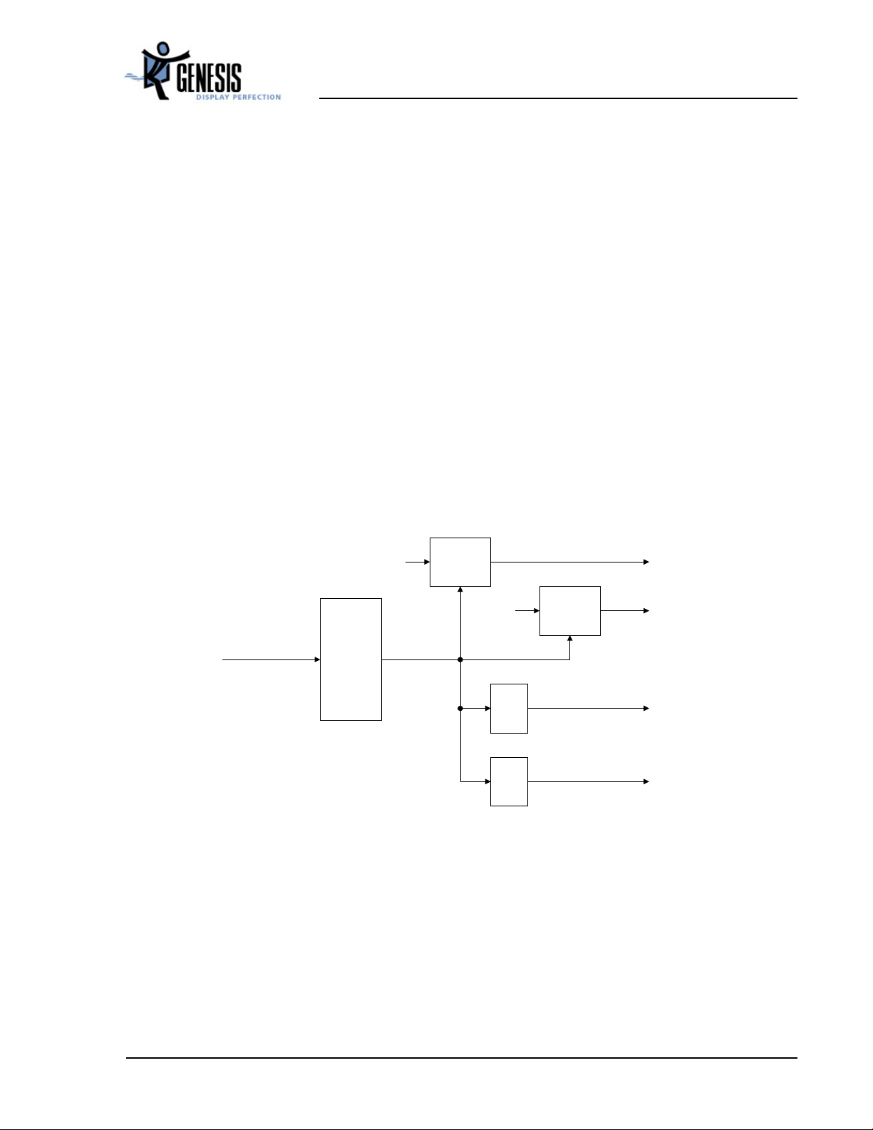
The gm2121 synthesizes all additional clocks internally as illustrated in Figure 8 below. The synthesized
clocks are as follows:
1. Main Timing Clock (TCLK) is the output of the chip internal crystal oscillator. TCLK is derived from
the TCLK/XTAL pad input.
2. Reference Clock (RCLK) synthesized by RCLK PLL (RPLL) using TCLK as the reference.
3. Input Source Clock (SCLK) synthesized by Source DDS (SDDS) PLL using input HSYNC as the
reference. The SDDS internal digital logic is driven by RCLK.
4. Display Clock (DCLK) synthesized by Destination DDS (DDDS) PLL using IP_CLK as the
reference. The DDDS internal digital logic is driven by RCLK.
5. Half Reference Clock (RCLK/2) is the RCLK (see 2, above) divided by 2. Used as OCM_CLK
domain driver.
6. Quarter Reference Clock (RCLK/4) is the RCLK (see 2, above) divided by 4. Used as alternative
clock (faster than TCLK) to drive IFM.
7. ADC Output Clock (SENSE_ACLK) is a delay-adjusted ADC sampling clock, ACLK. ACLK is
derived from SCLK.
TCLK
RCLK
PLL
HSYNC
SDDS
IP_CLK
DDDS
/2
/4
SCLK
DCLK
RCLK/2
RCLK/4
Figure 8. Internally Synthesized Clocks
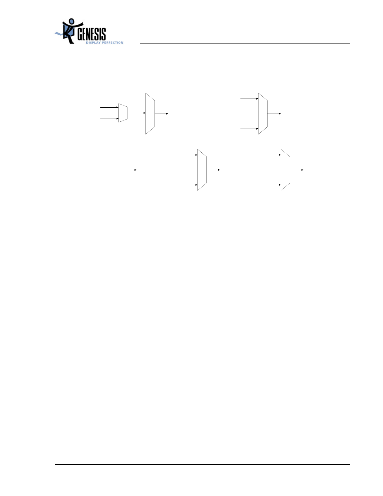
The on-chip clock domains are selected from the synthesized clocks as shown in Figure 9 below. These
include:
1. Input Domain Clock (IP_CLK). Max = 165MHz
2. Host Interface and On-Chip Microcontroller Clock (OCM_CLK). Max = 100MHz
3. Filter and Display Pixel Clock (DP_CLK). Max = 135MHz
4. Source Timing Measurement Domain Clock (IFM_CLK). Max = 50MHz
C2121-DAT-01F 20 December 2002
http://www.genesis-microchip.com
Page 21
gm2121 Preliminary Data Sheet
5. ADC Domain Clock (ACLK). Max = 165MHz.
The clock selection for each domain as shown in the figure below is controlled using the
CLOCK_CONFIG registers (index 0x03 and 0x04).
DCLK
SCLK
SENSE_ACLK
IP_CLK
DP_CLK
IP_CLK
SCLK
RCLK/2
ACLK OCM_CLK
TCLK
RCLK/4
IFM_CLK
TCLK
Figure 9. On-chip Clock Domains
4.2 Chip Initialization
4.2.1 Hardware Reset
Hardware Reset is performed by holding the RESETn pin low for a minimum of 1µs. A TCLK input (see
Clock Options above) must be applied during and after the reset. When the reset period is complete and
RESETn is de-asserted, the power-up sequence is as follows:
1. Reset all registers of all types to their default state (this is 00h unless otherwise specified in the
gm2121 Register Listing).
2. Force each clock domain into reset. Reset will remain asserted for 64 local clock domain cycles
following the de-assertion of RESETn.
3. Operate the OCM_CLK domain at the TCLK frequency.
4. Preset the RCLK PLL to output ~200MHz clock (assumes 20.0MHz TCLK crystal frequency).
5. Wait for RCLK PLL to Lock. Then, switch the OCM_CLK domain to operate from the bootstrap
selected clock.
6. If a pull-up resistor is installed on ROM_ADDR9 pin (see Table 17), then the OCM becomes active
as soon as OCM_CLK is stable. Otherwise, the OCM remains in reset until OCM_CONTROL
register (0x22) bit 1 is enabled.
C2121-DAT-01F 21 December 2002
http://www.genesis-microchip.com
Page 22
gm2121 Preliminary Data Sheet
4.2.2 Correct Power Sequencing
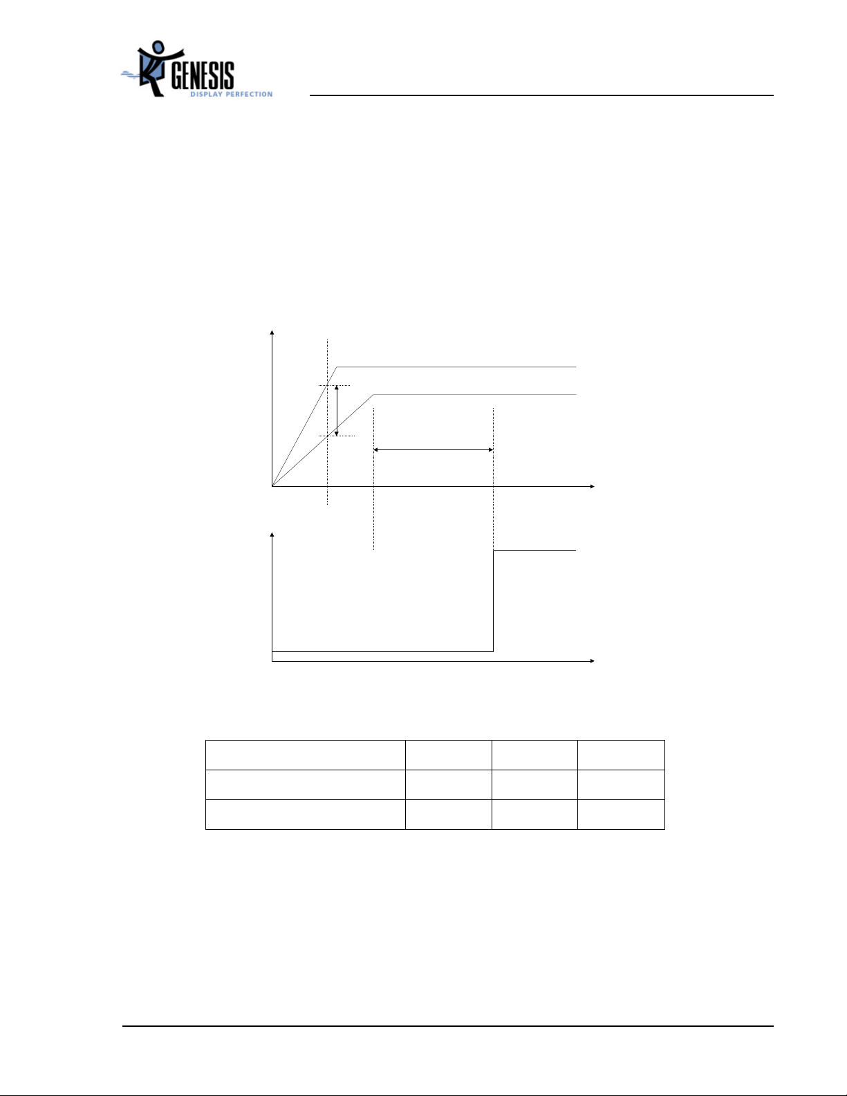
The system designer must ensure that the 2.5V CVDD and 3.3V RVDD power supply rails power up in
the correct sequence. That is, at any time during the power-up sequence the actual voltage of the 3.3V
RVDD power supply should always be equal to or higher than the actual voltage of the 2.5V CVDD
power supply. In mathematical terms, V
RVDD
>= V
at all times. This is illustrated in Figure 10.
CVDD
In addition, the system designer must ensure that the 2.5V core VDD supply must be active for at least
1ms before the rising edge of the chip RESETn signal during the chip power-up sequence. The rising
edge of RESETn signal is used to latch the bootstrap configurations, so its correct timing relationship to
the core VDD is critical for correct chip operation.
Voltage
RVDD (3.3V)
CVDD (2.5V)
V
RVDD-CVDD
(t)
T
CVDD->RESETn
Time
t
Voltage
0V
Time
RESETn
Figure 10. Correct Power Sequencing
Parameter Min Typ Max
V
RVDD-CVDD
T
CVDD->RESETn
(for all t>0) 0V
1ms
4.3 Analog to Digital Converter
The gm2121 chip has three ADC’s (analog-to-digital converters), one for each color (red, green, and
blue).
C2121-DAT-01F 22 December 2002
http://www.genesis-microchip.com
Page 23
gm2121 Preliminary Data Sheet
4.3.1 ADC Pin Connection
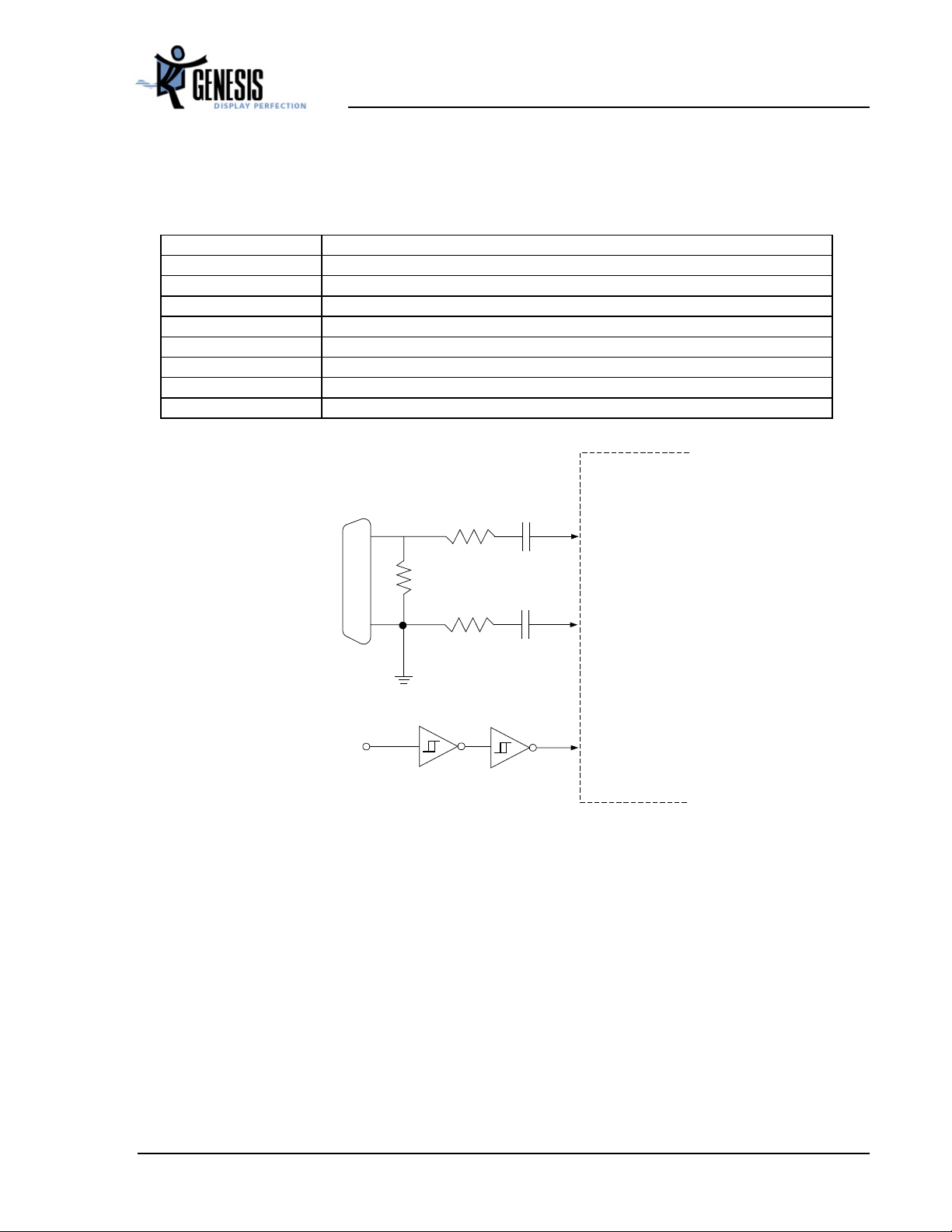
The analog RGB signals are connected to the gm2121 as described below:
Table 12. Pin Connection for RGB Input with HSYNC/VSYNC
Pin Name ADC Signal Name
Red+ Red
Red- Terminate as illustrated in Figure 11
Green+ Green
Green- Terminate as illustrated in Figure 11
Blue+ Blue
Blue- Terminate as illustrated in Figure 11
HSYNC Horizontal Sync (Terminate as illustrated in Figure 11)
VSYNC Vertical Sync (Terminate as with HSYNC illustrated in Figure 11)
gm2121
20
Ω
RED
RED +
0.01uF
Ω
RED -
0.01uF
HS
DB15
HSYNC
GND
75
Ω
57.6
Figure 11. Example ADC Signal Terminations
Please note that it is very important to follow the recommended layout guidelines for the circuit shown in
Figure 11. These are described in "gm5115 Layout Guidelines" document number C5115-SLG-01A.
4.3.2 ADC Characteristics
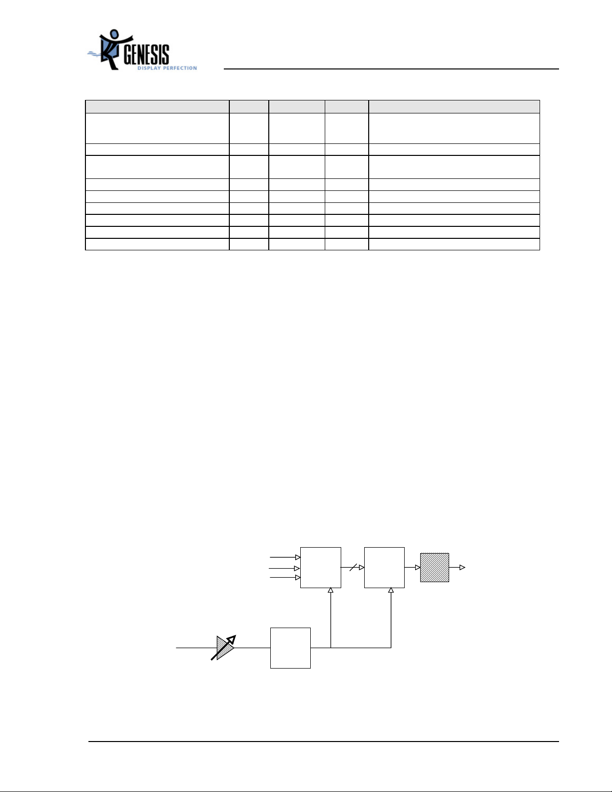
The table below summarizes the characteristics of the ADC:
C2121-DAT-01F 23 December 2002
http://www.genesis-microchip.com
Page 24
gm2121 Preliminary Data Sheet
Table 13. ADC Characteristics
MIN TYP MAX NOTE
Track & Hold Amp Bandwidth 290 MHz Guaranteed by design. Note that the Track &
Hold Amp Bandwidth is programmable. 290
MHz is the maximum setting.
Full Scale Adjust Range at RGB Inputs 0.55 V 0.90 V
Full Scale Adjust Sensitivity +/- 1 LSB Measured at ADC Output.
Independent of full scale RGB input.
Zero Scale Adjust Sensitivity +/- 1 LSB Measured at ADC Output.
Sampling Frequency (Fs) 10 MHz 162.5 MHz
Differential Non-Linearity (DNL) +/-0.5 LSB +/-0.9 LSB Fs = 135 MHz
No Missing Codes Guaranteed by test.
Integral Non-Linearity (INL) +/- 1.5 LSB Fs =135 MHz
Channel to Channel Matching +/- 0.5 LSB
Note that input formats with resolutions or refresh rates higher than that supported by the LCD panel are
supported as recovery modes only. This is called RealRecovery™. For example, it may be necessary to
shrink the image. This may introduce image artifacts. However, the image is clear enough to allow the
user to change the display properties.
The gm2121 ADC has a built in clamp circuit for AC-coupled inputs. By inserting series capacitors
(about 10 nF), the DC offset of an external video source can be removed. The clamp pulse position and
width are programmable.
4.3.3 Clock Recovery Circuit
The SDDS (Source Direct Digital Synthesis) clock recovery circuit generates the clock used to sample
analog RGB data (IP_CLK or source clock). This circuit is locked to HSYNC of the incoming video
signal.
Patented digital clock synthesis technology makes the gm2121 clock circuits resistant to
temperature/voltage drift. Using DDS (Direct Digital Synthesis) technology, the clock recovery circuit
can generate any IP_CLK clock frequency within the range of 10MHz to 165MHz.
Image Phase
Measurement
HSYNC
Phase
HSYNC
(delayed)
R
G
ADC
B
SDDS
24
IPCLK
Window
Capture
Figure 12. gm2121 Clock Recovery
C2121-DAT-01F 24 December 2002
http://www.genesis-microchip.com
Page 25
gm2121 Preliminary Data Sheet
4.3.4 Sampling Phase Adjustment
The programmable ADC sampling phase is adjusted by delaying the HSYNC input to the SDDS. The
accuracy of the sampling phase is checked and the result read from a register. This feature enables
accurate auto-adjustment of the ADC sampling phase.
4.3.5 ADC Capture Window
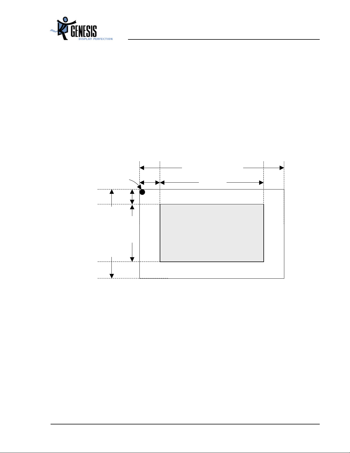
Figure 13 below illustrates the capture window used for the ADC input. In the horizontal direction the
capture window is defined in IP_CLKs (equivalent to a pixel count). In the vertical direction it is defined
in lines.
All the parameters beginning with “Source” are programmed gm2121 registers values. Note that the input
vertical total is solely determined by the input and is not a programmable parameter.
Reference
Point
Source
Hstart
Source Horizontal Total (pixels)
Source Width
Source
Source
Vstart
Height
Capture Window
Input Vertical Total (lines)
Figure 13. ADC Capture Window
The Reference Point marks the leading edge of the first internal HSYNC following the leading edge of an
internal VSYNC. Both the internal HSYNC and the internal VSYNC are derived from external HSYNC
and VSYNC inputs.
Horizontal parameters are defined in terms of single pixel increments relative to the internal horizontal
sync. Vertical parameters are defined in terms of single line increments relative to the internal vertical
sync.
For ADC interlaced inputs, the gm2121 may be programmed to automatically determine the field type
(even or odd) from the VSYNC/HSYNC relative timing. See Input Format Measurement, Section 4.4.
C2121-DAT-01F 25 December 2002
http://www.genesis-microchip.com
Page 26
gm2121 Preliminary Data Sheet
4.4 Test Pattern Generator (TPG)
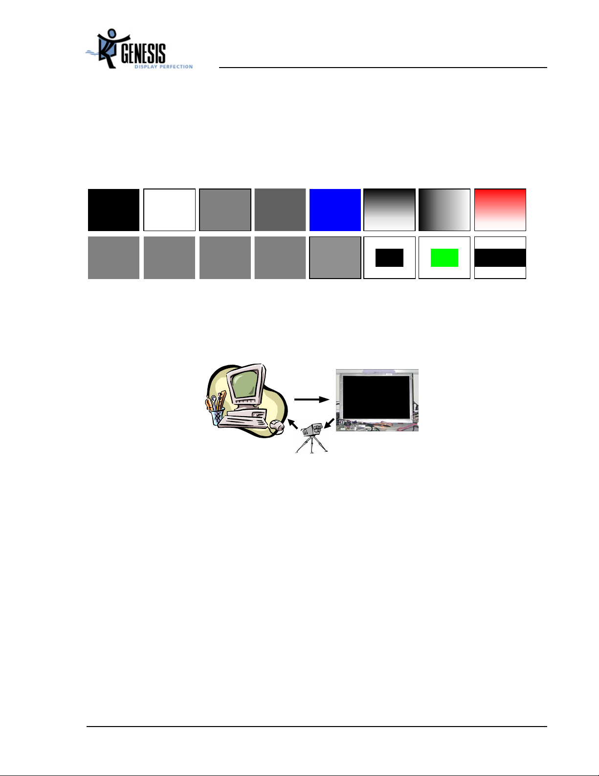
The gm2121 contains hundreds of test patterns, some of which are shown in Figure 14. Once
programmed, the gm2121 test pattern generator can replace a video source (e.g. a PC) during factory
calibration and test. This simplifies the test procedure and eliminates the possibility of image noise being
injected into the system from the source. The foreground and background colors are programmable. In
addition, the gm2121 OSD controller can be used to produce other patterns.
Figure 14. Some of gm2121 built-in test patterns
The DDC2Bi port can be used for factory testing. The factory test station connects to the gm2121 through
the Direct Data Channel (DDC) of the DSUB15 connector. Then, the PC can make gm2121 display test
patterns (see section 4.4). A camera can be used to automate the calibration of the LCD panel.
DDC
Factory Test Station Device-Under-Test
Camera
Figure 15. Factory Calibration and Test Environment
4.5 Input Format Measurement
The gm2121 has an Input Format Measurement block (the IFM) providing the capability of measuring the
horizontal and vertical timing parameters of the input video source. This information may be used to
determine the video format and to detect a change in the input format. It is also capable of detecting the
field type of interlaced formats.
The IFM features a programmable reset, separate from the regular gm2121 soft reset. This reset disables
the IFM, reducing power consumption. The IFM is capable of operating while gm2121 is running in
power down mode.
Horizontal measurements are measured in terms of the selected IFM_CLK (either TCLK or RCLK/4),
while vertical measurements are measured in terms of HSYNC pulses.
C2121-DAT-01F 26 December 2002
http://www.genesis-microchip.com
Page 27
gm2121 Preliminary Data Sheet
For an overview of the internally synthesized clocks, see section 4.1.
4.5.1 HSYNC / VSYNC Delay
The active input region captured by the gm2121 is specified with respect to internal HSYNC and
VSYNC. By default, internal syncs are equivalent to the HSYNC and VSYNC at the input pins and thus
force the captured region to be bounded by external HSYNC and VSYNC timing. However, the gm2121
provides an internal HSYNC and VSYNC delay feature that removes this limitation. This feature is
available for use with the ADC input. By delaying the sync internally, the gm2121 can capture data that
spans across the sync pulse.
It is possible to use HSNYC and VSYNC delay for image positioning. (Alternatively, Source_HSTART
and Source_VSTART in Figure 13 are used for image positioning of analog input.) Taken to an extreme,
the intentional movement of images across apparent HSYNC and VSYNC boundaries creates a horizontal
and/or vertical wrap effect.
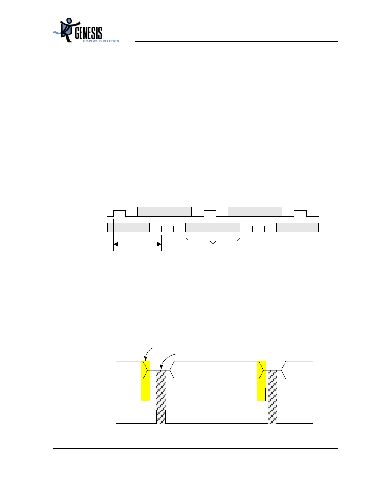
HSYNC is delayed by a programmed number of selected input clocks.
HS(system)
HS(internal)
capture
programmable
delay
active active
capture capture
input block actually
captures across HSYNC
Figure 16. HSYNC Delay
Delayed horizontal sync may be used to solve a potential problem with VSYNC jitter with respect to
HSYNC. VSYNC and HSYNC are generally driven active coincidentally, but with different paths to the
gm2121 (HSYNC is often regenerated from a PLL). As a result, VSYNC may be seen earlier or later.
Because VSYNC is used to reset the line counter and HSYNC is used to increment it, any difference in
the relative position of HSYNC and VSYNC is seen on-screen as vertical jitter. By delaying the HSYNC
a small amount, it can be ensured that VSYNC always resets the line counter prior to it being incremented
by the “first” HSYNC.
active data crosses HS boundary
delayed HS placed safely within blanking
Data
HS (system)
Internal Delayed HS
Figure 17. Active Data Crosses HSYNC Boundary
C2121-DAT-01F 27 December 2002
http://www.genesis-microchip.com
Page 28
gm2121 Preliminary Data Sheet
4.5.2 Horizontal and Vertical Measurement
The IFM is able to measure the horizontal period and active high pulse width of the HSYNC signal, in
terms of the selected clock period (either TCLK or RCLK/4.). Horizontal measurements are performed on
only a single line per frame (or field). The line used is programmable. It is able to measure the vertical
period and VSYNC pulse width in terms of rising edges of HSYNC.
Once enabled, measurement begins on the rising VSYNC and is completed on the following rising
VSYNC. Measurements are made on every field / frame until disabled.
4.5.3 Format Change Detection
The IFM is able to detect changes in the input format relative to the last measurement and then alert both
the system and the on-chip microcontroller. The microcontroller sets a measurement difference threshold
separately for horizontal and vertical timing. If the current field / frame timing is different from the
previously captured measurement by an amount exceeding this threshold, a status bit is set. An interrupt
can also be programmed to occur.
4.5.4 Watchdog
The watchdog monitors input VSYNC / HSYNC. When any HSYNC period exceeds the programmed
timing threshold (in terms of the selected IFM_CLK), a register bit is set. When any VSYNC period
exceeds the programmed timing threshold (in terms of HSYNC pulses), a second register bit is set. An
interrupt can also be programmed to occur.
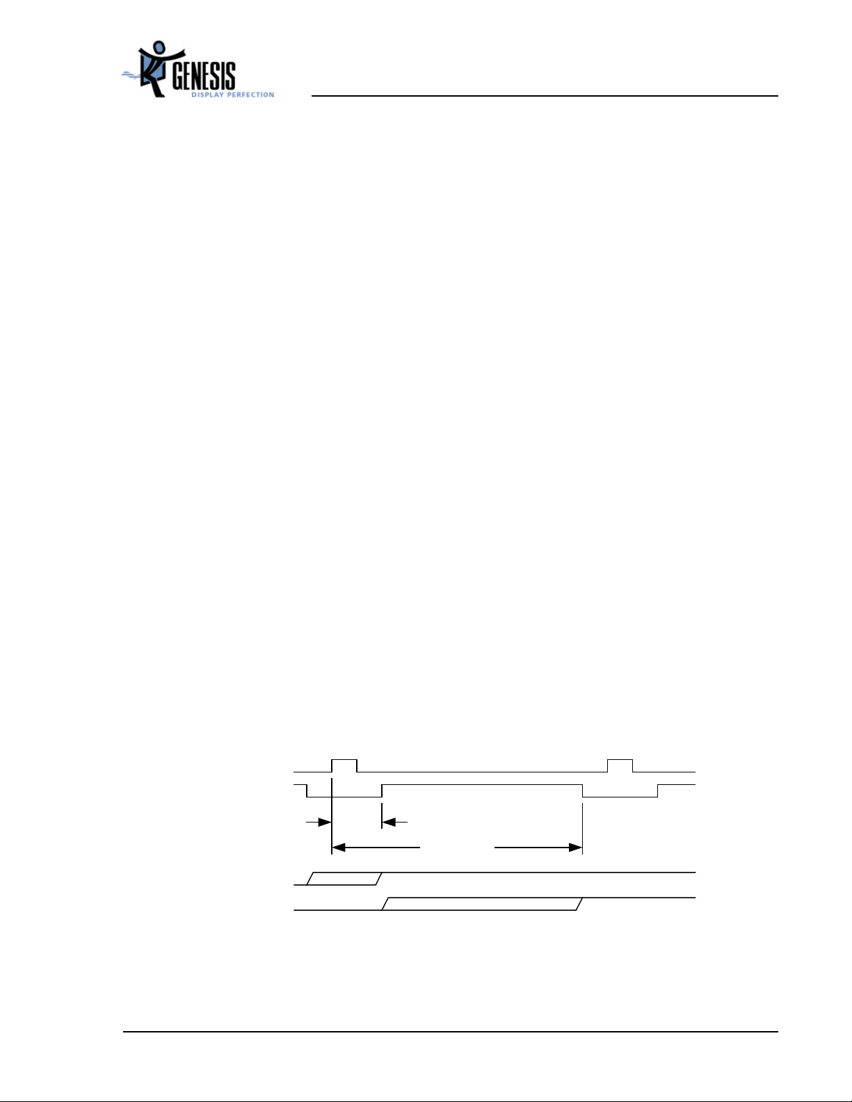
4.5.5 Internal Odd/Even Field Detection (For Interlaced Inputs to ADC Only)
The IFM has the ability to perform field decoding of interlaced inputs to the ADC. The user specifies start
and end values to outline a “window” relative to HSYNC. If the VSYNC leading edge occurs within this
window, the IFM signals the start of an ODD field. If the VSYNC leading edge occurs outside this
window, an EVEN field is indicated (the interpretation of odd and even can be reversed). The window
start and end points are selected from a predefined set of values.
HS
window
Window
Start
Window End
VS - even
VS - odd
Figure 18. ODD/EVEN Field Detection
C2121-DAT-01F 28 December 2002
http://www.genesis-microchip.com
Page 29
A
gm2121 Preliminary Data Sheet
4.5.6 Input Pixel Measurement
The gm2121 provides a number of pixel measurement functions intended to assist in configuring system
parameters such as pixel clock, SDDS sample clocks per line and phase setting, centering the image, or
adjusting the contrast and brightness.
4.5.7 Image Phase Measurement
This function measures the sampling phase quality over a selected active window region. This feature
may be used when programming the source DDS to select the proper phase setting. Please refer to the
gm2121 Programming Guide for the optimized algorithm.
4.5.8 Image Boundary Detection
The gm2121 performs measurements to determine the image boundary. This information is used when
programming the Active Window and centering the image.
4.5.9 Image Auto Balance
The gm2121 performs measurements on the input data that is used to adjust brightness and contrast.
4.6 RealColorTM Digital Color Controls
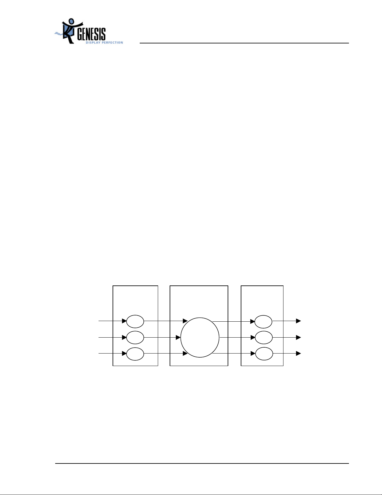
The gm2121 provides high-quality digital color controls. These consist of a subtractive "black level"
stage, followed by a full 3x3 RGB matrix multiplication stage, followed by a signed offset stage as shown
in Figure 19.
Red In
Green In
This structure can accommodate all RGB color controls such as black-level (subtractive stage), contrast
(multiplicative stage), and brightness (signed additive offset). In addition, it supports all YUV color
controls including brightness (additive factor applied to Y), contrast (multiplicative factor applied to Y),
hue (rotation of U and V through an angle) and saturation (multiplicative factor applied to both Y and V).
Blue In
Subtractive
Offset
(Black Level)
3x3 Color
Conversion
dditive
Offset
(Brightness)
-
-
X
-
+/
-
+/
-
-
Figure 19. RealColorTM Digital Color Controls
+/
Red Out
Green Out
Blue Out
To provide the highest color purity all mathematical functions use 10 bits of accuracy. The final result is
then dithered to eight or six bits (as required by the LCD panel).
C2121-DAT-01F 29 December 2002
http://www.genesis-microchip.com
Page 30

gm2121 Preliminary Data Sheet
4.6.1 RealColor™ Flesh tone Adjustment
The human eye is more sensitive to variations of flesh tones than other colors; for example, the user may
not care if the color of grass is modified slightly during image capture and/or display. However, if skin
tones are modified by even a small amount, it is unacceptable. The gm2121 features flesh tone
adjustment capabilities. This feature is not based on lookup tables, but rather a manipulation of
YUV-channel parameters. Flesh tone adjustment is available for all inputs.
4.6.2 Color Standardization and sRGB Support
Internet shoppers may be very picky about what color they experience on the display. gm2121
RealColor
TM
digital color controls can be used to make the color response of an LCD monitor compliant
with standard color definitions, such as sRGB. sRGB is a standard for color exchange proposed by
Microsoft and HP (see www.srgb.com)
. gm2121 RealColor controls can be used to make LCD monitors
sRGB compliant, even if the native response of the LCD panel itself is not.
4.7 High-Quality Scaling
The gm2121 zoom scaler uses an adaptive scaling technique proprietary to Genesis Microchip Inc., and
provides high quality scaling of real time video and graphics images. An input field/frame is scalable in
both the vertical and horizontal dimensions.
Interlaced fields may be spatially de-interlaced by vertically scaling and repositioning the input fields to
align with the output display’s pixel map.
4.7.1 Variable Zoom Scaling
The gm2121 scaling filter can combine its advanced scaling with a pixel-replication type scaling function.
This is useful for improving the sharpness and definition of graphics when scaling at high zoom factors
(such as VGA to SXGA).
4.7.2 Horizontal and Vertical Shrink
The gm2121 provides an arbitrary horizontal and vertical shrink down to (50% + 1 pixel/line) of the
original image size. This allows the gm2121 to capture and display images one VESA standard format
larger than the native display resolution. For example, UXGA may be captured and displayed on an
SXGA panel.
4.8 Bypass Options
The gm2121 has the capability to completely bypass internal processing. In this case, captured input
signals and data are passed, with a small register latency, straight through to the display output.
The gm2121 is also able to bypass the zoom filter.
C2121-DAT-01F 30 December 2002
http://www.genesis-microchip.com
Page 31

gm2121 Preliminary Data Sheet
4.9 Gamma LUT
The gm2121 provides an 8 to 10-bit look-up table (LUT) for each input color channel intended for
Gamma correction and to compensate for a non-linear response of the LCD panel. A 10-bit output results
in an improved color depth control. The 10-bit output is then dithered down to 8 bits (or 6 bits) per
channel at the display (see section 4.10.3 below). The LUT is user programmable to provide an arbitrary
transfer function. Gamma correction occurs after the zoom / shrink scaling block.
The LUT has bypass enable. If bypassed, the LUT does not require programming.
4.10 Display Output Interface
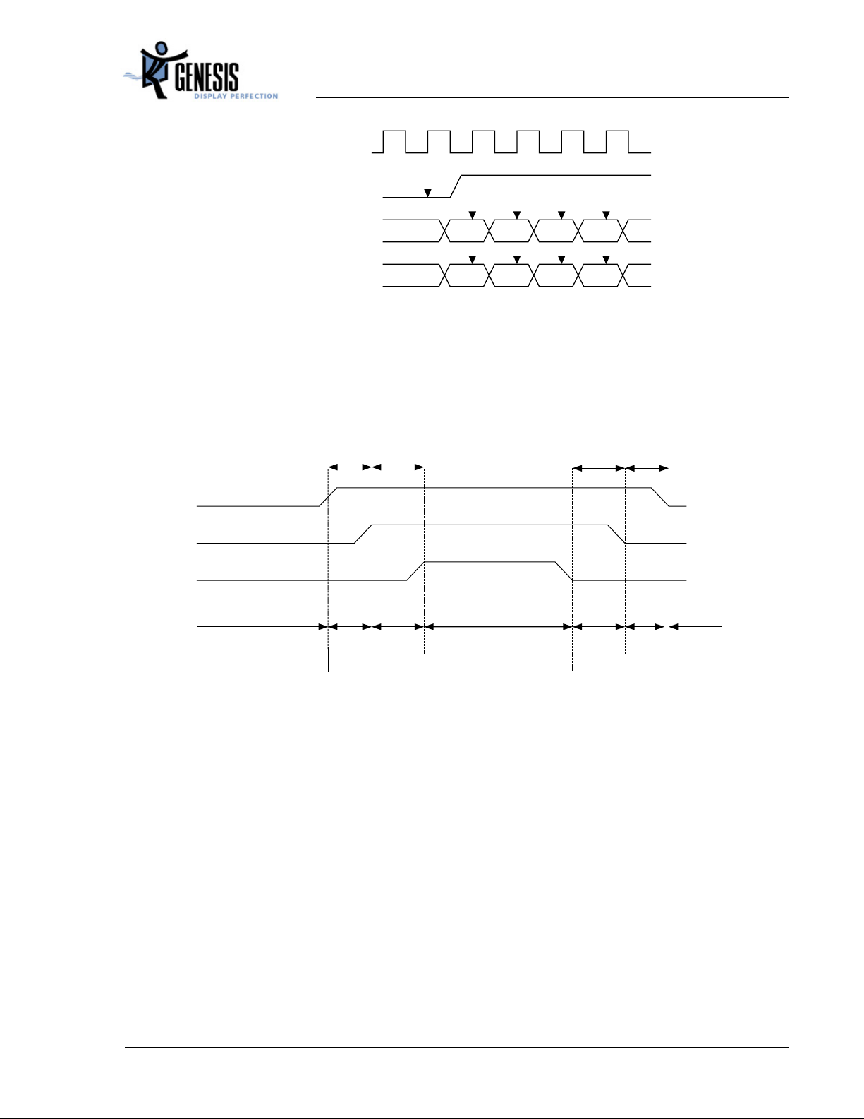
The Display Output Port provides data and control signals that permit the gm2121 to connect to a variety
of flat panel or CRT devices. The output interface is configurable for 18 or 24-bit RGB pixels, either
single or double pixel wide. All display data and timing signals are synchronous with the DCLK output
clock.
4.10.1 Display Synchronization
Refer to section 4.1 for information regarding internal clock synthesis.
The gm2121 supports the following display synchronization modes:
Frame Sync Mode: The display frame rate is synchronized to the input frame or field rate.
This mode is used for standard operation.
Free Run Mode: No synchronization. This mode is used when there is no valid input timing
(i.e. to display OSD messages or a splash screen) or for testing purposes. In free-run mode,
the display timing is determined only by the values programmed into the display window and
timing registers.
4.10.2 Programming the Display Timing
Display timing signals provide timing information so the Display Port can be connected to an external
display device. Based on values programmed in registers, the Display Output Port produces the
horizontal sync (DHS), vertical sync (DVS), and data enable (DEN) control signals, which are then
encoded into the LVDS data stream by the on-chip LVDS transmitter. The figure below provides the
registers that define the output display timing.
Horizontal values are programmed in single pixel increments relative to the leading edge of the horizontal
sync signal. Vertical values are programmed in line increments relative to the leading edge of the vertical
sync signal.
C2121-DAT-01F 31 December 2002
http://www.genesis-microchip.com
Page 32
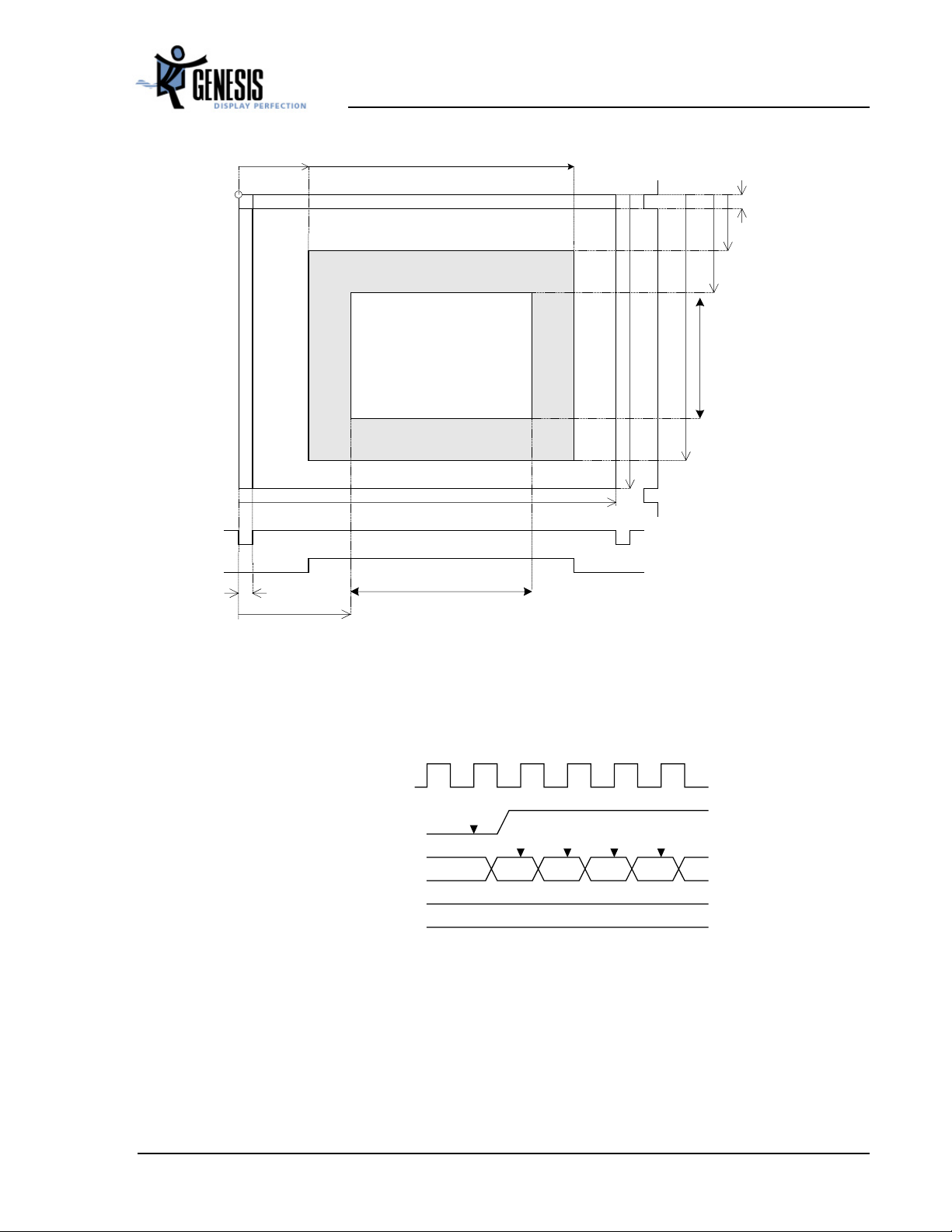
gm2121 Preliminary Data Sheet
DH_BKGND_START DH_BKGND_END
DVS
DHS
DEN **
HSYNC region
Horizontal Blanking (Back Porch)
DH_HS_END
DH_ACTIVE_START
Figure 20. Display Windows and Timing
VSYNC Region
Vertical Blanking (Back Porch)
Display Background Window
Display Active Window
Vertical Blanking (Front Porch)
DH_TOTAL
DH_ACTIVE_WIDTH
DV_BKGND_START
DV_ACTIVE_START
DV_ACTIVE_LENGTH
DV_TOTAL
Horizontal Blanking (Front Porch)
DV_BKGND_END
**
DEN is not asserted during vertical blanking
DV_VS_END
The double-wide output only supports an even number of horizontal pixels.
DCLK (Output )
DEN (Output )
ER/EG/EB
(Output )
OR/OG/ OB
(Output )
XXX
rgb0 rgb4rgb3rgb2rgb1
XXX
Figure 21. Single Pixel Width Display Data
C2121-DAT-01F 32 December 2002
http://www.genesis-microchip.com
Page 33
gm2121 Preliminary Data Sheet
DCLK (Output )
DEN (Output)
ER/EG/EB
(Output)
OR/OG/OB
(Output)
XXX
XXX
rgb0 rgb8rgb6rgb4rgb2
rgb1 rgb9rgb7rgb5rgb3
Figure 22. Double Pixel Wide Display Data
4.10.3 Panel Power Sequencing (PPWR, PBIAS)
gm2121 has two dedicated outputs PPWR and PBIAS to control LCD power sequencing once data and
control signals are stable. The timing of these signals is fully programmable.
TMG1 TMG2 TMG2 TMG1
PPWR Output
Panel Data and Control Signals
PBIAS Output
<State0> <State1> <State2> <State3> <State2> <State1> <State0>
POWER_SEQ_EN = 1 POWER_SEQ_EN = 0
Figure 23. Panel Power Sequencing
4.10.4 Output Dithering
The Gamma LUT outputs a 10-bit value for each color channel. This value is dithered down to either 8bits for 24-bit per pixel panels, or 6-bits for 18-bit per pixel panels.
The benefit of dithering is that the eye tends to average neighboring pixels and a smooth image free of
contours is perceived. Dithering works by spreading the quantization error over neighboring pixels both
spatially and temporally. Two dithering algorithms are available: random or ordered dithering. Ordered
dithering is recommended when driving a 6-bit panel.
All gray scales are available on the panel output whether using 8-bit panel (dithering from 10 to 8 bits per
pixel) or using 6-bit panel (dithering from 10 down to 6 bits per pixel).
C2121-DAT-01F 33 December 2002
http://www.genesis-microchip.com
Page 34
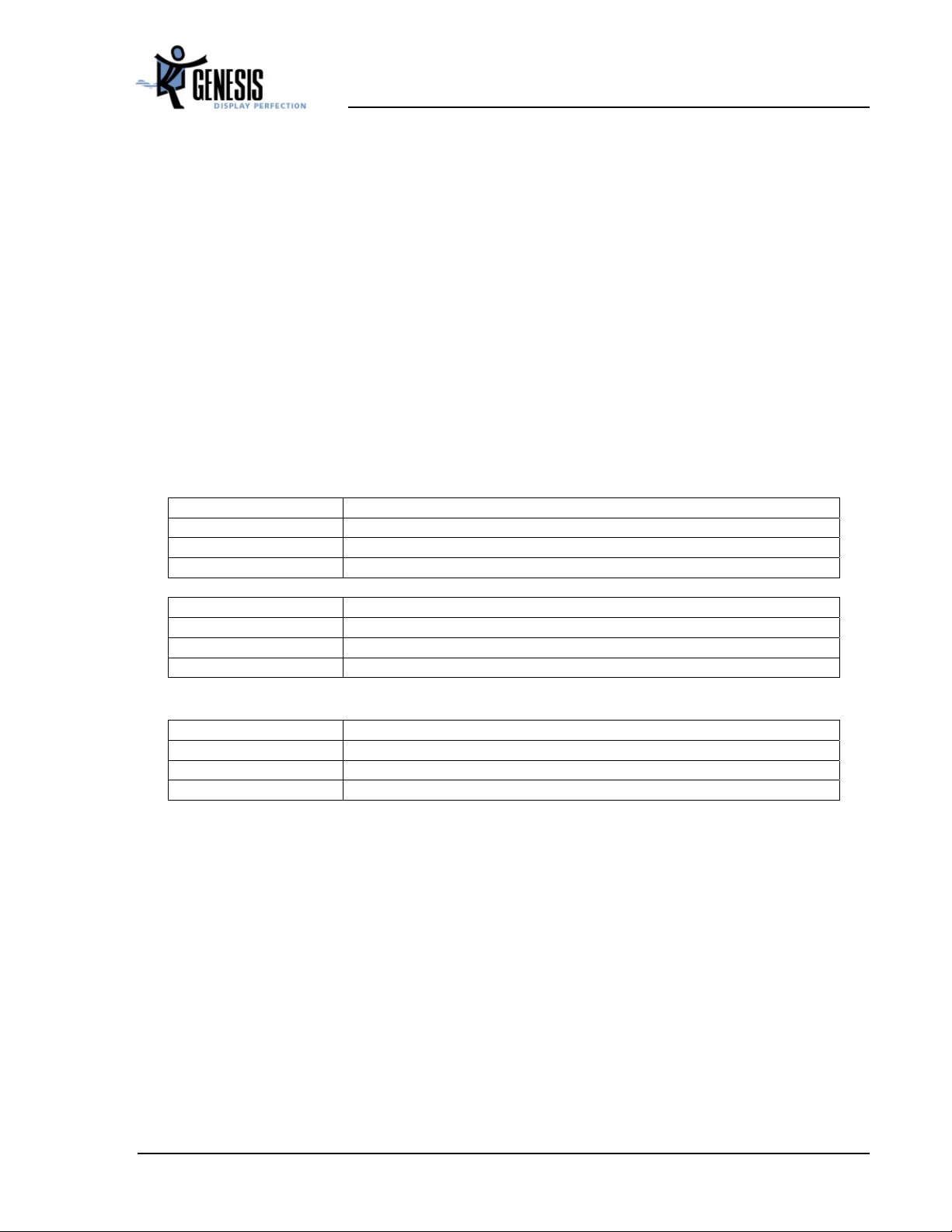
gm2121 Preliminary Data Sheet
4.11 Dual Four Channel LVDS Transmitter
The gm2121 implements the industry standard flexible four channel dual LVDS transmitter. The LVDS
transmitter can support the following:
• Single or double pixel mode
• 24/48-bit panel mapping to the LVDS channels (see Table 14)
• 18/36-bit panel mapping to the LVDS channels (see Table 15)
• Programmable even/odd LVDS swapping
• Programmable channel swapping (the clocks are fixed)
• Programmable channel polarity swapping
• Support up to SXGA 75Hz output
Table 14. Supported LVDS 24-bit Panel Data Mapping
Channel 0 R0, R1, R2, R3, R4, R5, G0
Channel 1 G1, G2, G3, G4, G5, B0, B1
Channel 2 B2, B3, B4, B5, PHS, PVS, PDE
Channel 3 R6, R7, G6, G7, B6, B7, RES
Channel 0 R2, R3, R4, R5, R6, R7, G2
Channel 1 G3, G4, G5, G6, G7, B2, B3
Channel 2 B4, B5, B6, B7, PHS, PVS, PDE
Channel 3 R0, R1, G0, G1, B0, B1, RES
Table 15. Supported LVDS 18-bit Panel Data Mapping
Channel 0 R0, R1, R2, R3, R4, R5, G0
Channel 1 G1, G2, G3, G4, G5, B0, B1
Channel 2 B2, B3, B4, B5, PHS, PVS, PDE
Channel 3 Disabled for this mode
4.12 Energy Spectrum Management (ESM)
High spikes in the EMI power spectrum may cause LCD monitor products to violate emissions standards.
The gm2121 has many features that can be used to reduce electromagnetic interference (EMI). These
include drive strength control, dual-edge clocking and clock spectrum modulation. These features help to
eliminate the costs associated with EMI reducing components and shielding.
4.13 OSD
The gm2121 has a fully programmable, high-quality OSD controller. The graphics are divided into “cells”
12 by 18 pixels in size. The cells are stored in an on-chip static RAM (4096 words by 24 bits) and can be
C2121-DAT-01F 34 December 2002
http://www.genesis-microchip.com
Page 35
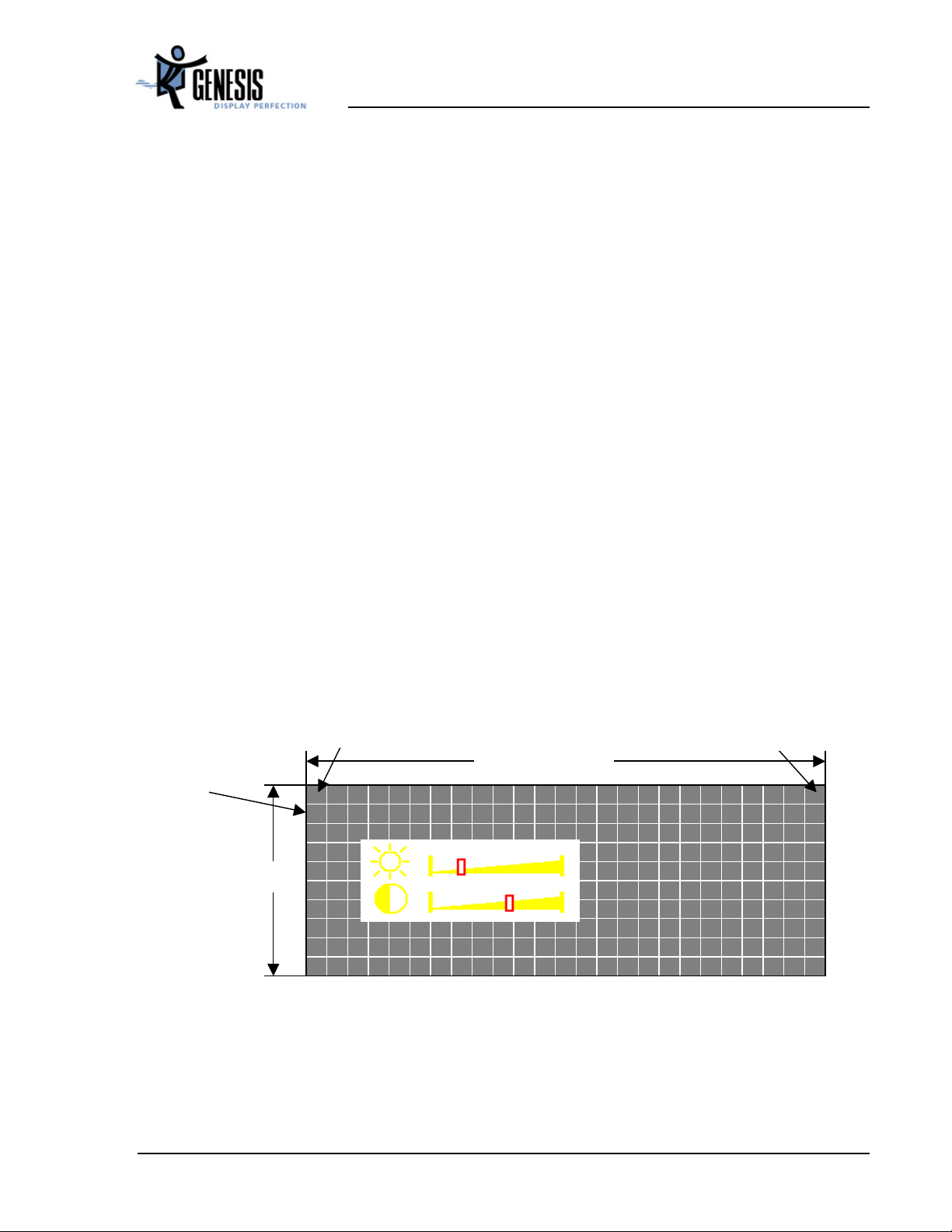
gm2121 Preliminary Data Sheet
stored as 1-bit per pixel data, 2-bit per pixel data or 4-bit per pixel data. This permits a good compression
ratio while allowing more than 16 colors in the image.
Some general features of the gm2121 OSD controller include:
OSD Position – The OSD menu can be positioned anywhere on the display region. The reference point is
Horizontal and Vertical Display Background Start (DH_BKGND_START and DV_BKGND_START in
Figure 20).
OSD Stretch – The OSD image can be stretched horizontally and/or vertically by a factor of two, three,
or four. Pixel and line replication is used to stretch the image.
OSD Blending – Sixteen levels of blending are supported for the character-mapped and bitmapped
images. One host register controls the blend levels for pixels with LUT values of 128 and greater,
while another host register controls the blend levels for pixels with LUT values of 127 and lower.
OSD color LUT value 0 is reserved for transparency and is unaffected by the blend attribute.
4.13.1 On-Chip OSD SRAM
Address26:
Cell attributes for
st
1
The on-chip static RAM (4096 words by 24 bits) stores the cell map and the cell definitions.
In memory, the cell map is organized as an array of words, each defining the attributes of one visible
character on the screen starting from upper left of the visible character array. These attributes specify
which character to display, whether it is stored as 1, 2 or 4 bits per pixel, the foreground and background
colors, blinking, etc.
Registers CELLMAP_XSZ and CELLMAP_YSZ are used to define the visible area of the OSD image.
For example, Figure 24 shows a cell map for which CELLMAP_XSZ =25 and CELLMAP_YSZ =10.
cell, 2nd row
CELLMAP_YS
Address 1:
Cell Attributes for
upper-left hand cell
CELLMAP_XSZ
Brightness
Address 25:
Attributes for
upper-right hand cell
Contrast
Figure 24. OSD Cell Map
Cell definitions are stored as bit map data. On-chip registers point to the start of 1-bit per pixel
definitions, 2-bit per pixel definitions and 4-bit per pixel definitions respectively. 1, 2 and 4-bit per pixel
cell definitions require 9, 18 and 36 words of the OSD RAM respectively.
C2121-DAT-01F 35 December 2002
http://www.genesis-microchip.com
Page 36

gm2121 Preliminary Data Sheet
Note that the cell map and the cell definitions share the same on-chip RAM. Thus, the size of the cell map
can be traded off against the number of different cell definitions. In particular, the size of the OSD image
and the number of cell definitions must fit in OSD SRAM. That is, the following inequality must be
satisfied. (Note, the ROUND operation rounds 3.5 to 4).
(CELLMAP_XSZ+1) * CELLMAP_YSZ +
18 * ROUND(Number of 1-bit per pixel fonts / 2) +
18 * (Number of 2-bit per pixel fonts) +
36 * (Number of 4-bit per pixel fonts) <= 4096
For example, an OSD menu 360 pixels wide by 360 pixels high is 30 cells in width and 20 cells in height.
Many of these cells would be the same (e.g. empty). In this case, the menu could contain more than 32 1bit per pixel cells, 100 2-bit per pixel cells, and 16 4-bit per pixel cells. Of course, different numbers of
each type can also be used.
4.13.2 Color Look-up Table (LUT)
Each pixel of a displayed cell is resolved to an 8-bit color code. This selected color code is then
transformed to a 24-bit value using a 256 x 24-bit look up table. This LUT is stored in an on-chip RAM
that is separate from the OSD RAM. Color index value 0x00 is reserved for transparent OSD pixels.
4.14 On-Chip Microcontroller (OCM)
The gm2121 on-chip microcontroller (OCM) serves as the system microcontroller. It programs the
gm2121 and manages other devices in the system such as the keypad, the back light and non-volatile
RAM (NVRAM) using general-purpose input/output (GPIO) pins.
The OCM can operate in two configurations, Standalone configuration and Full-Custom configuration, as
illustrated in Figure 25.
C2121-DAT-01F 36 December 2002
http://www.genesis-microchip.com
Page 37
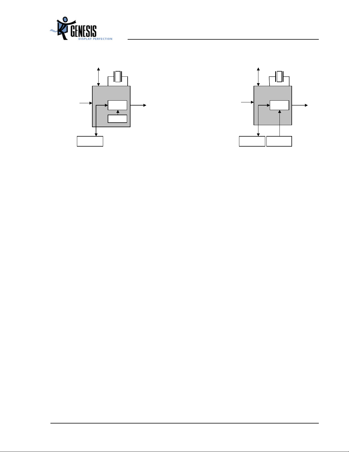
Factory
Port
Analog
RGB
Input
NVRAM
Configuration settings in NVRAM
•
OSD Colors, Logo and other configuration
•
Panel Parameters
•
Additional input modes
•
Code patches
gm2121
Figure 1. OCM Full-Custom and Standalone Configurations
OCM
ROM
Output to
LCD Panel
On-chip ROM
•
Auto mode detection
•
Auto-configuration
•
Standard high-quality OSD menus
•
Factory test / calibration functions
:
:
gm2121 Preliminary Data Sheet
Factory
Port
Analog
RGB
Input
NVRAM
User settings in NVRAM
•
Brightness/contrast settings, etc
•
On mode-by-mode basis
gm2121
:
OCM
PROM
External ROM
•
Contains firmware code and data
for all firmware functions
Output to
LCD Panel
:
A - Standalone Configuration
(No external ROM)
B - Full-Custom Configuration
(Program and Data stored in external ROM)
Figure 25. OCM Full-Custom and Standalone Configurations
4.14.1 Standalone Configuration
Standalone configuration offers the most simple and inexpensive system solution for generic LCD
monitors. In this configuration the OCM executes firmware stored internally in gm2121. The baud rate
for serial communication (in standalone configuration) is determined by two bootstrap resistors on
ROMADDR11 (TCLK_SEL1, pin 145) and ROMADDR10 (TCLK_SEL0, pin 146). The on-chip
firmware provides all the standard functions required in a high-quality generic LCD monitor. This
includes mode-detection, auto-configuration and a high-quality standard OSD menu system. No external
ROM is required (which reduces BOM cost) and no firmware development effort is required (which
reduces time-to-market).
In Standalone configuration many customization parameters are stored in NVRAM. These include the
LCD panel timing parameters, the color scheme and logos used in the OSD menus, the functions provided
by the OSD menus, and arbitrary firmware modifications. These customization parameters are described
in the Standalone User’s Guide (B0108-SUG-01). Based on the customization parameters, G-Wizard (a
GUI-based development tool used to program Genesis devices) produces the hex image file for NVRAM.
G-Probe is then used to download the NVRAM image file into the NVRAM device. This is illustrated in
Figure 26 below.
C2121-DAT-01F 37 December 2002
http://www.genesis-microchip.com
Page 38
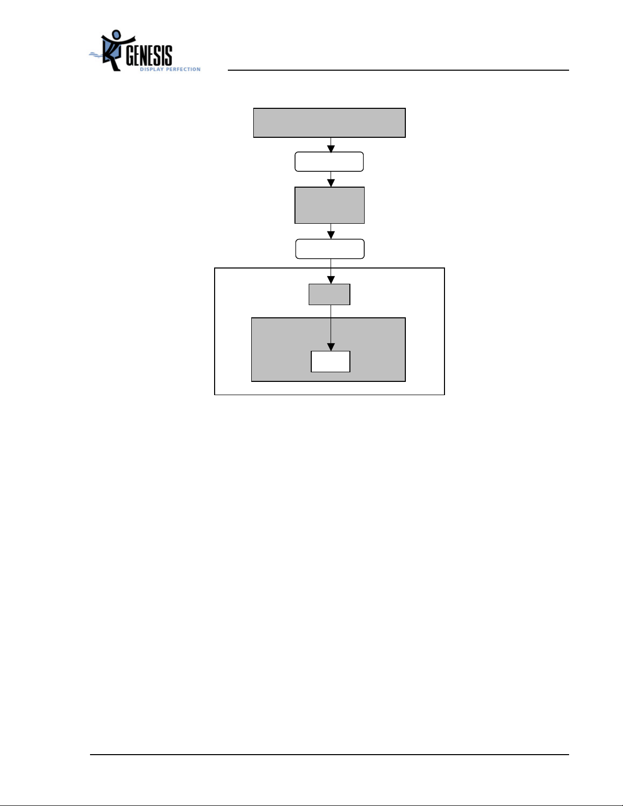
gm2121 Preliminary Data Sheet
Specify Configurable Parameters
(See Standalone Users Guide)
G-Wizard
NVRAM
Image File
(.nvram_image. hex)
G-Probe
LCD
Controller
Board
NVRAM
gm2121
OCM
Figure 26. Programming OCM in Standalone Configuration
4.14.2 Full-Custom Configuration
In full-custom configuration the OCM executes a firmware program running from external ROM. A
parallel port with separate address and data busses is available for this purpose. This port connects
directly to standard, commercially available ROM or programmable Flash ROM devices. Normally 64KB
or 128KB of ROM is required.
Both instructions and data are fetched from external ROM on a cycle-by-cycle basis. The external ROM
access speed on the parallel port is determined by the gm2121 internal OCM_CLK, which is derived from
the TCLK. As a result, the external ROM device’s access speed requirements are directly related to the
TCLK frequency. For the detailed timing requirements see section 5.3 “External ROM Interface Timing
Requirements”).
To program gm2121 in full-custom configuration the content of the external ROM is generated using
Genesis software development tools G-Wizard and OSD-Workbench. This is illustrated in Figure 27. GWizard is a GUI-based tool for capturing system information such as panel timing, support modes, system
configuration, etc. OSD-Workbench is a GUI based tool for defining OSD menus and functionality.
C2121-DAT-01F 38 December 2002
http://www.genesis-microchip.com
Page 39
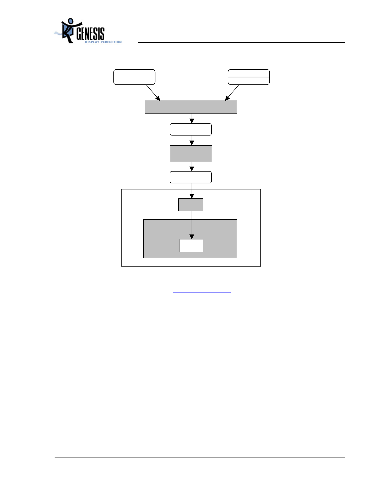
gm2121 Preliminary Data Sheet
G-Wizard
gm2121 Driver
OSD Workbench
gm2121 Driver
Firmware source files (*.c *.h)
Keil Compiler
External ROM
Image File (.hex)
ROM Programmer
LCD
Controller
Board
ROM
gm2121
OCM
Figure 27. Programming the OCM in Full-Custom Configuration
Genesis recommends using Keil compiler (http://www.keil.com/) to compile the firmware source code
into a hex file. This hex file is then downloaded into the external ROM using commercially available
ROM programmers.
For development purposes it may be useful to use a ROM emulator. For example, a PROMJET ROM
emulator can be used (http://www.emutec.com/pjetmain.html)
4.14.3 In-System-Programming (ISP) of FLASH ROM Devices
Gm2121 has hardware to program FLASH ROM devices. In particular, the GPIO11/ROM_WEn pin can
be connected to the write enable of the FLASH ROM. Firmware is then used to perform the writes using
the gm2121host registers.
4.14.4 UART Interface
.
The gm2121 OCM has an integrated Universal Asynchronous Remote Terminal (UART) port that can be
used as a factory debug port. In particular, the UART can be used to 1) read / write chip registers, 2) read
/ write to NVRAM, and 3) read / write to FLASH ROM.
C2121-DAT-01F 39 December 2002
http://www.genesis-microchip.com
Page 40

gm2121 Preliminary Data Sheet
The UART is connected to pins GPIO4/UART_DI and GPIO5/UART_DO. gm2121 has serial-toparallel conversion hardware which is accessed by firmware.
Note: Install 10KΩ pull-ups on UART according to Table 3.
4.14.5 DDC2Bi Interface
The gm2121 also features hardware support for DDC2Bi communication over the DDC channel of the
analog input ports. The specification for the DDC2Bi standard can be obtained from VESA
(www.vesa.org)
. The DDC2Bi port can be used as a factory debug port or for field programming. In
particular, the DDC2Bi port can be used to 1) read / write chip registers (see section 4.15 below), 2) read /
write to NVRAM (see section 4.13.1 above), and 3) read / write to FLASH ROM (see section 4.13.3
above).
For DDC2Bi communication over the analog VGA connector pins GPIO22/HCLK and GPIO16/HFSn
should be connected to the DDC clock and data pins of the analog DSUB15 VGA connector. gm2121
contains serial to parallel conversion hardware, that is then accessed by firmware for interpretation and
execution of the DDC2Bi command set. Bootstrap option ROM_ADDR12 (pin 142) is used to select the
pin pair to be used for DDC2Bi communication. This signal (named DDC_PORT_SEL) selects between
DDC2Bi interface or GPIO functions for pin pairs 8 (GPIO22/HCLK), 9 (GPIO16/HFSn) and 18
(GPIO15/DDC_SCL), 19 (GPIO14/DDC_SDA) for the internal standalone firmware. See the truth table
below for further details.
DDC2Bi
Pin pair
Pin pair
HFSn / HCLK
Pin pair
DDC_SDA /
DDC_SCL
Pin number
(Port Function)
Pin 8
(GPIO22/HCLK)
Pin 9
(GPIO16/HFSn)
Pin 18
(GPIO15/DDC_SCL)
Pin 19
(GPIO14/DDC_SDA)
DDC_PORT_SEL = ’0’
ROM_ADDR12 (pin
142) pulled LOW
GPIO22 HCLK
GPIO16 HFSn
DDC_SCL GPIO15
DDC_SDA GPIO14
DDC_PORT_SEL = ’1’
ROM_ADDR12 (pin
142) pulled HIGH
4.14.6 General Purpose Inputs and Outputs (GPIO’s)
The gm2121 has 23 general-purpose input/output (GPIO) and 8 general-purpose output (GPO) pins.
These are used by the OCM to communicate with other devices in the system such as keypad buttons,
NVRAM, LEDs, audio DAC, etc. Each GPIO has independent direction control, open drain enable, for
reading and writing. The GPO’s are shared with gm2121’s TEST_BUS. To activate these GPO’s set
TEST BUS_CONTROL (register 0x1E6) to 0x00 and TEST_BUS_EN (register 0x1E7 bit 2) to ‘1’, pins
88-97 can function as general-purpose outputs GPO0-7. Note that the GPIO pins have alternate
functionality as described in Table 16 below.
C2121-DAT-01F 40 December 2002
http://www.genesis-microchip.com
Page 41
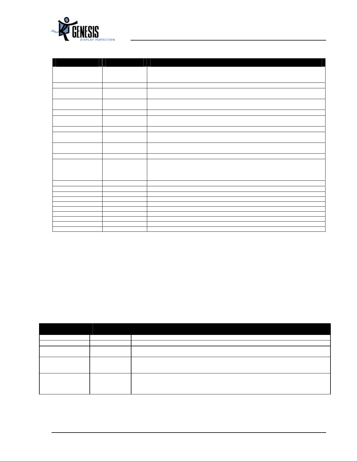
gm2121 Preliminary Data Sheet
Table 16. gm2121 GPIOs and Alternative Functions
Pin Name Pin Number Alternative function
GPIO0/PWM0
GPIO1/PWM1
GPIO2/PWM2
GPIO3/TIMER1 26 Timer1 input of the OCM.
GPIO4/UART_DI
GPIO5/UARD_D0
GPIO6
GPIO7
GPIO8/IRQINn 22 OCM external interrupt source (IRQINn).
GPIO9
GPIO10
GPIO11/ROM_WEn 35 Write enable for external ROM if programmable FLASH device is used.
GPIO12/NVRAM_SDA
GPIO13/NVRAM_SCL
GPIO14/DDC_SCL
GPIO15/DDC_SDA
GPIO16/HFSn 9 Serial data line for 2-wire host interface.
GPIO17/HDATA0
GPIO18/HDATA1
GPIO19/HDATA2
GPIO20/HDATA3
GPIO21/IRQn 16 OCM interrupt output pin.
GPIO22/HCLK 8 Serial input clock for 2-wire host interface.
GPO 0 88
GPO 1 89
GPO 2 92
GPO 3 93
GPO 4 94
GPO 5 95
GPO 6 96
GPO 7 97
23
24
25
27
28
29
32
33
34
36
37
18
19
13
12
11
10
PWM0, PWM1 and PWM2 back light intensity controls, as described in section 4.17.2 below.
OCM UART data in/out signals respectively.
Data and clock lines for master 2-wire serial interface to NVRAM when gm2121 is used in standalone
configuration (section 4.14.1).
General-purpose input/output signals. Open drain option via register setting.
[Bi-directional Input, Schmitt trigger (400mV typical hysteresis), 5V-tolerant]
4.15 Bootstrap Configuration Pins
During hardware reset, the external ROM address pins ROM_ADDR[15:0] are configured as inputs. On
the negating edge of RESETn, the value on these pins is latched and stored. This value is readable by the
on-chip microcontroller (or an external microcontroller via the host interface). Install a 10K pull-up
resistor to indicate a ‘1’, otherwise a ‘0’ is indicated because ROM_ADDR[15:0] have a 60KΩ internal
pull-down resistor.
Table 17. Bootstrap Signals
Signal Name Pin Name Description
HOST_ADDR(6:0) ROM_ADDR(6:0) If using 2-wire host protocol, these are the serial bus device address.
HOST_PROTOCOL ROM_ADDR7 Program this bit to 0 for 2-wire host interface operation.
HOST_PORT_EN ROM_ADDR8 Program this bit to 0 for 2-wire host interface operation.
OCM_START ROM_ADDR9 Determines the operating condition of the OCM after HW reset:
DDC_PORT_SEL ROM_ADDR12 Selects the pin pair to be used for DDC2Bi communication for the standalone firmware (standalone
Note: For DDC2Bi operation on HCLK/HFSn (recommended) set to 0 (unconnected).
0 = OCM remains in reset until enabled by register bit.
1 = OCM becomes active after OCM_CLK is stable.
configuration is selected when bootstrap of ROM_ADDR14 = 0)
0 = GPIO14/DDC_SCL and GPIO15/DDC_SDA
1 = GPIO22/HCLK and GPIO16/HFSn
C2121-DAT-01F 41 December 2002
http://www.genesis-microchip.com
Page 42

gm2121 Preliminary Data Sheet
Signal Name Pin Name Description
TCLK_SEL1
TCLK_SEL0
OSC_SEL ROM_ADDR13 Selects reference clock source (refer to Figure 7):
OCM_ROM_CNFG(1) ROM_ADDR14 Together with OCM_CONTROL register (0x22) bit 4, this bit selects internal/external ROM configuration.
PBIAS_POL ROM_ADDR15 Sets the polarity of the PBIAS signal after the RESET sequence. This is to prevent flashing during power
ROM_ADDR11
ROM_ADDR10
Selects the for the standalone firmware UART baud rate depending on the frequency of the TCLK crystal
(TCLK_SEL1, TCLK_SEL0)
00 = 115.2 KBaud (for TCLK = 14.3 MHz)
01 = 57.6 KBaud (for TCLK = 20 MHz)
10 = 57.6 KBaud (for TCLK = 24 MHz)
11 = 57.6 KBaud (for TCLK = 14.3 MHz)
0 = XTAL and TCLK pins are connected to a crystal oscillator.
1 = TCLK input is driven with a single-ended TTL/CMOS clock oscillator.
0 = All 48K of ROM is internal.
1 = All 48K of ROM is in external ROM using ROM_ADDR15:0 address outputs if
register 0x22 bit 4 is 0. If register 0x22 bit 4 is 1, 0-32K ROM is internal, and
32K~48K ROM is external using ROM_ADDR13:0 address outputs.
Note: When booting from internal ROM (standalone configuration) the embedded firmware checks for a
signature in external ROM (values 0x89, 0xAB, 0xCD, 0xEF at addresses 0xFFFC, 0xFFFD, 0xFFFE,
0xFFFF) and if present then OCM begins executing from address 0x0000 of external ROM (i.e. full-custom
configuration).
up, for panels with active LOW panel enable signal.
0 = PBIAS set to LOW after RESET
1 = PBIAS set to HIGH after RESET
4.16 Host Interface
gm2121 contains many internal registers that control its operation. These are described in the gm2121
Register Listing (C2121-DSL-01).
A serial host interface is provided to allow an external device to peek and poke registers in the gm2121.
This is done using a 2-wire serial protocol. Note that 2-wire host interface requires bootstrap settings as
described in Table 17.
An arbitration mechanism ensures that register accesses from the OCM and the 2-wire host interface port
are always serviced (time division multiplexing).
4.16.1 Host Interface Command Format
Transactions on the 2-wire host protocol occurs in integer multiples of bytes (i.e. 8 bits or two nibbles
respectively). These form an instruction byte, a device register address and/or one or more data bytes.
This is described in Table 18.
The first byte of each transfer indicates the type of operation to be performed by the gm2121. The table below
lists the instruction codes and the type of transfer operation. The content of bytes that follow the instruction byte
will vary depending on the instruction chosen. By utilizing these modes effectively, registers can be quickly
configured.
The two LSBs of the instruction code, denoted 'A9' and 'A8' in Table 18 below, are bits 9 and 8 of the
internal register address respectively. Thus, they should be set to ‘00’ to select a starting register address
of less than 256, ‘01’ to select an address in the range 256 to 511, and '10' to select an address in the range
512 to 767. These bits of the address increment in Address Increment transfers. The unused bits in the
instruction byte, denoted by 'x', should be set to ‘1’.
C2121-DAT-01F 42 December 2002
http://www.genesis-microchip.com
Page 43
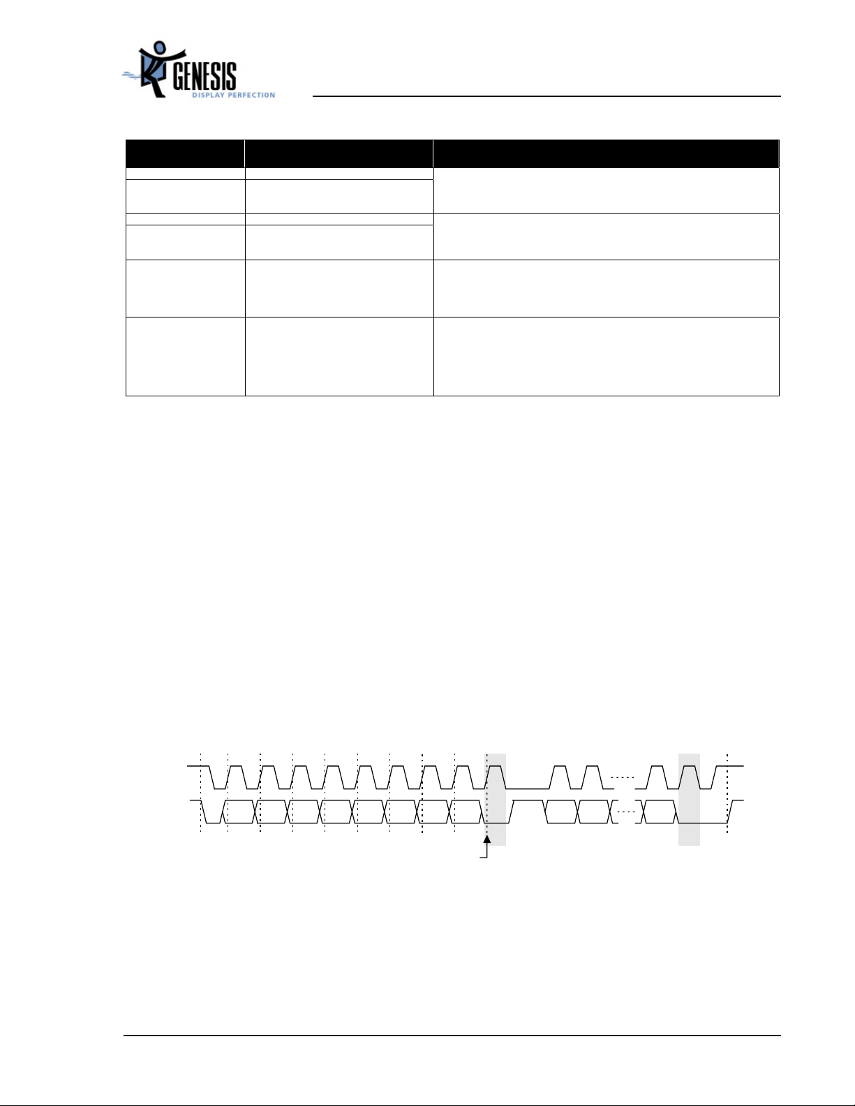
Bit
7 6 5 4 3 2 1 0
0 0 0 1 x x A9 A8 Write Address Increment
0 0 1 0 x x A9 A8 Write Address No Increment
1 0 0 1 x x A9 A8 Read Address Increment
1 0 1 0 x x A9 A8 Read Address No Increment
0 0 1 1 x x A9 A8
0 1 0 0 x x A9 A8
1 0 0 0 x x A9 A8
1 0 1 1 x x A9 A8
1 1 0 0 x x A9 A8
0 0 0 0 x x A9 A8
0 1 0 1 x x A9 A8
0 1 1 0 x x A9 A8
0 1 1 1 x x A9 A8
1 1 0 1 x x A9 A8
1 1 1 0 x x A9 A8
1 1 1 1 x x A9 A8
Operation Mode Description
(for table loading)
(for table reading)
Reserved
Spare No operation will be performed
4.16.2 2-wire Serial Protocol
Table 18. Instruction Byte Map
Allows the user to write a single or multiple bytes to a specified starting
address location. A Macro operation will cause the internal address pointer to
increment after each byte transmission. Termination of the transfer will cause
the address pointer to increment to the next address location.
Allows the user to read multiple bytes from a specified starting address
location. A Macro operation will cause the internal address pointer to
increment after each read byte. Termination of the transfer will cause the
address pointer to increment to the next address location.
gm2121 Preliminary Data Sheet
The 2-wire protocol consists of a serial clock HCLK and bi-directional serial data line HFSn. The bus
master drives HCLK and either the master or slave can drive the HFSn line (open drain) depending on
whether a read or write operation is being performed. The gm2121 operates as a slave on the interface.
The 2-wire protocol requires each device be addressable by a 7-bit identification number. The gm2121 is
initialized on power-up to 2-wire mode by asserting bootstrap pins HOST_PROTOCOL=0 and the device
identification number on HOST_ADDR(6:0) on the rising edge of RESETn (see Table 17). This provides
flexibility in system configuration with multiple devices that can have the same address.
A 2-wire data transfer consists of a stream of serially transmitted bytes formatted as shown in the figure
below. A transfer is initiated (START) by a high-to-low transition on HFSn while HCLK is held high. A
transfer is terminated by a STOP (a low-to-high transition on HFSn while HCLK is held high) or by a
START (to begin another transfer). The HFSn signal must be stable when HCLK is high, it may only
change when HCLK is low (to avoid being misinterpreted as START or STOP).
HCLK
HFSn
START
123 789
Receiver acknowledges by holding SDA low
456 12 89
ACK
R/WA6 A1A2A3A4A5 A0 D6D7 D0
ADDRESS BYTE
DATA BYTE
ACK
STOP
Figure 28. 2-Wire Protocol Data Transfer
Each transaction on the HFSn is in integer multiples of 8 bits (i.e. bytes). The number of bytes that can be
transmitted per transfer is unrestricted. Each byte is transmitted with the most significant bit (MSB) first.
After the eight data bits, the master releases the HFSn line and the receiver asserts the HFSn line low to
C2121-DAT-01F 43 December 2002
http://www.genesis-microchip.com
Page 44
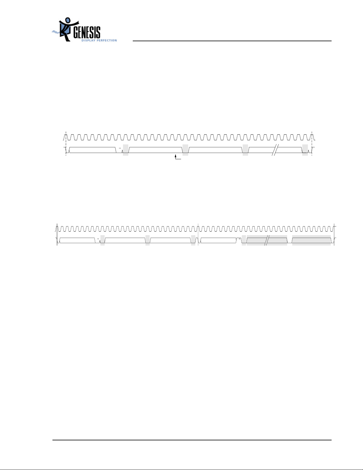
gm2121 Preliminary Data Sheet
acknowledge receipt of the data. The master device generates the HCLK pulse during the acknowledge
cycle. The addressed receiver is obliged to acknowledge each byte that has been received.
The Write Address Increment and the Write Address No Increment operations allow one or multiple
registers to be programmed with only sending one start address. In Write Address Increment, the address
pointer is automatically incremented after each byte has been sent and written. The transmission data
stream for this mode is illustrated in Figure 29 below. The highlighted sections of the waveform represent
moments when the transmitting device must release the HFSn line and wait for an acknowledgement from
the gm2121 (the slave receiver).
HCLK
123456789
HFSn
START
DEVICE ADDRES S REGISTER ADDRESS DATA DATAR/W
123456789
ACK OPERATION CODE
A9
12345678912 9
A8
Two MSBs of r egister addr ess
ACKACK
ACK
STOP
Figure 29. 2-Wire Write Operations (0x1x and 0x2x)
The Read Address Increment (0x90) and Read Address No Increment (0xA0) operations are illustrated in
Figure 30. The highlighted sections of the waveform represent moments when the transmitting device
must release the HFSn line and waits for an acknowledgement from the master receiver.
Note that on the last byte read, no acknowledgement is issued to terminate the transfer.
HCLK
HFSn
DEVICE ADDRESS REGISTER ADDRESSR/W ACK R/W ACK ACK
START
OPERATION CODE
ACKACK
START
DATADEVICE ADDRESS DATADATA
Figure 30. 2-Wire Read Operation (0x9x and 0xAx)
Please note that in all the above operations the operation code includes two address bits, as described in
Table 18.
STOP
4.17 Miscellaneous Functions
4.17.1 Low Power State
The gm2121 provides a low power state in which the clocks to selected parts of the chip may be disabled (see
Table 20).
C2121-DAT-01F 44 December 2002
http://www.genesis-microchip.com
Page 45

gm2121 Preliminary Data Sheet
4.17.2 Pulse Width Modulation (PWM) Back Light Control
Many of today’s LCD back light inverters require both a PWM input and variable DC voltage to
minimize flickering (due to the interference between panel timing and inverter’s AC timing), and adjust
brightness. Most LCD monitor manufactures currently use a microcontroller to provide these control
signals. To minimize the burden on the external microcontroller, the gm2121 generates these signals
directly.
There are three pins available for controlling the LCD back light, PWM0 (GPIO0), PWM1 (GPIO1) and
PWM2 (GPIO2). The duty cycle of these signals is programmable. They may be connected to an external
RC integrator to generate a variable DC voltage for a LCD back light inverter. Panel HSYNC is used as
the clock for a counter generating this output signal.
C2121-DAT-01F 45 December 2002
http://www.genesis-microchip.com
Page 46
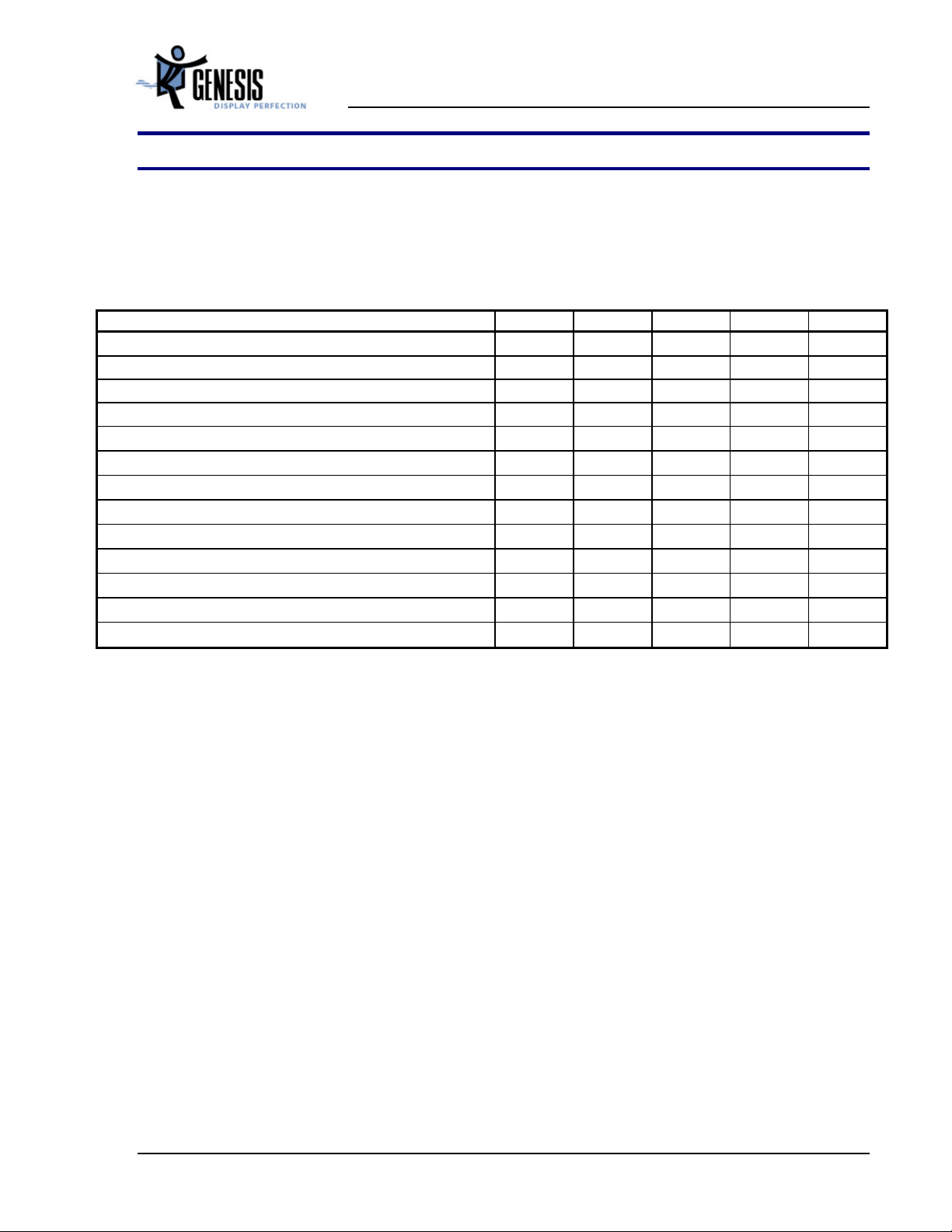
gm2121 Preliminary Data Sheet
5 Electrical Specifications
The following targeted specifications have been derived by simulation.
5.1 Preliminary DC Characteristics
Table 19. Absolute Maximum Ratings
PARAMETER SYMBOL MIN TYP MAX UNITS
3.3V Supply Voltages
2.5V Supply Voltages
Input Voltage (5V tolerant inputs)
Input Voltage (non 5V tolerant inputs)
Electrostatic Discharge V
Latch-up ILA
Ambient Operating Temperature TA 0 70
Storage Temperature T
Operating Junction Temp. TJ 0 125
Thermal Resistance (Junction to Air) Natural Convection
Thermal Resistance (Junction to Case) Convection
Soldering Temperature (30 sec.) T
Vapor Phase Soldering (30 sec.) T
NOTES:
(1) All voltages are measured with respect to GND.
(2) Absolute maximum voltage ranges are for transient voltage excursions.
(3) Package thermal resistance is based on a PCB with one signal plane and two power planes. Package θ
a PCB with four or more layers.
(4) Based on the figures for the Operating Junction Temperature, θ
temperature is calculated as T
(1,2)
V
(1.2)
V
(1,2)
V
(1,2)
V
(3)
(4)
= TJ - P x θJC. This equals 102 degrees Celsius.
C
-0.3 3.6 V
VDD_3.3
-0.3 2.75 V
VDD_2.5
-0.3 5.5 V
IN5Vtol
-0.3 3.6 V
IN
ESD
-40 125
STG
θ
JA
θ
JC
220
SOL
220
VAP
and Power Consumption in Table 20, the typical case
JC
29.4
13.2
±2.0
±100
is improved on
JA
kV
mA
°C
°C
°C
°C/W
°C/W
°C
°C
C2121-DAT-01F 46 December 2002
http://www.genesis-microchip.com
Page 47
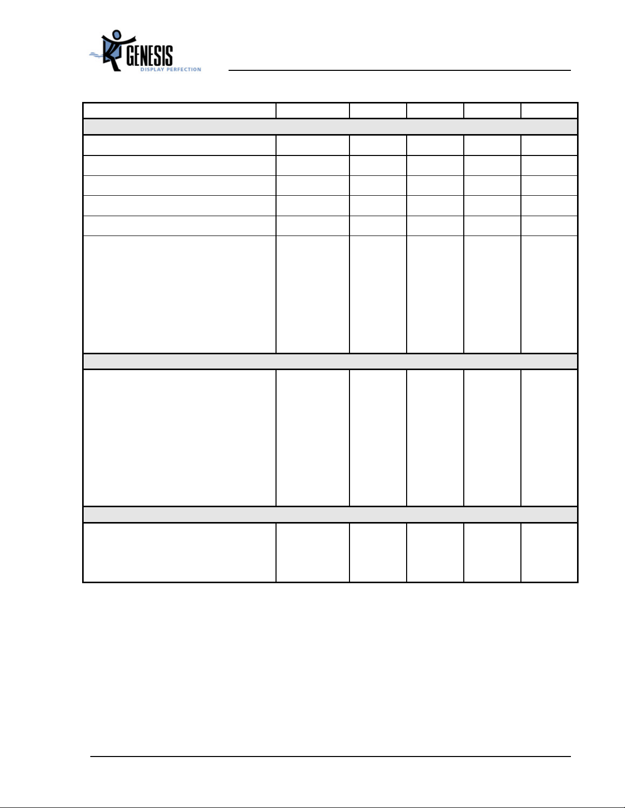
gm2121 Preliminary Data Sheet
Table 20. DC Characteristics
PARAMETER SYMBOL MIN TYP MAX
POWER
(1)
UNITS
Power Consumption @ 135 MHz
Power Consumption @ Low Power Mode
(2)
P
3.3V Supply Voltages V
2.5V Supply Voltages V
Supply Current @ Low Power Mode
(2)
I
Total Supply Current @ CLK =135MHz
• 2.5V digital supply
• 2.5V analog supply
• 3.3V digital supply
• 3.3V analog supply
(3)
(5)
(4)
(6)
P
0.076 W
LP
VDD_3.3
VDD_2.5
28 mA
LP
I
I
2.5V_VDD
I
2.5V_AVDD
I
3.3V_VDD
I
3.3V_AVDD
1.57 1.726 W
3.0 3.3 3.6 V
2.25 2.5 2.75 V
597
412
80
8
97
656
468
80
11
97
mA
mA
mA
mA
mA
INPUTS
High Voltage VIH 2.0 VDD V
Low Voltage VIL GND 0.8 V
Clock High Voltage V
Clock Low Voltage V
2.4 VDD V
IHC
GND 0.4 V
ILC
High Current (VIN = 5.0 V) IIH -25 25 µA
Low Current (VIN = 0.8 V) IIL -25 25 µA
Capacitance (VIN = 2.4 V) CIN 8 pF
OUTPUTS
High Voltage (IOH = 7 mA) VOH 2.4 VDD V
Low Voltage (IOL = -7 mA) VOL GND 0.4 V
Tri-State Leakage Current IOZ -25 25 µA
NOTES:
(1) Maximum current figures are provided for the purposes of selecting an appropriate power supply circuit.
(2) Low power figures result from setting the ADC and clock power down bits so that only the micro-controller is running.
(3) Includes 2.5V digital core (CVDD)
(4) Includes pins VDD1_ADC_2.5, VDD2_ADC_2.5 and LVDS transmitter power pins
(5) Includes pins VDD_DPLL, VDD_SDDS, VDD_DDDS and RVDD.
(6) Includes pins AVDD_ADC, AVDD_RED, AVDD_GREEN, AVDD_BLUE, AVDD_RPLL, AVDD_SDDS, and AVDD_DDDS.
C2121-DAT-01F 47 December 2002
http://www.genesis-microchip.com
Page 48
gm2121 Preliminary Data Sheet
5.2 Preliminary AC Characteristics
The following targeted specifications have been derived by simulation.
All timing is measured to a 1.5V logic-switching threshold. The minimum and maximum operating
T
conditions used were:
= 0 to 125° C, Vdd = 2.35 to 2.65V, Process = best to worst, CL = 16pF for all outputs.
DIE
Table 21.
Clock Domain Max Speed of Operation
Maximum Speed of Operation
Main Input Clock (TCLK) 24 MHz ( 20.0MHz recommended)
ADC Clock (ACLK) 162.5MHz
HCLK Host Interface Clock (6-wire protocol) 5 MHz
Input Format Measurement Clock (IFM_CLK) 50MHz ( 20.0MHz recommended)
Reference Clock (RCLK) 200MHz (200MHz recommended)
On-Chip Microcontroller Clock (OCM_CLK) 100 MHz
Display Clock (DCLK) 135 MHz
Table 22. Display Timing and DCLK Adjustments
DP_TIMING -> Tap 0 (default) Tap 1 Tap 2 Tap 3
Min
(ns)
Max
(ns)
Min
(ns)
Max
(ns)
Min
(ns)
Max
(ns)
Min
(ns)
Max
(ns)
Propagation delay from DCLK to DA*/DB* 1.0 4.5 0.5 3.5 -0.5 2.5 -1.5 1.5
Propagation delay from DCLK to DHS 1.0 4.5 0.5 3.5 -0.5 2.5 -1.5 1.5
Propagation delay from DCLK to DVS 0.5 4.5 0.0 3.5 -1.0 2.5 -2.0 1.5
Propagation delay from DCLK to DEN 1.0 4.5 0.5 3.5 -0.5 2.5 -1.5 1.5
Note: DCLK Clock Adjustments are the amount of additional delay that can be inserted in the DCLK path, in order to reduce the
propagation delay between DCLK and its related signals.
Table 23. 2-Wire Host Interface Port Timing
Parameter Symbol MIN TYP MAX Units
SCL HIGH time T
SCL LOW time T
SDA to SCL Setup T
SDA from SCL Hold T
Propagation delay from SCL to SDA T
Note: The above table assumes OCM_CLK = R_CLK / 2 = 100 MHz (default) (ie 10ns / clock)
1.25 us
SHI
1.25 us
SLO
30 ns
SDIS
20 ns
SDIH
10 150 ns
SDO3
C2121-DAT-01F 48 December 2002
http://www.genesis-microchip.com
Page 49
5.3 External ROM Interface Timing Requirements
TRC
TACC
gm2121 Preliminary Data Sheet
ROM_DATA[7:0]
ROM_ADDR[15:0]
ROM_OEn
MICRO_CLK
(internal)
Latched Data
(internal)
TMICRO_CLK
74 A0
00F4 00F5 00F6
TOE
74 A0
Address Asserted Data Latched
Figure 31. External ROM Interface Timing Diagram
T
MICRO_CLK
MICRO_CLK is the internal MCU clock derived from TCLK and has the same frequency as TCLK. At the maximum
supported TCLK frequency (24MHz) the MICRO_CLK period is about 41ns.
The ROM data is latched on the third MICRO_CLK rising edge after the ADDRESS bus is asserted. Due to this
requirement, the external ROM should have a maximum access time of equal to or less than three TCLK periods (for
example, less than 123 ns when 24MHz TCLK crystal is used).
= 1 / f
= 1 / 24MHz = 41.6 ns (if 24MHz TCLK crystal is used)
TCLK
There are three criteria to be met for the external ROM interface timing (again, using 24MHz TCLK as a worst-case
example):
1. T
2. T
3. T
= 4 x T
RC
ACCmax
≤ 2 x T
OE
MIRCO_CLK
≤ 3 x T
MIRCO_CLK
= 166.4 ns
MIRCO_CLK
= 83.2 ns
= 124.8 ns
C2121-DAT-01F 49 December 2002
http://www.genesis-microchip.com
Page 50
gm2121 Preliminary Data Sheet
6 Ordering Information
Order Code
Application Package Temperature
Range
gm2121 SXGA 160-pin PQFP 0-70°C
C2121-DAT-01F 50 December 2002
http://www.genesis-microchip.com
Page 51
gm2121 Preliminary Data Sheet
7 Mechanical Specifications
A
B
121
160
pin 1 40
Depressed dot on package indicates pin 1 (lower left corner)
D
80
Symbol Millimeter
Inch
Min Nom Max Min Nom Max
A 30.95 31.20 31.45 1.218 1.228 1.238
B 27.90 28.00 28.10 1.098 1.102 1.106
C 0.65 0.026
C
D 4.25 0.167
E 1.60 0.063
G 3.17 3.32 3.47 0.125 0.131 0.137
H 0.73 0.88 1.03 0.025 0.031 0.037
I 0.05 0.25 0.50 0.002 0.010 0.020
J 0 7 0 7
L 0.22 0.30 0.38 0.008 0.012 0.016
M 0.11 0.15 0.23 0.004 0.006 0.008
E
G
I
HML
J
Figure 32. gm2121 160-pin PQFP Mechanical Drawing
C2121-DAT-01F 51 December 2002
http://www.genesis-microchip.com
 Loading...