

Page 1
G-LINK
RAS
CAS
RAS
512K X 8 CMOS DYNAMIC RAM WITH FAST PAGE MODE
Features : Description :
GLT44108
Preliminary Aug 1999 (Rev.2.1)
∗ 524,288 words by 8 bits organization.
∗ Fast access time and cycle time.
∗ Low power dissipation.
Operating Current-150mA max.
TTL Standby Current-2mA max.
∗ Read-Modify-Write,
-Before-
Refresh, Hidden
-Only Refresh,
Refresh and Test Mode Capability.
∗ 1024 refresh cycles/16ms.
∗ Available in 28pin 400 mil SOJ
∗ Single +5.0V±10% Power Supply.
∗ All inputs and Outputs are TTL-
compatible.
∗ Fast Page Mode supports sustained data
rates up to 50MHZ.
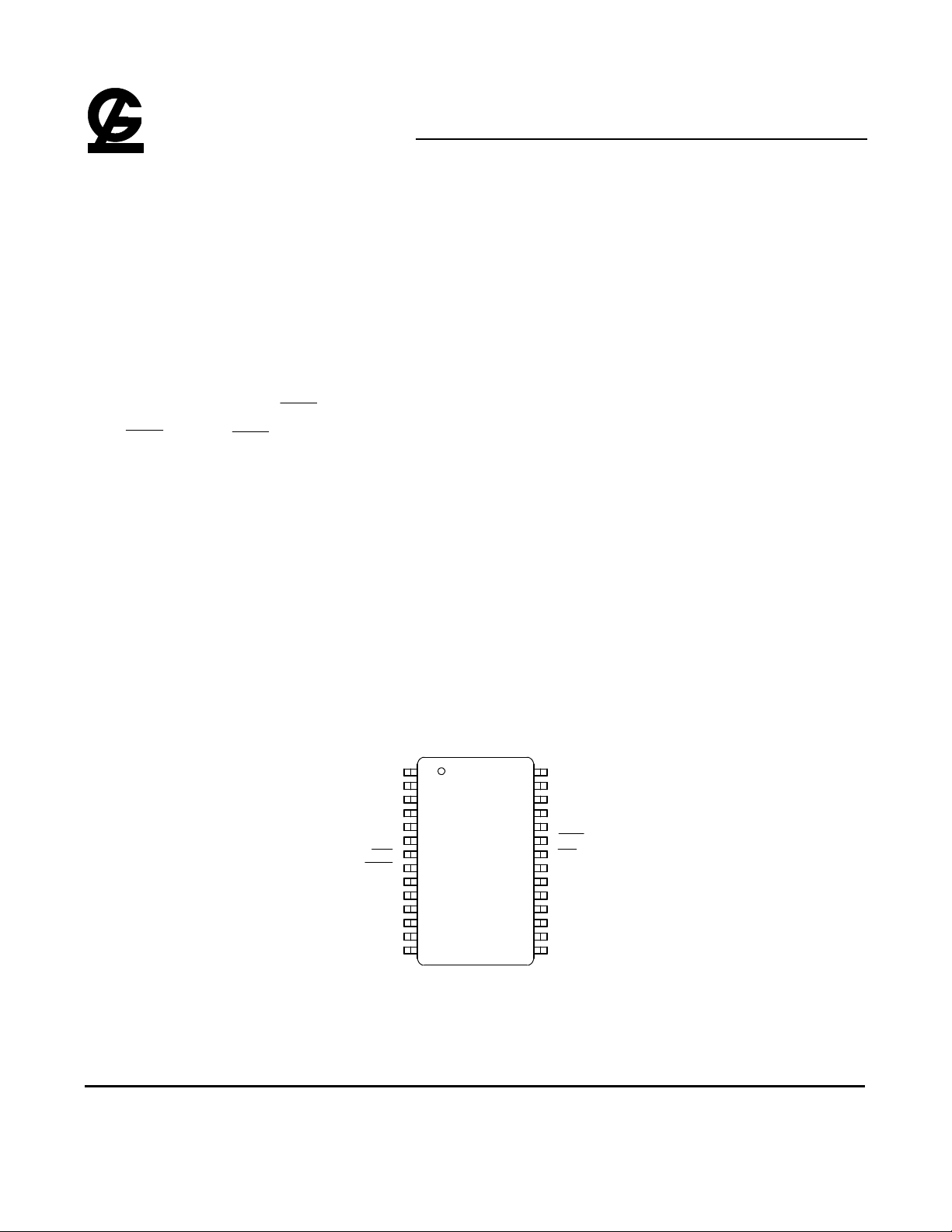
PIN CONFIGURATION :
The GLT44108 is a 524,288 x 8 bit highperformance CMOS dynamic random access
memory. The GLT44108 offers Fast Page mode with
asymmetric address and accepts 512-cycle refresh in
8ms interval.
All inputs are TTL compatible. Fast Page Mode
operation allows random access up to 512 x 8 bits
within a page, with cycle times as short as 22ns.
The GLT44108 is best suited for graphics, digital
signal processing and high performance peripherals.
GLT44108
28 Lead SOJ
G-Link Technology
2701 Northwestern Parkway
Santa Clara, CA 95051, U.S.A.
Vcc
DQ0
DQ1
DQ2
DQ3
NC
WE
RAS
A9
A0
A1
A2
A3
VCC
1
2
3
4
5
6
7
8
9
10
11
12
13
- 1 -
28
27
26
25
24
23
22
21
20
19
18
17
16
15
VSS
DQ
7
DQ6
DQ5
DQ4
CAS
OE
NC
A8
A7
A6
A5
A
4
VSS14
G-Link Technology Corporation,Taiwan
6F, No.24-2, Industry E. RD. IV, Science Based
Industrial Park, Hsin Chu, Taiwan.
Page 2
G-LINK
RAS
CAS
RAS
CAS
WE
OE
.
I/O0
I/O1
I/O2
I/O3
I/O4
I/O5
I/O6
I/O7
GLT44108
512K X 8 CMOS DYNAMIC RAM WITH FAST PAGE MODE
Preliminary Aug 1999 (Rev.2.1)
HIGH PERFORMANCE -40 -50 -60
Max.
Access Time, (t
RAC
)
40 ns 50 ns 60 ns
Max. Column Address Access Time, (tAA) 20 ns 25 ns 30 ns
Min. Fast Page Mode Cycle Time, (tPC) 22 ns 31 ns 40 ns
Min. Read/Write Cycle Time, (tRC) 75 ns 90 ns 110 ns
Max.
Access Time (t
CAC
)
12 ns 13 ns 15 ns
Pin Descriptions:
Name Function
A0 – A
9
Address Inputs
Row Address Strobe
Column Address Strobe
Write Enable
Output Enable
DQ0 - DQ
V
CC
V
SS
7
Data Inputs / Outputs
+5V Power Supply
Ground
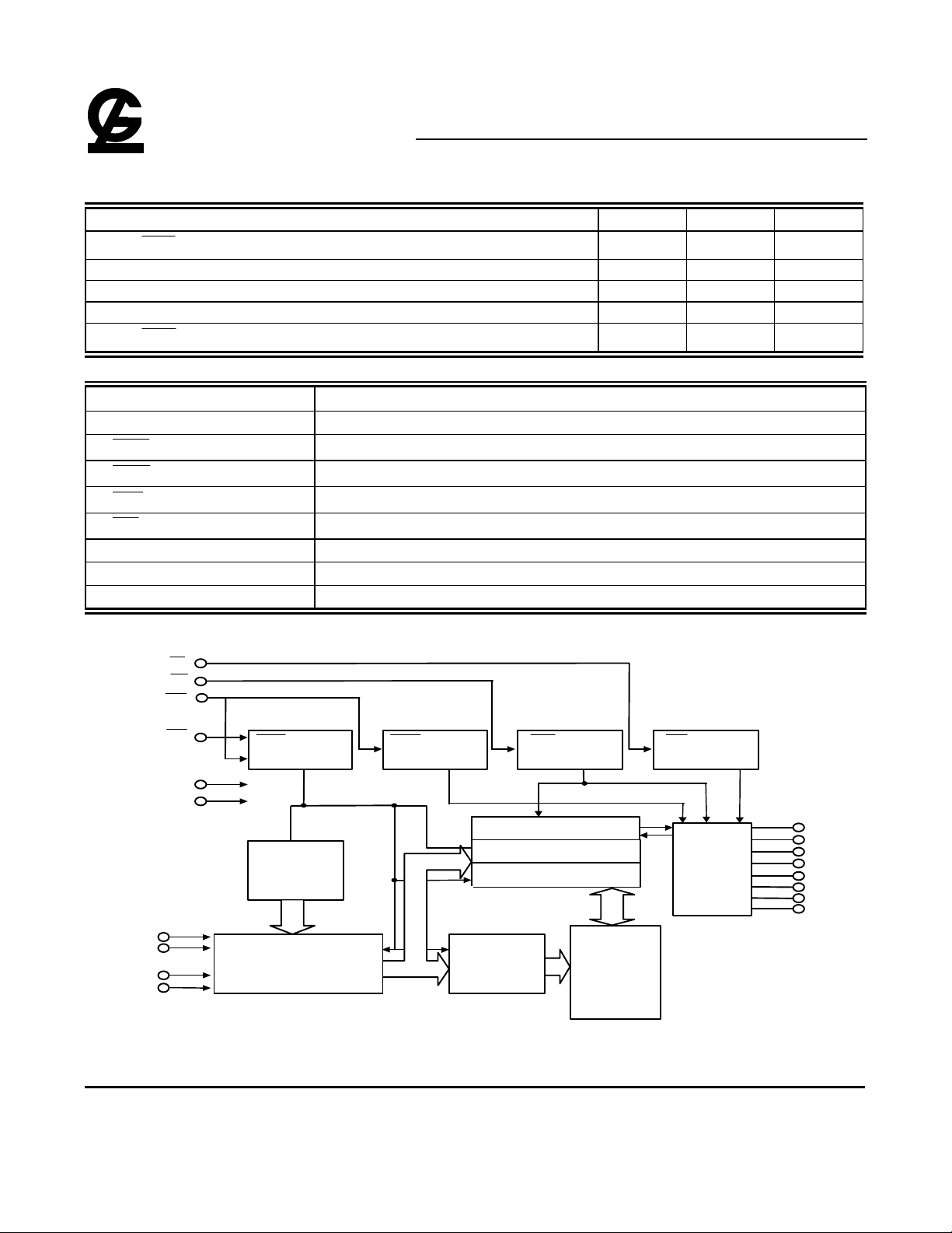
Block Diagram:
OE
WE
CAS
RAS
V
CC
V
SS
A
0
A
1
.
A
8
A
9
RAS
CLOCK
GENERATOR
REFRESH
COUNTER
9
ADDRESS BUFFERS
AND PREDECODERS
CAS
CLOCK
GENERATOR
Y0 - Y
8
DECODERS
X0 - x
9
WE
CLOCK
GENERATOR
Data I/O BUS
COLUMN DECODERS
SENSE AMPLIFIERS
1024
ROW
MEMORY
ARRAY
OE
GENERATOR
512×8
CLOCK
I/O
BUFFER
G-Link Technology
2701 Northwestern Parkway
Santa Clara, CA 95051, U.S.A.
G-Link Technology Corporation,Taiwan
6F, No.24-2, Industry E. RD. IV, Science Based
Industrial Park, Hsin Chu, Taiwan.
- 2 -
Page 3
G-LINK
RAS
CAS
WE ,OE
CAS
RAS
RAS
512K X 8 CMOS DYNAMIC RAM WITH FAST PAGE MODE
Absolute Maximum Ratings* Capacitance*
TA=25°C, VCC=5V±10%, VSS=0V
GLT44108
Preliminary Aug 1999 (Rev.2.1)
Operating Temperature, TA (ambient)
Symbol
......................................-10°C to +80°C
C
Storage Temperature(plastic)....-55°C to +150°C
Voltage Relative to VSS...............-1.0V to + 7.0V
IN1
C
IN2
Short Circuit Output Current......................50mA
C
Power Dissipation......................................1.0W
*Note:Operation above Absolute Maximum Ratings can
adversely affect device reliability.
OUT
*Note: Capacitance is sampled and not 100% tested
Electrical Specifications
l All voltages are referenced to GND.
l After power up, wait more than 200µs and then, execute eight
refresh cycles as dummy cycles to initialize internal circuit.
Parameter
Address Input
,
,
Data Input/Output
before
or
Max.
5
7
7
Unit
pF
pF
pF
only
G-Link Technology
2701 Northwestern Parkway
Santa Clara, CA 95051, U.S.A.
G-Link Technology Corporation,Taiwan
6F, No.24-2, Industry E. RD. IV, Science Based
Industrial Park, Hsin Chu, Taiwan.
- 3 -
Page 4
G-LINK
RAC
RAC
RAC
RAS
CAS
RAS
RAS
CAS
RAC
RAC
RAC
RAS
CAS
RAC
RAC
RAC
CAS
RAS
RAS
CAS
RAC
RAC
RAC
RAS
CAS
512K X 8 CMOS DYNAMIC RAM WITH FAST PAGE MODE
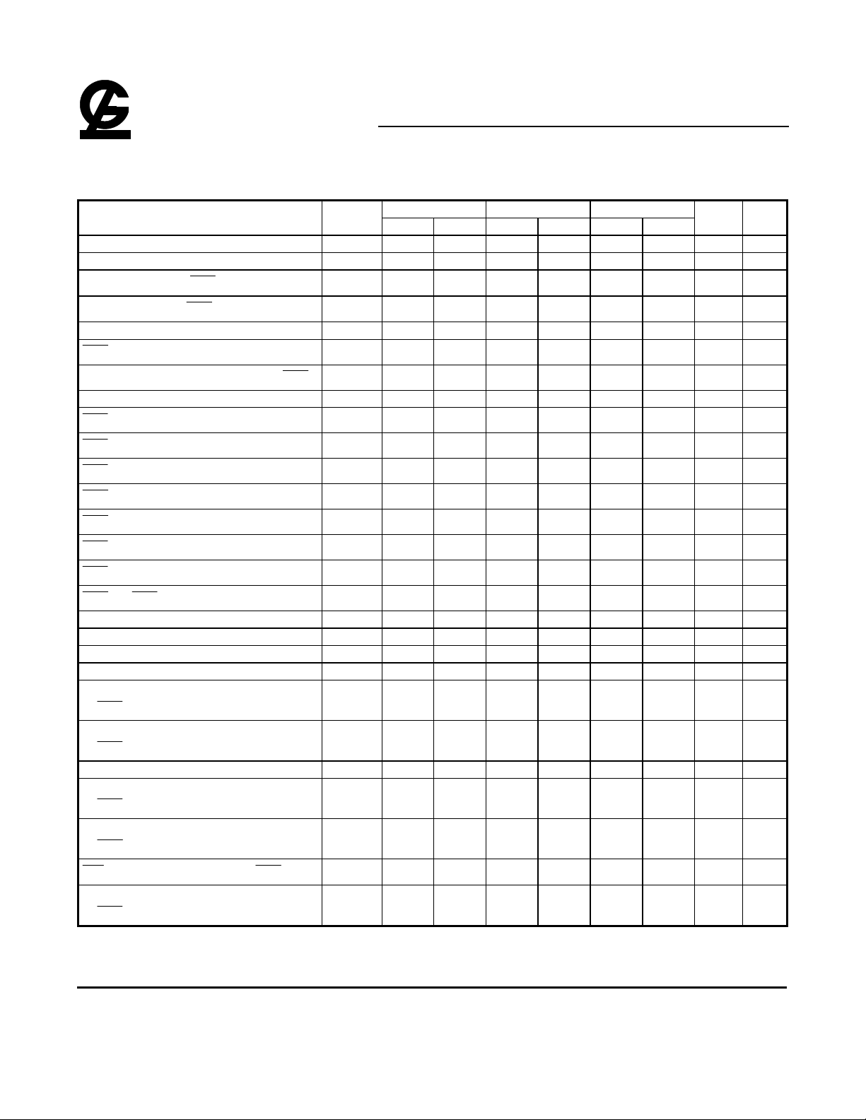
DC and Operating Characteristics (1-2)
TA = 0°C to 70°C, VCC=5V±10%, VSS=0V, unless otherwise specified.
GLT44108
Preliminary Aug 1999 (Rev.2.1)
Sym. Parameter Test Conditions Access
Min. Typ Max. Unit Notes
Time
I
I
I
I
I
I
I
I
V
V
V
V
Notes:
1.ICC is dependent on output loading when the device output is selected. Specified I
2.ICC is dependent upon the number of address transitions specified. I
3. Specified V
Input Leakage Current
LI
(any input pin)
0V ≤ VIN ≤ 5.5V
(All other pins not under
-10 +10
test=0V)
Output Leakage Current
LO
(for High-Z State)
Operating Current,
CC1
0V ≤ V
Output is disabled (Hiz)
Random READ/WRITE tRC = tRC (min.)
Standby Current,(TTL)
CC2
other inputs ≥ V
Refresh Current,
CC3
-Only
≤ 5.5V
out
,
cycling,
at V
IH
, at V
SS
t
= 40ns
t
= 50ns
t
= 60ns
IH
t
= 40ns
t
= 50ns
t
= 60ns
-10 +10
tRC = tRC (min.)
Operating Current,
CC4
FAST Page Mode
Refresh Current,
CC5
Before
Standby Current, (CMOS)
CC6
at V
,
IL
,address
cycling:tPC=tPC(min.)
,
,
address cycling:
tRC=tRC(min.)
≥ VCC-0.2V,
t
t
t
t
t
t
= 40ns
= 50ns
= 60ns
= 40ns
= 50ns
= 60ns
≥ VCC-0.2V,
All other inputs ≥V
Input Low Voltage -1 +0.8 V 3
IL
Input High Voltage 2.4 VCC+1 V 3
IH
Output Low Voltage IOL = 4.2mA 0.4 V
OL
Output High Voltage IOH = -5mA 2.4 V
OH
open.
per address cycle in random Read/Write and Fast Page Mode.
is steady state operation. During transitions, V
IL(min.)
not to exceed 20ns.All AC parameters are measured with V
SS
IL(min.)
IL(min.)≥Vss
is measured with a maximum of one transition
CC(max.)
may undershoot to -1.0V for a period
and V
IH(max.)≤Vcc
150
140
120
2 mA
150
140
120
150
140
120
150
140
120
1 mA
is measured with the output
CC(max.)
.
µA
µA
mA 1,2
mA 2
mA 1,2
mA 1
G-Link Technology
2701 Northwestern Parkway
Santa Clara, CA 95051, U.S.A.
G-Link Technology Corporation,Taiwan
6F, No.24-2, Industry E. RD. IV, Science Based
Industrial Park, Hsin Chu, Taiwan.
- 4 -
Page 5
G-LINK
RAS
CAS
CAS
CAS
RAS
RAS
RAS
CAS
CAS
RAS
RAS
CAS
RAS
RAS
RAS
RAS
CAS
WE
CAS
RAS
512K X 8 CMOS DYNAMIC RAM WITH FAST PAGE MODE
AC Characteristics (0°°C≤≤TA≤≤70°°C,See note 1,2)
Test condition:VCC=5.0V±10%, VIH/VIL=2.4V/0.8V,VOH/VOL=2.0V/0.8V
Parameter 40 ns 50 ns 60 ns
Symbol MIN. MAX. MIN. MAX. MIN. MAX. Unit Notes
Read/Write Cycle Time t
Read Midify Write Cycle Time t
Access Time from
Access Time from
Access Time from Column Address t
to Output in Low-Z
Output Buffer Turn-off Delay from
Transition Time(Rise and Fall) t
Precharge Time
Pulse Width
Hold Time
Hold Time
Pulse Width
to CAS Delay Time
to Column Address Delay Time
to
Precharge Time
Row Address Setup Time t
Row Address Hold Time t
Column Address Setup Time t
Column Address Hold Time t
Column Address Hold Time Referenced
to
Column Address Lead Time Referenced
to
Read Command Setup Time t
Read Command Hold Time Referenced
to
Read Command Hold Time Referenced
to
Hold Time Referenced to
Write Command Hold Time Referenced
to
RC
RWC
t
RAC
t
CAC
AA
t
CLZ
t
OFF
T
t
RP
t
RAS
t
RSH
t
CSH
t
CAS
t
RCD
t
RAD
t
CRP
ASR
RAH
ASC
CAH
t
AR
t
RAL
RCS
t
RRH
t
RCH
t
WCH
t
WCR
75 - 90 - 110 - ns
120 - 140 - 160 - ns
- 40 - 50 - 60 ns 3,4
- 12 - 13 - 15 ns 3,4
- 20 - 25 - 30 ns 3,4
0 - 0 - 0 - ns 3
0 8
3 50
25 40 10000
12 40 12 10000
16 30
11 22
5 0 -
6 0 6 -
30 -
20 -
0 0 -
0 -
6 -
30 -
Preliminary Aug 1999 (Rev.2.1)
0 10 0 13
3 50 3 50
30 - 40 50 10000 60 10000
13 - 15 50 - 60 13 10000 15 10000
18 37 20 45
13 25 15 30
5 - 5 0 - 0 -
8 - 10 0 - 0 8 - 10 -
40 - 45 -
25 - 30 -
0 - 0 0 - 0 -
0 - 0 -
7 - 10 -
40 - 45 -
GLT44108
ns 7
ns 2
ns
ns
ns
ns
ns
ns 4
ns 4
ns 8
ns
ns
ns
ns
ns
ns
ns
ns 9
ns 9
ns 10
ns 5
G-Link Technology
2701 Northwestern Parkway
Santa Clara, CA 95051, U.S.A.
G-Link Technology Corporation,Taiwan
6F, No.24-2, Industry E. RD. IV, Science Based
Industrial Park, Hsin Chu, Taiwan.
- 5 -
Page 6

G-LINK
WE
WE
RAS
WE
CAS
RAS
WE
RAS
CAS
CAS
CAS
RAS
CAS
CAS
RAS
RAS
CAS
CAS
CAS
CAS
RAS
RAS
CAS
OE
OE
OE
WE
Parameter 40 ns 50 ns 60 ns
Symbol MIN. MAX. MIN. MAX. MIN. MAX. Unit Notes
Pulse Width
Lead Time Referenced to
Lead Time Referenced to
Data-In Setup Time t
Data-In Hold Time t
Data Hold Time Referenced to
Refresh Time(256cycles) t
Setup Time
to WE Delay Time
to WE Delay Time
Column Address to WE Delay Time
Setup Time(
before
Refresh)
Hold Time(
before
Refresh)
to
Precharge Time
Precharge Time(CBR Counter Test
Cycle)
Access Time from
Precharge
Fast Page mode Read/Write Cycle Time t
Fast Page mode Read Modify Write Cycle
Time
Precharge Time(Fast Page mode)
Pulse Width(Fast Page mode)
Hold Time from
Precharge
Access Time from
to Delay Time
Output Buffer Turn-off Delay Time fromOE t
t
t
t
t
t
t
t
t
t
t
t
t
t
t
t
t
t
t
t
GLT44108
512K X 8 CMOS DYNAMIC RAM WITH FAST PAGE MODE
Preliminary Aug 1999 (Rev.2.1)
WP
RWL
CWL
DS
DH
DHR
REF
WCS
RWD
CWD
AWD
CSR
CHR
RPC
CPT
CPA
PC
PRWC
CP
RASP
RHCP
OEA
OED
OEZ
6 13 13 -
0 -
6 33 -
- 8
0 60 28 38 -
5 -
10 -
5 20 -
- 25
30 65 -
7 -
125000
40
25 -
- 10
8 0 8
7 - 10 17 - 15 14 - 15 -
0 - 0 -
7 - 10 40 - 45 -
- 8 - 8
0 - 0 70 - 85 33 - 38 43 - 53 -
5 - 5 -
10 - 10 -
5 - 5 20 - 20 -
- 30 - 35
35 - 40 80 - 90 -
8 - 10 50
125000
60
125000
30 - 35 -
- 13 - 15
10 - 13 -
0 10 0 13
ns 10
ns
ns
ns 11
ns 11
ns 6
ms
ns 5
ns 5
ns 5
ns 5
ns
ns
ns
ns
ns 3
ns
ns
ns
ns
ns
ns
ns
ns 7
Hold Time
Hold Time(Hidden Refresh Cycle)
G-Link Technology
2701 Northwestern Parkway
Santa Clara, CA 95051, U.S.A.
t
OEH
t
WHR
0 -
15 -
0 - 0 15 - 15 -
ns
ns
G-Link Technology Corporation,Taiwan
6F, No.24-2, Industry E. RD. IV, Science Based
Industrial Park, Hsin Chu, Taiwan.
- 6 -
Page 7

Notes
RAS
CAS
RAS
RAS
CAS
CAS
WE
G-LINK
GLT44108
512K X 8 CMOS DYNAMIC RAM WITH FAST PAGE MODE
Preliminary Aug 1999 (Rev.2.1)
1. An initial pause of 200µs is required after power-up followed by any 8
before
2. V
IH(min.)
are measured between V
Refresh cycles to initialize the internal circuit.
and V
are reference levels for measuring timing of input signals. Transition times
IL(min.)
IH(min.)
and V
are assumed to be 5ns for all inputs.
IL(max.)
only Refresh or
3. Measured with an equivalent to 1 TTL loads and 50pF.
4. For read cycles, the access time is defined as follows:
Input Conditions Access Time
t
RAD
t
RAD(max.)
t
RCD(max.)
t
RAD(MAX.)
≤ t
RAD(MAX.)
< t
RAD
< t
RCD
and t
and t
and t
RCD(MAX.)
≤ t
RCD
RCD(MAX.)
≤ t
RCD
RCD(MAX.)
indicate the points which the access time changes and are not the limits of
t
t
t
RAC(MAX.)
AA(MAX.)
CACMAX.)
operation.
5. t
WCS,tRWD,tCWD
as electric characteristics only. If t
will remain high impedance for the duration of the cycle.If t
t
≥ t
AWD
AWD(min.)
and t
are non restrictive operating parameters. They are included in the data sheet
AWD
WCS
≥ t
WCS(min.)
, the cycle is an early write cycle and the data output
CWD
≥ t
CWD(min.),tRWD
≥ t
RWD (min.)
and
, then the cycle is a read-modify-write cycle and the data output will contain the data
read from the selected address. If neither of the above conditions is satisfied, the condition of the
data
out is indeterminate.
6. tAR,t
7. t
OFF(max.)
WCR
, and t
and t
are referenced to t
DHR
OEZ(max.)
define the time at which the output achieves the open circuit condition and are
RAD(max.)
.
not referenced to VOH or VOL.
8. t
CRP(min)
9. Either t
10. t
requirement should be applicable for
WP(min.)
RCH(min.)
or t
RRH(min.)
is applicable for late write cycle or read modify write cycle. In early write cycles,t
must be satisfied for a read cycle.
,
cycle preceded by any cycles.
should be satisfied.
WCH(min.)
11.This specification is referenced to
late write or read modify write cycles.
G-Link Technology
2701 Northwestern Parkway
Santa Clara, CA 95051, U.S.A.
falling edge in early write cycles and to
G-Link Technology Corporation,Taiwan
6F, No.24-2, Industry E. RD. IV, Science Based
Industrial Park, Hsin Chu, Taiwan.
- 7 -
falling edge in
Page 8

G-LINK
t
t
GLT44108
512K X 8 CMOS DYNAMIC RAM WITH FAST PAGE MODE
Preliminary Aug 1999 (Rev.2.1)
Read Cycle
V
IH-
RAS
V
IL-
V
IH-
CAS
V
IL-
V
WE
OE
DQ
IH-
V
IL-
V
IH-
IL-
V
V
IH-
V
IL-
V
OH-
V
OL-
Address
Early Write Cycle NOTE : D
VIH-
RAS
VIL-
tCRP
tASR tRAH
ROW
ADDRESS
= Open
OUT
tRAS
CSH
t
tRCD tRSH
tRAD
tASC
COLUMN
ADDRESS
tRCS
AR
t
tRAC
OPEN
tRAS
tCAH
tAA
tCLZ
tRAL
t
tCAC
RC
OEA
RC
tCAS
tOEZ
DATA-OUT
tRP
tRP
tRRH
tCRP
tRCH
tOFF
Don't Care
VIH-
CAS
VIL-
DQ
WE
OE
VIH-
VIL-
VIH-
VIL-
VIH-
VIL-
VIH-
VIL-
Address
G-Link Technology
2701 Northwestern Parkway
Santa Clara, CA 95051, U.S.A.
tCRP
tASR
tRAH
ROW
ADDRESS
tCSH
tRCD tRSH
tRAD
tASC
COLUMN
ADDRESS
tCAH
tCWL
tAR
tWCR
tWCS
tDHR
tDS tDH
DATA - IN
- 8 -
tCRP
tCAS
tRAL
tRWL
tWCH
tWP
Don't Care
G-Link Technology Corporation,Taiwan
6F, No.24-2, Industry E. RD. IV, Science Based
Industrial Park, Hsin Chu, Taiwan.
Page 9

G-LINK
t
GLT44108
512K X 8 CMOS DYNAMIC RAM WITH FAST PAGE MODE
Preliminary Aug 1999 (Rev.2.1)
Late Write Cycle ( OE Controlled Write) NOTE : D
V
IH-
RAS
V
IL-
t
CAS
Address
WE
OE
CRP
V
IH-
V
IL-
t
ASR
t
V
IH-
V
IL-
V
IH-
V
IL-
V
IH-
V
IL-
RAH
ROW
ADDRESS
t
RAD
t
t
RCS
ASC
t
RCD
t
OED
t
V
IH-
DQ
V
IL-
Read - Modify - Write Cycle
V
IH-
RAS
V
IL-
= Open
OUT
t
RAS
t
CSH
COLUMN
ADDRESS
DS
COLUMN
ADDRESS
t
CAH
t
t
t
DH
RAS
t
OEH
WP
t
t
t
RC
RAL
t
CAS
CWL
t
RSH
t
RWL
RC
t
RP
t
CRP
Don't Care
t
RP
CAS
Address
WE
OE
V
DQ
V
G-Link Technology
2701 Northwestern Parkway
Santa Clara, CA 95051, U.S.A.
V
V
V
V
V
V
V
V
I/OH-
I/OL-
t
t
CRPtRCD
IH-
IL-
t
RAD
t
ASR
t
ASC
t
IH-
IL-
IH-
IL-
IH-
IL-
RAH
ROW
ADDR.
COLUMN
ADDRESS
t
AA
t
RAC
t
CAH
t
OEA
t
CLZ
t
AWD
t
CWD
t
CAC
VALID
DATA-OUT
t
CSH
t
OEZ
t
RSH
t
CAS
t
RWL
t
CWL
t
WP
t
OED
t
DS
t
DH
VALID
DATA-IN
CRP
Don't Care
G-Link Technology Corporation,Taiwan
6F, No.24-2, Industry E. RD. IV, Science Based
Industrial Park, Hsin Chu, Taiwan.
- 9 -
Page 10

G-LINK
t
t
t
GLT44108
512K X 8 CMOS DYNAMIC RAM WITH FAST PAGE MODE
Preliminary Aug 1999 (Rev.2.1)
Fast Page Read Cycle
VIH-
RAS
VIL-
tCRP t
VIH-
CAS
VIL-
tASR
WE
OE
DQ
VIH-
VIL-
VIH-
VIL-
VIH-
VIL-
VIH-
VIL-
ADDR.
Address
Fast Page Write Cycle NOTE : D
VIH-
RAS
IL-
V
tCRP tRCD tCAS
VIH-
CAS
VIL-
tASR
Address
WE
OE
VIH-
VIL-
VIH-
VIL-
VIH-
VIL-
ROW
ADDR.
ROW
OUT
RCDtCAS
tRAD
tRAH
tASC
t
RCS
tRAC
tCLZ
= Open
tRAD
tRAH
tASC
tWCS
tDS tDS tDStDH
t
CP
tCSH
tCAH
COLUMN
ADDRESS
tRCH
tASC
COLUMN
ADDRESS
tRCS tRCS
tCAC
tOEA
tAA
DATA-UOT
VALID
tOFF
tOEZ
tAA
tPC
tCP tCP
tCSH
tCAH
COLUMN
ADDRESS
tASC tASC
COLUMN
ADDRESS
tWCH tWCS tWCStWCH
tWP
tWP tWP
tCWL
RASP
tPC tPC
tCAS
tCAH tCAH
t
CP
tASC
COLUMN
ADDRESS
tAA
tCLZ
RASP
VALID
DATA-UOT
tOEZ
tPC
tCAS
tCAH tCAH
COLUMN
ADDRESS
tCWL tCWL
tDS
tCAC
tOEA
tCLZ
tRHCP
tDS
t
RSH
tCAS
DATA-UOT
tRSH
tCAS
tWCH
tOEZtOFF
VALID
tRWL
tRCH
tOFF
tRP
tRRH
Don't Care
RP
VIH-
DQ
VIL-
G-Link Technology
2701 Northwestern Parkway
Santa Clara, CA 95051, U.S.A.
VALID
DATA-IN
VALID
DATA-IN
VALID
DATA-IN
Don't Care
G-Link Technology Corporation,Taiwan
6F, No.24-2, Industry E. RD. IV, Science Based
Industrial Park, Hsin Chu, Taiwan.
- 10 -
Page 11

G-LINK
t
t
t
t
GLT44108
512K X 8 CMOS DYNAMIC RAM WITH FAST PAGE MODE
Preliminary Aug 1999 (Rev.2.1)
Fast Page Mode Late Write Cycle
VIH-
RAS
IL-
V
tCRP tRCD tCAS
VIH-
CAS
VIL-
tRAD
tASR tRAH
Address
VIH-
VIL-
ROW
ADDR.
tRCS
VIH-
WE
VIL-
VIH-
OE
VIL-
tOED
DQ
VIH-
VIL-
Hi-Z Hi-Z Hi-Z
Fast Page Read - Modify - Write Cycle
IH-
V
RAS
IL-
V
tRCD tCAS tCP tCAS
tRAD
tRAH
tCAH
tASC
ROW
ADDR.
COL.
ADDR.
tRCS
tRWD
tOEA
tCAC
tAA
tRAC
tCLZ tCLZ
CAS
Address
WE
OE
DQ
VIH-
VIL-
tASR
VIH-
VIL-
IH-
V
IL-
V
VIH-
VIL-
I/OH-
V
I/OL-
V
RASP
tCSH
tCP tCP
tCAS
tCAH
tASC
COLUMN
ADDRESS
tCWL tCWL
tWP
tCAH tCAH
tASC tASC
COLUMN
ADDRESS
tRCS tRCS tRWL
tWP
tOEH tOEH tOEH
tDH
tOED
tDH tOED
VALID
DATA-IN
RASP
tDS
DATA-IN
VALID
tDS
tCSH
tASC
COL.
ADDR.
tCWL
WP
tCWD
t
tAWD
tDH
tOED
DS
t
tOEZ
VALID
DATA-OUT
VALID
DATA-IN
tPC
tCAH
tOEA
tCAC
tAA
COLUMN
ADDRESS
tAWD
tCPWD
tRHCP
tWP
tDS
tDH
VALID
DATA-IN
tRSH
tPRWC
tRAL
tCWD
tOED
tOEZ
VALID
DATA-OUT
tCAS
tRAL
tRSH
tCWL
tWP
tOEH
tDH
VALID
DATA-IN
RP
tCRP
Don't Care
RP
tCRP
tRWL
tCWL
tDS
Don't Care
G-Link Technology
2701 Northwestern Parkway
Santa Clara, CA 95051, U.S.A.
G-Link Technology Corporation,Taiwan
6F, No.24-2, Industry E. RD. IV, Science Based
Industrial Park, Hsin Chu, Taiwan.
- 11 -
Page 12

G-LINK
tRCt
tRCt
t
t
GLT44108
512K X 8 CMOS DYNAMIC RAM WITH FAST PAGE MODE
Preliminary Aug 1999 (Rev.2.1)
CAS
Before
RAS
Refresh Cycle
RAS
VIH-
VIL-
tCSR tCSRtCHR tCHRtRPC tRPC tCRP
VIH-
CAS
VIL-
RAS -Only Refresh Cycle
V
IH-
RAS
IL-
V
V
IH-
CAS
V
IL-
V
Address
IH-
V
IL-
Hidden Refresh Cycle ( Read )
V
IH-
RAS
V
IL-
tRAS
RC
RC
tRAS tRAS
tRP
tCRP
tASR
ROW ROW
RC
t
RAS
tRAStRP
tRP
tRP
tRPC tCRP
tASRtRAH
tRAH
t
RP
t
RAS
RC
t
RP
V
IH-
CAS
V
IL-
V
WE
OE
DQ
IH-
V
IL-
V
IH-
V
IL-
V
IH-
V
IL-
V
IH-
V
IL-
Address
G-Link Technology
2701 Northwestern Parkway
Santa Clara, CA 95051, U.S.A.
t
CRP
t
ASRtCAH
ROW
ADDRESS
t
RAD
OPEN
t
t
RCD
RCS
t
t
RAC
ASC
COLUMN
ADDRESS
t
CAH
t
t
RAL
t
AA
t
CLZ
- 12 -
RSH
t
t
CAC
OEA
t
CHR
t
WHR
t
t
OEZ
DATA-OUT
OFF
Don't Care
G-Link Technology Corporation,Taiwan
6F, No.24-2, Industry E. RD. IV, Science Based
Industrial Park, Hsin Chu, Taiwan.
Page 13

G-LINK
t
t
GLT44108
512K X 8 CMOS DYNAMIC RAM WITH FAST PAGE MODE
Preliminary Aug 1999 (Rev.2.1)
Hidden Refresh Cycle ( Write ) NOTE : D
V
IH-
RAS
V
IL-
t
t
RAD
CAS
Address
WE
OE
DQ
t
CRP
V
IH-
V
IL-
t
ASCtCAH
V
IH-
IL-
V
V
IH-
V
IL-
V
IH-
V
IL-
V
IH-
V
IL-
ROW
ADDRESS
RCD
OUT
t
t
WCS
=Open
t
RAS
ASC
COLUMN
ADDRESS
DS
t
t
DATA-IN
CAH
RC
t
RSH
t
WCH
t
WP
DH
t
t
RP
t
CHR
t
RAS
RC
Don't Care
t
RP
G-Link Technology
2701 Northwestern Parkway
Santa Clara, CA 95051, U.S.A.
G-Link Technology Corporation,Taiwan
6F, No.24-2, Industry E. RD. IV, Science Based
Industrial Park, Hsin Chu, Taiwan.
- 13 -
Page 14

G-LINK
GLT44108
512K X 8 CMOS DYNAMIC RAM WITH FAST PAGE MODE
Preliminary Aug 1999 (Rev.2.1)
CAS
- Before
RAS
RAS
CAS
Address
Read Cycle
Write Cycle
Read-Modify-Write
DQ
Refresh Counter Test Cycle
VIH-
VIL-
t
CSR
t
WRPtWRH
t
WRP
t
WRH
WE
OE
DQ
WE
OE
DQ
WE
OE
VIH-
VIL-
V
VIL-
VIH-
VIL-
V
VIL-
VOH-
VOL-
VIH-
VIL-
VIH-
VIL-
VIH-
VIL-
VIH-
VIL-
VIH-
VIL-
VI/OH-
VI/OL-
IH-
IH-
t
CHR
OPEN
t
WCS
t
RAS
t
CPT
t
ADDRESS
t
ASC
COLUMN
t
t
DS
VALID DATA-IN
RCS
CLZ
t
t
t
t
AA
t
CLZ
AA
t
t
CAC
CAC
t
OEA
t
CAH
RCS
t
OEA
t
CWL
t
WCH
t
WP
t
AWD
t
CWD
DATA-OUT
t
RSH
t
CAS
t
RAL
VALID DATA-OUT
t
RWL
DH
t
OED
t
OEZ
VALID
t
t
RWL
t
WP
t
DH
t
DS
VALID
DATA-IN
OEZ
t
CWL
t
RP
t
RRH
t
Don't Care
CEZ
t
RCH
G-Link Technology
2701 Northwestern Parkway
Santa Clara, CA 95051, U.S.A.
G-Link Technology Corporation,Taiwan
6F, No.24-2, Industry E. RD. IV, Science Based
Industrial Park, Hsin Chu, Taiwan.
- 14 -
Page 15

G-LINK
Part Number
SPEED
POWER
FEATURE
PACKAGE
512K X 8 CMOS DYNAMIC RAM WITH FAST PAGE MODE
Ordering Information
GLT44108-40J4 40ns Normal FPM SOJ 400mil 28L
GLT44108-50J4 50ns Normal FPM SOJ 400mil 28L
GLT44108-60J4 60ns Normal FPM SOJ 400mil 28L
Parts Numbers (Top Mark) Definition :
GLT44108
Preliminary Aug 1999 (Rev.2.1)
4 : DRAM
6 : Standard
SRAM
7 : Cache SRAM
8 : Synchronous
Burst SRAM
GLT 4 41 08 - 40 J4
-SRAM
064 : 8K
256 : 256K
512 : 512K
100 : 1M
-DRAM
10 : 1M(C/EDO)*
11 : 1M(C/FPM)*
12 : 1M(H/EDO)*
13 : 1M(H/FPM)*
20 : 2M(EDO)
21 : 2M(FPM)
40 : 4M(EDO)
41 : 4M(FPM)
80 : 8M(EDO)
81 : 8M(FPM)
*See note
CONFIG.
04 : x04
08 : x08
16 : x16
32 : x32
VOLTAGE
Blank : 5V
L : 3.3V
M : Mix Voltage
SPEED
-SRAM
12 : 12ns
15 : 15ns
20 : 20ns
70 : 70ns
-DRAM
35 : 35ns
40 : 40ns
45 : 45ns
50 : 50ns
60 : 60ns
PACKAGE
T : PDIP(300mil)
TS : TSOP(Type I)
TC : TSOP(Type ll)
PL : PLCC
FA : 300mil SOP
FB : 330mil SOP
FC : 445mil SOP
J3 : 300mil SOJ
J4 : 400mil SOJ
P : PDIP(600mil)
Q : PQFP
TQ : TQFP
Note : CÙCDROM , HÙHDD.
Example :
1.GLT710008-15T 1Mbit(128Kx8)15ns 5V SRAM PDIP(300mil)Package type.
2.GLT44016-40J4 4Mbit(256Kx16)40ns 5V DRAM SOJ(400mil)Package type.
G-Link Technology
2701 Northwestern Parkway
Santa Clara, CA 95051, U.S.A.
G-Link Technology Corporation,Taiwan
6F, No.24-2, Industry E. RD. IV, Science Based
Industrial Park, Hsin Chu, Taiwan.
- 15 -
Page 16

G-LINK
512K X 8 CMOS DYNAMIC RAM WITH FAST PAGE MODE
Package Information
400mil 28 Lead Small Outline J-form Package (SOJ)
GLT44108
Preliminary Aug 1999 (Rev.2.1)
G-Link Technology
2701 Northwestern Parkway
Santa Clara, CA 95051, U.S.A.
G-Link Technology Corporation,Taiwan
6F, No.24-2, Industry E. RD. IV, Science Based
Industrial Park, Hsin Chu, Taiwan.
- 16 -
 Loading...