

Datasheet GLT4160M04E-60TC, GLT4160M04E-60J3, GLT4160M04-70TC, GLT4160M04-70J3, GLT4160M04-60TC Datasheet (G-LINK)
...Page 1
G-LINK
GLT4160M04
4M X 4 CMOS DYNAMIC RAM WITH EXTENDED DATA OUTPUT
Jan 2000 (Rev. 1.3)
G-Link Technology
2701 Northwestern Parkway
Santa Clara, CA 95051, U.S.A.
G-Link Technology Corporation,Taiwan
6F, No. 24-2, Industry E. RD. IV, Science Based
Industrial Park, Hsin Chu, Taiwan.
- 1 -
Features : Description :
∗ 4,194,304 words by 4 bits organization.
∗ Fast access time and cycle time
∗ Low power dissipation.
∗ Read-Modify-Write,
RAS
-Only Refresh,
CAS
-Before-
RAS
Refresh, Hidden Refresh.
∗ 2,048 refresh cycles per 32ms.
∗ Available in 300 mil 26(24) SOJ and TSOPII.
∗ 2.5V±0.2V Vcc Power Supply voltage.
∗ All inputs and Outputs are LVTTL
compatible.
∗ Extended Data-Out (EDO) Page access
cycle.
∗ Self-refresh Capability. (S-Version).
The GLT4160M04 is a highperformance CMOS dynamic random access
memory containing 16,777,216 bits
organized in a x4 configuration. The
GLT4160M04 offers page cycle access with
Extended Data Output. The GLT4160M04
has 11 row- and 11 column-addresses, and
accepts 2048-cycle refresh in 32 ms.
The GLT4160M04 provides EDO PAGE
MODE operation which allows for fast data
access within a row-address defined
boundary, up to 2048 x 4 bits with cycle
times as short as 25ns.
HIGH PERFORMANCE 60 70
Max.
RAS
Access Time, (t
RAC
)
60 ns 70 ns
Max. Column Address Access Time, (tAA) 30 ns 35 ns
Min. Extended Data Out Page Mode Cycle Time, (tPC) 25 ns 30 ns
Min. Read/Write Cycle Time, (tRC) 104 ns 124 ns
Max.
CAS
Access Time (t
CAC
)
15 ns 20 ns
Page 2
G-LINK
GLT4160M04
4M X 4 CMOS DYNAMIC RAM WITH EXTENDED DATA OUTPUT
Jan 2000 (Rev. 1.3)
G-Link Technology
2701 Northwestern Parkway
Santa Clara, CA 95051, U.S.A.
G-Link Technology Corporation,Taiwan
6F, No. 24-2, Industry E. RD. IV, Science Based
Industrial Park, Hsin Chu, Taiwan.
- 2 -
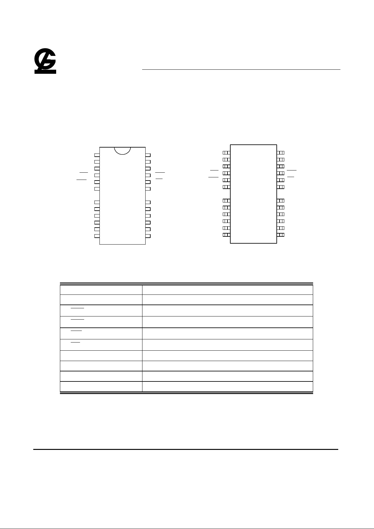
Pin Configuration :
Vcc
DQ0
A
0
A1
A2
A
3
1
2
3
4
5
6
8
9
10
11
12
13
22
21
19
18
17
16
15
14
26
25
24
23
A9
A
8
A7
A6
OE
CAS
VSS
DQ3
DQ1
WE
RAS
NC
VCC
DQ2
A5
A
4
VSS
A
10
Vcc
DQ0
A10
A0
A1
A2
A3
1
2
3
4
5
6
8
9
10
11
12
13
22
21
19
18
17
16
15
14
26
25
24
23
A9
A8
A7
A6
OE
CAS
VSS
DQ3
DQ1
WE
RAS
NC
VCC
DQ2
A5
A4
VSS
Pin Descriptions:
Name Function
A0 - A
10
Address Inputs
RAS
Row Address Strobe
CAS
Column Address Strobe
WE
Write Enable
OE
Output Enable
DQ0 - DQ
3
Data Inputs / Outputs
V
CC
+2.5V Power Supply
V
SS
Ground
NC No Connection
GLT4160M04
300mil 26(24) TSOPII
GLT4160M04
300mil 26(24) SOJ
Page 3
G-LINK
GLT4160M04
4M X 4 CMOS DYNAMIC RAM WITH EXTENDED DATA OUTPUT
Jan 2000 (Rev. 1.3)
G-Link Technology
2701 Northwestern Parkway
Santa Clara, CA 95051, U.S.A.
G-Link Technology Corporation,Taiwan
6F, No. 24-2, Industry E. RD. IV, Science Based
Industrial Park, Hsin Chu, Taiwan.
- 3 -
Absolute Maximum Ratings* Capacitance*
TA=25°C, VCC=2.5V±0.2V, VSS=0V
Operating Temperature, TA (ambient)
.............................................….0°C to
+70°C
For Extended Temperature……………..-20°C to 85°C
Storage Temperature(plastic)............-55°C to +150°C
Voltage Relative to VSS........................-0.5V to + 4.6V
Short Circuit Output Current...............................20mA
Power Dissipation...............................................1.0W
Symbol
C
IN1
C
IN2
C
OUT
Parameter
Address Input
RAS, CAS, WE, OE
Data Input/Output
Max.
5
7
7
Unit
pF
pF
pF
*Note: Operation above Absolute Maximum Ratings can
aversely affect device reliability.
*Note: Capacitance is sampled and not 100% tested
Electrical Specifications
l All voltages are referenced to GND.
l After power up, wait more than 200µs and then, execute eight
CAS
-before-
RAS
or
RAS
-only
refresh cycles as dummy cycles to initialize internal circuit.
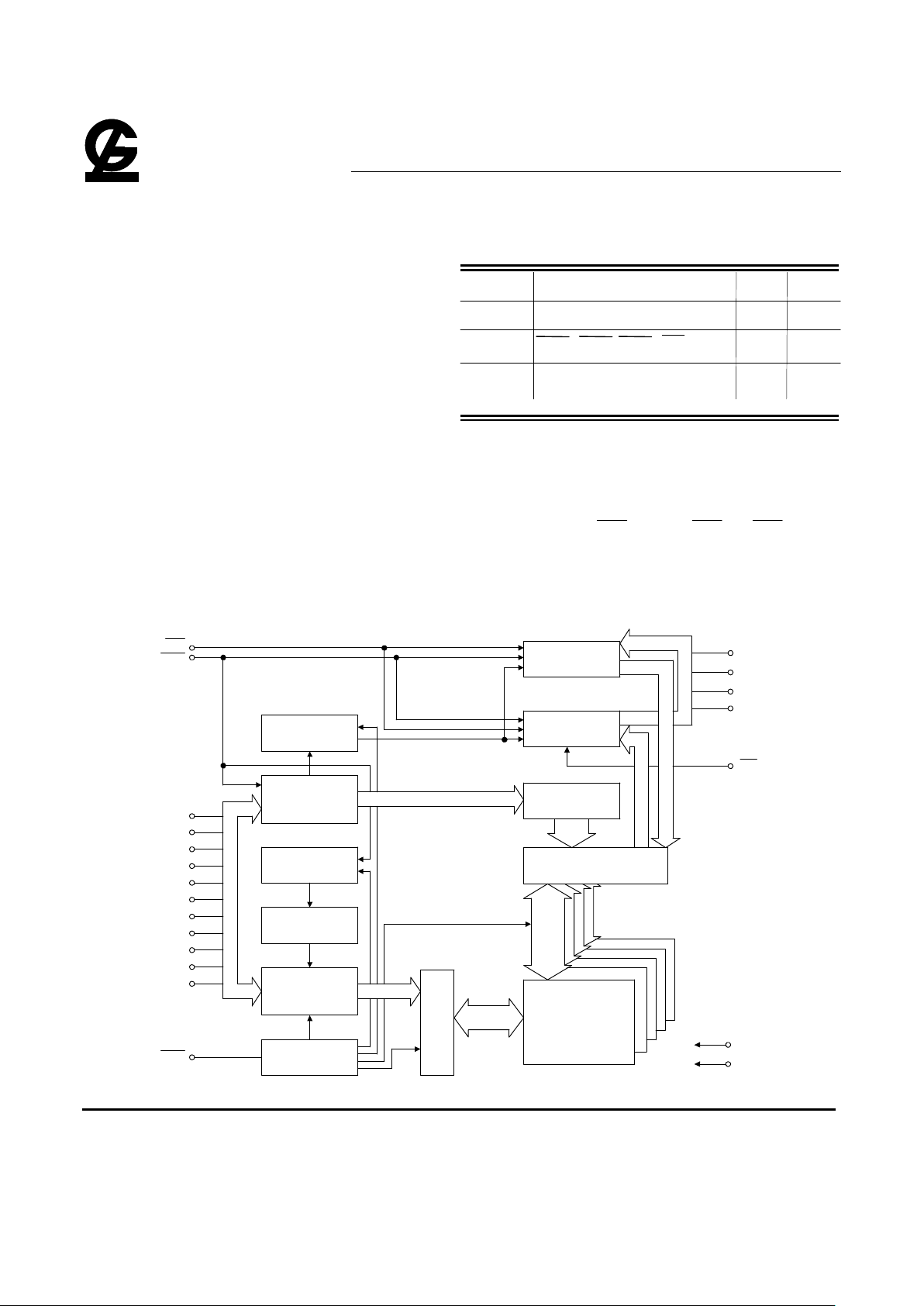
Block Diagram :
NO.2 CLOCK
GENERATOR
COLUMN-
ADDRESS
BUFFER(11)
REFRESH
CONTROLLER
REFRESH
COUNTER
ROW
ADDRESS
BUFFERS(11)
NO.1 CLOCK
GENERATOR
11
11
A1
A2
A3
A4
A5
A6
A7
A8
A9
A10
RAS
11
11
COLUMN
DECODER
DATA-OUT
BUFFER
DATA-IN
BUFFER
SENSE AMPLIFIERS
I/O GATING
2048 x 1024 x 4
MEMORY
ARRAY
2048
2048
4
4
4
4
WE
CAS
DQ0
DQ1
DQ2
DQ3
OE
VDD
VSS
ROW DECODER
2048
A0
Page 4
G-LINK
GLT4160M04
4M X 4 CMOS DYNAMIC RAM WITH EXTENDED DATA OUTPUT
Jan 2000 (Rev. 1.3)
G-Link Technology
2701 Northwestern Parkway
Santa Clara, CA 95051, U.S.A.
G-Link Technology Corporation,Taiwan
6F, No. 24-2, Industry E. RD. IV, Science Based
Industrial Park, Hsin Chu, Taiwan.
- 4 -
Truth Table:
Function
RAS
CAS
WE
OE
ADDRESS DATA-IN/OUT
t
R
t
C
DQ1-DQ4
Standby H
H→X
X X X X High-Z
READ L L H L ROW COL Data-Out
EARLY WRITE L L L X ROW COL Data-In
READ WRITE L L
H→L L→H
ROW COL Data-Out,Data-In
EDO-PAGE-MODE 1st Cycle L
H→L
H L ROW COL Data-Out
READ 2nd cycle L
H→L
H L n/a COL Data-Out
EDO-PAGE-MODE 1st Cycle L
H→L
L X ROW COL Data-In
EARLY-WRITE 2nd cycle L
H→L
L X n/a COL Data-In
EDO-PAGE-MODE 1st Cycle L
H→L H→L L→H
ROW COL Data-Out,Data-In
READ-WRITE 2nd cycle L
H→L H→L L→H
n/a COL Data-Out,Data-In
RAS
-ONLY REFRESH
L H X X ROW n/a High-Z
HIDDEN REFRESH READ
L→H→L
L H L ROW COL Data-Out
WRITE
L→H→L
L L X ROW COL Data-In
CBR REFRESH
H→L
L H X X X High-Z
SELF REFRESH
H→L
L H X X X High-Z
Page 5
G-LINK
GLT4160M04
4M X 4 CMOS DYNAMIC RAM WITH EXTENDED DATA OUTPUT
Jan 2000 (Rev. 1.3)
G-Link Technology
2701 Northwestern Parkway
Santa Clara, CA 95051, U.S.A.
G-Link Technology Corporation,Taiwan
6F, No. 24-2, Industry E. RD. IV, Science Based
Industrial Park, Hsin Chu, Taiwan.
- 5 -
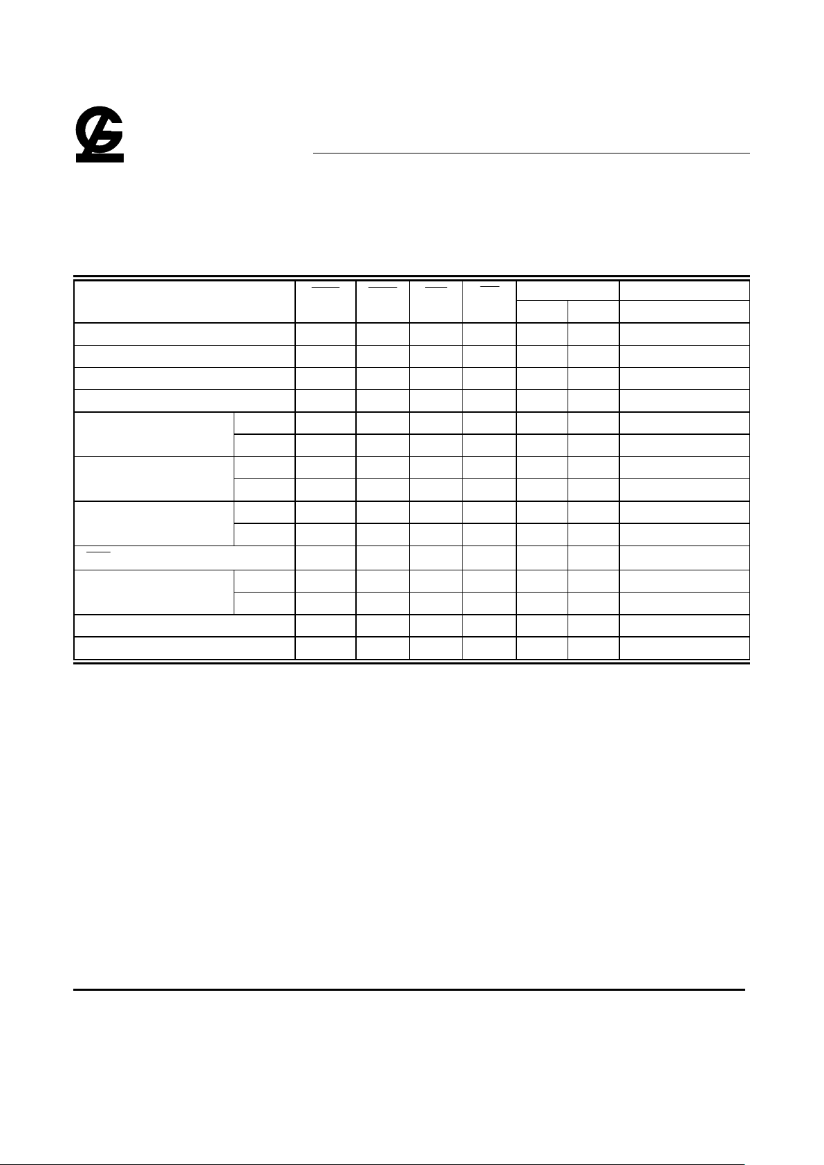
DC and Operating Characteristics (1-2)
TA = 0°C to 70°C, -20°C to 85°C VCC=2.5V±0.2V, VSS=0V, unless otherwise specified.
Sym. Parameter Test Conditions Access
Time
Min. Typ Max. Unit Notes
I
LI
Input Leakage Current
(any input pin)
0V ≤ V
IN
≤ VCC+0.3V
(All other pins not under
test=0V)
-5 +5
µA
I
LO
Output Leakage Current
(for High-Z State)
0V ≤ V
out
≤ V
CC
Output is disabled (Hiz)
-5 +5
µA
I
CC1
Operating Current,
Random READ/WRITE
tRC = tRC (min.) t
RAC
= 60ns
t
RAC
= 70ns
80
70 mA
1,2
I
CC2
Standby Current, (TTL)
RAS, CAS
at V
IH
other inputs ≥V
SS
1 mA
I
CC3
Refresh Current,
RAS
-Only
RAS
cycling,
CAS
at V
IH
tRC = tRC (min.)
t
RAC
= 60ns
t
RAC
= 70ns
80
70 mA
2
I
CC4
Operating Current,
EDO Page Mode
RAS
at VIL,
CAS
address
cycling:tPC=tPC(min.)
t
RAC
= 60ns
t
RAC
= 70ns
80
70 mA
1,2
I
CC5
Refresh Current,
CAS
Before
RAS
RAS, CAS
address
cycling: tRC=tRC (min.)
t
RAC
= 60ns
t
RAC
= 70ns
80
70
mA 1
I
CC6
Standby Current, (CMOS)
RAS
≥VCC-0.2V,
CAS
≥VCC-0.2V,
All other inputs V
SS
200
µA
1
I
CC7
Self refresh Current
RAS=CAS
=0.2V,
WE = OE = A0~A10=VCC-
0.2V or 0.2V
DQ0~DQ3=VCC-0.2V,0.2V
or Open
200
µA
V
IL
Input Low Voltage -0.3 +0.8 V 3
V
IH
Input High Voltage 2.0 VCC+0.3 V 4
V
OL
Output Low Voltage IOL = 2mA 0.4 V
V
OH
Output High Voltage IOH = -2mA 1.8 V
Notes:
1. ICC is dependent on output loading when the device output is selected. Specified ICC(max.) is measured with the output
open.
2. ICC is dependent upon the number of address transitions specified ICC(max.) is measured with a maximum of one
transition per address cycle in random Read/Write and EDO Fast Page Mode.
3. Specified VIL(min.) is steady state operation. During transitions VIL(min.) may undershoot to –0.9V for a period not to
exceed 10ns. All AC parameters are measured with VIL(min.)≥VSS and VIH(max.)≤VCC.
4. Specified VIH(max.) is steady state operation . During transitions VIH(max.) may overshoot to VCC+0.9V for a period not
to exceed 10ns. All AC parameters are measured with VIL(min.) ≥ VSS and VIH(max.) ≤ VCC .
Page 6
G-LINK
GLT4160M04
4M X 4 CMOS DYNAMIC RAM WITH EXTENDED DATA OUTPUT
Jan 2000 (Rev. 1.3)
G-Link Technology
2701 Northwestern Parkway
Santa Clara, CA 95051, U.S.A.
G-Link Technology Corporation,Taiwan
6F, No. 24-2, Industry E. RD. IV, Science Based
Industrial Park, Hsin Chu, Taiwan.
- 6 -
AC Characteristics
TA = 0°C to 70°C , -20°C to 85°C VCC = 2.5 V ± 0.2V, VIH/VIL = 2.0/0.8 V, VOH/VOL = 1.6/0.6V
An initial pause of 200 µs and 8
CAS
-before-
RAS
or
RAS
-only refresh cycles are required after power-up.
60 70
Parameter Symbol Min. Max. Min. Max. Unit Notes
Read or Write Cycle Time
t
RC
104 124 ns
Read Modify Write Cycle Time
t
RWC
140 170 ns
RAS
Precharge Time
t
RP
40 50 ns
RAS
Pulse Width
t
RAS
60 10k 70 10k ns
Access Time from
RAS
t
RAC
60 70 ns 1, 2, 3
Access Time from
CAS
t
CAC
15 20 ns 1, 5, 10
Access Time from Column Address
t
AA
30 35 ns 1, 5, 6
CAS
to Output Low-Z
t
CLZ
3 3 ns
CAS
to Output High-Z
t
CEZ
3 15 3 20 ns
RAS
Hold Time
t
RSH
15 20 ns
CAS
Hold Time
t
CSH
45 50 ns
CAS
Pulse Width
t
CAS
10 10k 15 10k ns
RAS
to
CAS
Delay Time
t
RCD
20 45 20 50 ns
RAS
to Column Address Delay Time
t
RAD
15 30 15 35 ns 7
CAS
to
RAS
Precharge Time
t
CRP
5 5 ns
Row Address Set-Up Time
t
ASR
0 0 ns
Row Address Hold Time
t
RAH
10 10 ns
Column Address Set-Up Time
t
ASC
0 0 ns
Column Address Hold Time
t
CAH
10 15 ns
Column Address to
RAS
Lead Time
t
RAL
30 35 ns
Column Address Hold Time Referenced to
RAS
t
AR
45 50 ns
Read Command Set-Up Time
t
RCS
0 0 ns
Read Command Hold Time Referenced to
CAS
t
RCH
0 0 ns 4
Read Command Hold Time Referenced to
RAS
t
RRH
0 0 ns 4
Write Command Set-Up Time
t
WCS
0 0 ns 8, 9
Write Command Hold Time
t
WCH
10 15 ns
Write Command Pulse Width
t
WP
10 15 ns
Write Command to
RAS
Lead Time
t
RWL
15 30 ns
Write Command to
CAS
Lead Time
t
CWL
10 15
ns
Page 7
G-LINK
GLT4160M04
4M X 4 CMOS DYNAMIC RAM WITH EXTENDED DATA OUTPUT
Jan 2000 (Rev. 1.3)
G-Link Technology
2701 Northwestern Parkway
Santa Clara, CA 95051, U.S.A.
G-Link Technology Corporation,Taiwan
6F, No. 24-2, Industry E. RD. IV, Science Based
Industrial Park, Hsin Chu, Taiwan.
- 7 -
AC Characteristics
60 70
Parameter Symbol Min. Max. Min. Max. Unit Notes
Data Set-Up Time
t
DS
0 0 ns
Data Hold Time
t
DH
10 15 ns
Data Hold Time Referenced to
RAS
t
DHR
45 50 ns
RAS
to WE Delay Time
t
RWD
79 94 ns
CAS
to WE Delay Time
t
CWD
34 44 ns
Column Address to WE Delay Time
t
AWD
49 59 ns
CAS
Precharge to
WE
Delay
t
CPWD
54 64 ns
RAS
to
CAS
Precharge Time
t
RPC
5 5 ns
CAS
precharge time
(
CAS
Before
RAS
counter test cycle)
t
CPT
20 25 ns
Access Time from
CAS
Precharge
t
CPA
35 40 ns
EDO Page Mode Cycle Time
t
PC
25 30 ns
EDO Page Mode Read-Modify-Write Cycle Time
t
PRWC
56 71 ns
CAS
Precharge Time (EDO Page Mode)
t
CP
10 10 ns
RAS
Pulse Width (EDO Page Mode Only)
t
RASP
60 100k 70 100k ns
RAS
Hold Time from
CAS
precharge
t
RHCP
35 40 ns
Access Time from
OE
t
OEA
15 0 20 ns 8
OE
to Data Delay Time
t
OED
15 20 ns
OE
to Output Low-Z
t
OLZ
0 0 ns
OE
to Output High-Z
t
OEZ
3 15 3 20 ns
WE
to Data Delay
t
WED
15 20 ns
OE
Command Hold Time
t
OEH
15 20 ns
Data Output Hold after
CAS
low
t
DOH
5 5 ns
RAS
to Output High-Z
t
REZ
3 15 3 20 ns
WE
to Output High-Z
t
WEZ
3 15 3 20 ns
OE
to
CAS
Hold Time
t
OCH
5 5 ns
CAS
Hold Time to
OE
t
CHO
5 5 ns
OE
Precharge Time
t
OEP
5 5 ns
WE
Puts width (EDO mixed read write cycle)
t
WPE
5 5 ns
CAS
Set-Up Time for
CAS
-before-
RAS
Cycle
t
CSR
5 5 ns
Page 8

G-LINK
GLT4160M04
4M X 4 CMOS DYNAMIC RAM WITH EXTENDED DATA OUTPUT
Jan 2000 (Rev. 1.3)
G-Link Technology
2701 Northwestern Parkway
Santa Clara, CA 95051, U.S.A.
G-Link Technology Corporation,Taiwan
6F, No. 24-2, Industry E. RD. IV, Science Based
Industrial Park, Hsin Chu, Taiwan.
- 8 -
60 70
Parameter Symbol Min. Max. Min. Max. Unit Notes
CAS
Hold Time for
CAS
-before-
RAS
Cycle
t
CHR
10 15 ns
WE
to
RAS
precharge time (
CAS
Before
RAS
refresh )
t
WRP
10 10 ns
WE
to
RAS
hold time (
CAS
Before
RAS
refresh
)
t
WRH
10 10 ns
Transition Time
t
T
2 50 2 50 ns
Refresh Period (2,048 cycles)
t
REF
32 32 ms
Refresh Period (S-Version)
t
REFS
128 128 ms
RAS
Pulse Width (
CAS
Before
RAS
Self
refresh
)
t
RASS
100 100
µs
RAS
precharge Time (
CAS
Before
RAS
Self
refresh
)
t
RPS
110 130 ns
CAS
Hold Time (
CAS
Before
RAS
Self
refresh
)
t
CHS
-50 -50 ns
Page 9

G-LINK
GLT4160M04
4M X 4 CMOS DYNAMIC RAM WITH EXTENDED DATA OUTPUT
Jan 2000 (Rev. 1.3)
G-Link Technology
2701 Northwestern Parkway
Santa Clara, CA 95051, U.S.A.
G-Link Technology Corporation,Taiwan
6F, No. 24-2, Industry E. RD. IV, Science Based
Industrial Park, Hsin Chu, Taiwan.
- 9 -
TEST MODE CYCLE
60 70
Parameter Symbol Min. Max. Min. Max. Unit Notes
Random read or write cycle time
t
RC
109 129 ns
Read-modify-write cycle time
t
RWC
145 175 ns
Access time from
RAS
t
RAC
65 75 ns 1,2,3,7
Access time from
CAS
t
CAC
20 25 ns 1,3,7
Access time from column address
t
AA
35 40 ns 1,2,7
RAS
pulse width
t
RAS
65 10k 75 10k ns
CAS
pulse width
t
CAS
15 10k 20 10k ns
RAS
hold time
t
RSH
20 25 ns
CAS
hold time
t
CSH
50 55 ns
Column address to
RAS
lead time
t
RAL
35 40 ns
CAS
to WE delay time
t
CWD
39 49 ns 8
RAS
to WE delay time
t
RWD
84 99 ns 8
Column address to WE delay time t
AWD
54 64 ns 8
CAS
Precharge to WE delay time
t
CPWD
59 69 ns 8
EDO Page Mode cycle time
t
PC
30 35 ns
EDO page mode read-modify-write cycle time
t
PRWC
61 76 ns
RAS
Pulse width (EDO page cycle)
t
RASP
65 100k 75 100k ns
Access time form
CAS
precharge
t
CPA
40 45 ns 1
OE
access time
t
OEA
20 25 ns
OE
to data delay
t
OED
20 25 ns
OE
command hold time
t
OEH
20 25 ns
Write command set-up time (Test mode in)
t
WTS
10 10 ns
Write command hold time (Test mode in)
t
WTH
10 10 ns
Page 10

G-LINK
GLT4160M04
4M X 4 CMOS DYNAMIC RAM WITH EXTENDED DATA OUTPUT
Jan 2000 (Rev. 1.3)
G-Link Technology
2701 Northwestern Parkway
Santa Clara, CA 95051, U.S.A.
G-Link Technology Corporation,Taiwan
6F, No. 24-2, Industry E. RD. IV, Science Based
Industrial Park, Hsin Chu, Taiwan.
- 10 -
Notes:
1. Measure with a load equivalent to one TTL input and 100 pF.
2. Assumes that t
RCD
≤ t
RCD
(max.). If t
RCD
is greater than t
RCD
(max.), access time will be t
AA
dominant.
3. Assumes that t
RAD
≤ t
RAD
(max.). If t
RAD
is greater than t
RCD
(max.), access time will be
controlled by t
CAC
.
4. Either t
RRH
or t
RCH
must be satisfied for a Read Cycle.
5. Access time is determined by the longest of tAA, t
CAC
and t
CPA
.
6. Assumes that t
RAD
≥ t
RAD
(max.).
7. Operation within the t
RAD
(max.) limit ensures that t
RAC
(max.) can be met. t
RAD
(max.)
is specified as a reference point only. If t
RAD
is greater than the specified t
RAD
(max.)
limit, the access time is controlled by t
CAA
and t
CAC
.
8. t
WCS
, t
RWD
, t
AWD
and t
CWD
are not restrictive operating parameters.
9. t
WCS
(min.) must be satisfied in an Early Write Cycle.
10. tDS and tDH are referenced to the latter occurrence of
CAS
or
WE
.
11. tT is measured between VIH (min.) and VIL (max.). AC-measurements assume tT = 2 ns.
Page 11

G-LINK
GLT4160M04
4M X 4 CMOS DYNAMIC RAM WITH EXTENDED DATA OUTPUT
Jan 2000 (Rev. 1.3)
G-Link Technology
2701 Northwestern Parkway
Santa Clara, CA 95051, U.S.A.
G-Link Technology Corporation,Taiwan
6F, No. 24-2, Industry E. RD. IV, Science Based
Industrial Park, Hsin Chu, Taiwan.
- 11 -
Read Cycle
ROW
ADDRESS
COLUMN
ADDRESS
DATA-OUT
tRC
tRAS
tRP
tCRP
t
CSH
tRCD tRSH
tCAS
tCRP
tASR tRAH
tRAD
tASC
tCAH
tRAL
tRCH
tRRH
tAR
tRCS
t
AA
tOEA
tCEZ
tOEZ
tCAC
tCLZ
tRAC
Don't Care
VIH-
VIL-
RAS
VIH-
V
IL-
CAS
VIH-
VIL-
Address
V
IH-
VIL-
WE
VIH-
VIL-
OE
VOH-
VOL-
DQ
Early Write Cycle NOTE : D
OUT
= OPEN
tRP
tRC
tCRP
tCSH
tCRP
tRCD
tRSH
tCAS
tASR
tRAH
tRAD
tASC
tCAH
tRAL
tCWL
tRWL
tWCR
tWCH
tWP
tWCS
tAR
tDS tDH
tDHR
DATA - IN
COLUMN
ADDRESS
ROW
ADDRESS
VIH-
VIL-
RAS
VIH-
VIL-
CAS
VIH-
VIL-
Address
VIH-
VIL-
WE
VIH-
VIL-
OE
VIH-
VIL-
DQ
Don't Care
tRAS
Page 12

G-LINK
GLT4160M04
4M X 4 CMOS DYNAMIC RAM WITH EXTENDED DATA OUTPUT
Jan 2000 (Rev. 1.3)
G-Link Technology
2701 Northwestern Parkway
Santa Clara, CA 95051, U.S.A.
G-Link Technology Corporation,Taiwan
6F, No. 24-2, Industry E. RD. IV, Science Based
Industrial Park, Hsin Chu, Taiwan.
- 12 -
OE Controlled Write Cycle NOTE : D
OUT
= OPEN
t
RP
t
RC
t
CRP
t
CSH
t
CRP
t
RCD
t
RSH
t
CAS
t
ASR
t
RAH
t
RAD
t
ASC
t
CAH
t
RAL
DATA - IN
COLUMN
ADDRESS
ROW
ADDRESS
V
IH-
V
IL-
RAS
V
IH-
V
IL-
CAS
V
IH-
V
IL-
Address
V
IH-
V
IL-
WE
V
IH-
V
IL-
OE
V
IH-
V
IL-
DQ
Don't Care
t
RAS
t
RCS
t
CWL
t
RWL
t
WP
t
DS
t
OED
t
OEH
t
DH
Read - Modify - Write Cycle
t
RP
t
RC
t
CRP
t
CRPtRCD
t
RSH
VALID
DATA-OUT
COLUMN
ADDRESS
ROW
ADDR.
V
IH-
V
IL-
RAS
V
IH-
V
IL-
CAS
V
IH-
V
IL-
Address
V
IH-
V
IL-
WE
V
IH-
V
IL-
OE
V
I/OH-
V
I/OL-
DQ
Don't Care
t
RAS
VALID
DATA-IN
t
CAS
t
ASR
t
RAH
t
RAD
t
ASC
t
CAH
t
CSH
t
AWD
t
CWD
t
RWL
t
CWL
t
WP
t
OEA
t
CLZ
t
CAC
t
AA
t
RAC
t
DH
t
DS
t
OED
t
OEZ
Page 13

G-LINK
GLT4160M04
4M X 4 CMOS DYNAMIC RAM WITH EXTENDED DATA OUTPUT
Jan 2000 (Rev. 1.3)
G-Link Technology
2701 Northwestern Parkway
Santa Clara, CA 95051, U.S.A.
G-Link Technology Corporation,Taiwan
6F, No. 24-2, Industry E. RD. IV, Science Based
Industrial Park, Hsin Chu, Taiwan.
- 13 -
EDO Page Mode Read Cycle NOTE : D
OUT
= OPEN
tRASP tRP
tCRP
tRCD tCAS
tCSH
tCP
tCAS
tCAS tCAS
tCP tCP
tPC tPC tPC
tCSR
tRAH
tRAD
tASC
tASC
tASC
tASC
tCAH
tCAH
tCAH
tCAH
tRCS
tRCH
tRRH
tOEA
tOEA
tCAC
tCPA
tAA
tOCH
tCPA
tAA
tCAC
tOEP
tCHO
tAA
tCAC
tCPA
tCLZ
tOLZ
tRAC
tCAC
tDOH
tOEZ
tOEP
tOEZ tOEZ
VALID
DATA-OUT
VALID
DATA-OUT
VALID
DATA-OUT
VALID
DATA-OUT
VALID
DATA-OUT
VIH-
VIL-
RAS
VIH-
VIL-
CAS
VIH-
VIL-
Address
VIH-
VIL-
WE
VIH-
VIL-
OE
DQ
VOH-
VOL-
ROW
ADDR.
COLUMN
ADDRESS
COLUMN
ADDRESS
COL.
ADDR.
COL.
ADDR.
Don't Care
tRHCP
EDO Page Mode Early Write Cycle NOTE : D
OUT
= OPEN
tRASP tRP
tCRP
tRCD tCAS
VIH-
VIL-
RAS
VIH-
VIL-
CAS
tCAS
tCAS
tCP tCP
tPC tPC
tRSH
tASR
tRAD
tRAH
tASC
tCAH
tCSH
tASC tASC
tCAH tCAH
tWCS
tWP
tWCH tWCS tWCStWCH
tWCH
tWP tWP
tDS tDS tDStDH
tDS
tDS
VIH-
VIL-
Address
VIH-
VIL-
WE
VIH-
VIL-
OE
DQ
VIH-
VIL-
ROW
ADDR.
COLUMN
ADDRESS
COLUMN
ADDRESS
COLUMN
ADDRESS
VALID
DATA-IN
VALID
DATA-IN
VALID
DATA-IN
Don't Care
tRHCP
Page 14

G-LINK
GLT4160M04
4M X 4 CMOS DYNAMIC RAM WITH EXTENDED DATA OUTPUT
Jan 2000 (Rev. 1.3)
G-Link Technology
2701 Northwestern Parkway
Santa Clara, CA 95051, U.S.A.
G-Link Technology Corporation,Taiwan
6F, No. 24-2, Industry E. RD. IV, Science Based
Industrial Park, Hsin Chu, Taiwan.
- 14 -
EDO Page Mode Read - Modify - Write Cycle NOTE : D
OUT
= OPEN
t
RASP
t
RP
V
IH-
V
IL-
RAS
V
IH-
V
IL-
CAS
Don't Care
t
CSH
t
RCD
t
CAS
t
CP
t
CAS
t
RSH
t
CRP
t
RAD
t
RAH
t
ASR
t
ASC
t
CAH
t
ASC
t
CAH
t
RAL
t
PRWC
t
RCS
t
WP
t
CWL
t
WP
t
CWL
t
RWL
t
CWD
t
AWD
t
RWD
t
OEA
t
CWD
t
AWD
t
CPWD
t
OEA
t
OEH
t
RAC
t
AA
t
CAC
t
OEZ
t
OED
t
DS
t
DH
t
AA
t
CAC
t
OEZ
t
OED
t
DS
t
DH
t
CLZ
t
CLZ
VALID
DATA-OUT
VALID
DATA-IN
VALID
DATA-OUT
VALID
DATA-IN
ROW
ADDR.
COL.
ADDR.
COL.
ADDR.
V
IH-
V
IL-
Address
V
IH-
V
IL-
WE
V
IH-
V
IL-
OE
V
I/OH-
V
I/OL-
DQ
EDO Page Read And Write Mixed Ccycle
t
RASP
t
RP
t
CAS
t
HPC
t
CAS
t
CAS
t
CP
t
CP
t
CP
t
ASR
t
HPC
t
HPC
t
RAH
t
ASC
t
CAH
t
ASC
t
ASC
t
ASC
t
CAH
t
CAH
t
CAH
t
RCS
t
RCH
t
RCS
t
RCH
t
RCH
t
WCStWCH
t
WPE
t
CPA
t
CLZ
t
WED
t
WEZ
t
RAC
t
AA
t
CAC
t
OEA
t
WEZ
t
DS
t
DH
t
AA
t
REZ
VALID
DATA-OUT
VALID
DATA-OUT
VALID
DATA-OUT
VALID
DATA-IN
ROW
ADDR
COL.
ADDR
COLUMN
ADDRESS
COLUMN
ADDRESS
COLUMN
ADDRESS
V
IH-
V
IL-
V
IH-
V
IL-
V
IH-
V
IL-
V
IH-
V
IL-
V
IH-
V
IL-
V
I/OH-
V
I/OL-
RAS
CAS
ADDRESS
WE
OE
DQ
0
~DQ
3
Don't Care
Page 15

G-LINK
GLT4160M04
4M X 4 CMOS DYNAMIC RAM WITH EXTENDED DATA OUTPUT
Jan 2000 (Rev. 1.3)
G-Link Technology
2701 Northwestern Parkway
Santa Clara, CA 95051, U.S.A.
G-Link Technology Corporation,Taiwan
6F, No. 24-2, Industry E. RD. IV, Science Based
Industrial Park, Hsin Chu, Taiwan.
- 15 -
CAS
- Before -
RAS
Refresh Cycle
V
IH-
V
IL-
RAS
t
RAS
t
RAS
t
RP
t
RP
t
RC
t
RC
t
CSR
t
CSR
t
CHR
t
CHR
t
RPC
t
RPCtCRP
V
IH-
V
IL-
CAS
t
WRH
t
WRP
V
IH-
V
IL-
WE
t
WRPtWRH
Remark Address, OE : Don’t care DQ : Hi - Z
RAS
-Only Refresh Cycle
V
IH-
V
IL-
RAS
t
RAS
t
RAS
t
RP
t
RP
t
RC
t
RC
t
RPC
t
CRP
V
IH-
V
IL-
CAS
t
CRP
t
ASR
t
ASR
t
RAH
t
RAH
ROW
ADDRESS
ROW
ADDRESS
Address
V
IH-
V
IL-
Remark WE, OE : Don’t care DQ : Hi - Z
Hidden Refresh Cycle ( Read )
tRP
t
CRP
tRCD
VIH-
VIL-
RAS
VIH-
VIL-
UCAS,LCAS
tRAC
VIH-
VIL-
Address
VIH-
VIL-
WE
VIH-
VIL-
OE
DQ
V
IH-
VIL-
ROW
ADDRESS
Don't Care
tRP
tCAC
tRCS
tASC tCAHtASR tCAH
tRAD tRAL
tRSH
tCHR
t
RC
tRAS tRAS
COLUMN
ADDRESS
t
RC
tWRH
tAA
tOEA
tCLZ
tREZ
tCEZ
tWEZ
tOEZ
DATA-OUT
OPEN
tWRPtRRH
Page 16

G-LINK
GLT4160M04
4M X 4 CMOS DYNAMIC RAM WITH EXTENDED DATA OUTPUT
Jan 2000 (Rev. 1.3)
G-Link Technology
2701 Northwestern Parkway
Santa Clara, CA 95051, U.S.A.
G-Link Technology Corporation,Taiwan
6F, No. 24-2, Industry E. RD. IV, Science Based
Industrial Park, Hsin Chu, Taiwan.
- 16 -
Hidden Refresh Cycle ( Write ) NOTE : D
OUT
= OPEN
t
RP
t
CRP
t
RCD
V
IH-
V
IL-
RAS
V
IH-
V
IL-
UCAS,LCAS
t
DS
V
IH-
V
IL-
Address
V
IH-
V
IL-
WE
V
IH-
V
IL-
OE
DQ
V
IH-
V
IL-
ROW
ADDRESS
Don't Care
t
RP
t
DH
t
WP
t
WCH
t
WCS
t
ASC
t
CAH
t
ASC
t
CAH
t
RAD
t
RSH
t
RSH
t
CHR
t
RC
t
RAS
t
RAS
COLUMN
ADDRESS
DATA-IN
t
WRPtWRH
Page 17

G-LINK
GLT4160M04
4M X 4 CMOS DYNAMIC RAM WITH EXTENDED DATA OUTPUT
Jan 2000 (Rev. 1.3)
G-Link Technology
2701 Northwestern Parkway
Santa Clara, CA 95051, U.S.A.
G-Link Technology Corporation,Taiwan
6F, No. 24-2, Industry E. RD. IV, Science Based
Industrial Park, Hsin Chu, Taiwan.
- 17 -
CAS-Before RAS Refresh Counter Test Cycle
tCAS
tCPT
VIH-
VIL-
RAS
VIH-
VIL-
CAS
t
RP
tRAS
tCSR
tCHR
tRSH
tRAL
tASC
tAA
tCAC
tRCS
tRRH
tRCH
tWRP tWRH
tWRHtWRP
tOEA
tCEZ
tOEZ
tCLZ
tRWL
tCWL
tWCH
tWCS
tWP
tDS
tDH
tRCS
tAWD
tCWD tRWL
tCWL
tWP
tDH
tDS
tOED
tOEZ
tCLZ
tCAC
tAA
tOEA
OPEN
COLUMN
ADDRESS
VALID DATA-OUT
VALID DATA-IN
Don't Care
VALID
DATA-IN
VALID
DATA-OUT
VIH-
VIL-
Address
VIH-
VIL-
WE
VIH-
VIL-
OE
VOH-
VOL-
DQ
VIH-
VIL-
WE
VIH-
VIL-
OE
VIH-
VIL-
DQ
VIH-
VIL-
WE
VIH-
VIL-
OE
VI/OH-
VI/OL-
DQ
Read Cycle
Write Cycle
Read-Modify-Write
tCAH
tWRP tWRH
Page 18

G-LINK
GLT4160M04
4M X 4 CMOS DYNAMIC RAM WITH EXTENDED DATA OUTPUT
Jan 2000 (Rev. 1.3)
G-Link Technology
2701 Northwestern Parkway
Santa Clara, CA 95051, U.S.A.
G-Link Technology Corporation,Taiwan
6F, No. 24-2, Industry E. RD. IV, Science Based
Industrial Park, Hsin Chu, Taiwan.
- 18 -
Test Mode In Cycle
tRP
t
RC
tRAS
t
RP
tRPC
tCP tCSR
tCHR
tWTS
tWTH
tCEZ
OPEN
tRPC
Don't Care
VIH-
VIL-
VIH-
VIL-
VIH-
VIL-
VI/OH-
VI/OL-
RAS
CAS
WE
DQ
Test Mode
By using the test mode, the test time can be reduced. The reason for this is that, the memory emulates the x
16-bit organization during test mode. Don’t care about the input levels of the CAS input A0, A1 .
(1) Setting the mode
Executing the test mode cycle (WE , CAS before RAS refresh cycle ) sets the test mode.
(2) Write / read operation
When either a “0” or a “1” is written to the input pin in test mode, this data is written to 16 bits of memory
cell.
Next, when the data is read from the output pin at the same address, the cell be checked.
Output = “1” Normal write (all memory cells)
Output = “0” Abnormal write
(3) Refresh
Refresh in the test mode must be performed with the RAS / CAS cycle or with the WE, CAS before RAS
refresh cycle. The WE, CAS before RAS refresh cycle use the same counter as the CAS before RAS
refresh’s internal counter.
(4) Mode Cancellation
The test mode is cancelled by executing one cycle of RAS only refresh cycle or CAS before RAS refresh
cycle.
Page 19

G-LINK
GLT4160M04
4M X 4 CMOS DYNAMIC RAM WITH EXTENDED DATA OUTPUT
Jan 2000 (Rev. 1.3)
G-Link Technology
2701 Northwestern Parkway
Santa Clara, CA 95051, U.S.A.
G-Link Technology Corporation,Taiwan
6F, No. 24-2, Industry E. RD. IV, Science Based
Industrial Park, Hsin Chu, Taiwan.
- 19 -
CAS-Before-RAS Self Refresh Cycle
t
RPS
t
RASS
t
RP
tRPC
tCP
tCSR
tCEZ
OPEN
tRPC
Don't Care
V
IH-
VIL-
VIH-
VIL-
VI/OH-
VI/OL-
RAS
CAS
DQ
tCHS
tWRP tWRH
VIH-
VIL-
WE
NOTE : OE , Address = Don’t Care
Page 20

G-LINK
GLT4160M04
4M X 4 CMOS DYNAMIC RAM WITH EXTENDED DATA OUTPUT
Jan 2000 (Rev. 1.3)
G-Link Technology
2701 Northwestern Parkway
Santa Clara, CA 95051, U.S.A.
G-Link Technology Corporation,Taiwan
6F, No. 24-2, Industry E. RD. IV, Science Based
Industrial Park, Hsin Chu, Taiwan.
- 20 -
Ordering Information
Part Number SPEED POWER FEATURE TEMPERATURE PACKAGE
GLT4160M04-60J3 60ns Normal EDO Commercial SOJ 300mil 26(24)L
GLT4160M04-70J3 70ns Normal EDO Commercial SOJ 300mil 26(24)L
GLT4160M04E-60J3 60ns Normal EDO Extended SOJ 300mil 26(24)L
GLT4160M04E-70J3 70ns Normal EDO Extended SOJ 300mil 26(24)L
GLT4160M04-60TC 60ns Normal EDO Commercial TSOPII 300mil 26(24)L
GLT4160M04-70TC 70ns Normal EDO Commercial TSOPII 300mil 26(24)L
GLT4160M04E-
60ns Normal EDO Extended TSOPII 300mil 26(24)L
GLT4160M04E-
70ns Normal EDO Extended TSOPII 300mil 26(24)L
Parts Numbers (Top Mark) Definition :
GLT 4 160 M 04 E - 60 J3
Note : CÙCDROM , HÙHDD.
Example :
1.GLT710008-15T 1Mbit(128Kx8)15ns 5V SRAM PDIP(300mil)Package type.
2.GLT44016-40J4 4Mbit(256Kx16)40ns 5V DRAM SOJ(400mil)Package type.
4 : DRAM
6 : Standard
SRAM
7 : Cache SRAM
8 : Synchronous
Burst SRAM
-SRAM
064 : 8K
256 : 256K
512 : 512K
100 : 1M
-DRAM
10 : 1M(C/EDO)*
11 : 1M(C/FPM)*
12 : 1M(H/EDO)*
13 : 1M(H/FPM)*
20 : 2M(EDO)
21 : 2M(FPM)
40 : 4M(EDO)
41 : 4M(FPM)
80 : 8M(EDO)
81 : 8M(FPM)
160 : 16M(EDO)
161 : 16M(FPM)
*See note
VOLTAGE
Blank : 5V
L : 3.3V
M : 2.5V
N : 2.1V
CONFIG.
04 : x04
08 : x08
16 : x16
32 : x32
SPEED
-SRAM
12 : 12ns
15 : 15ns
20 : 20ns
70 : 70ns
-DRAM
35 : 35ns
40 : 40ns
45 : 45ns
50 : 50ns
60 : 60ns
PACKAGE
T : PDIP(300mil)
TS : TSOP(Type I)
TC : TSOP(Type ll)
PL : PLCC
FA : 300mil SOP
FB : 330mil SOP
FC : 445mil SOP
J3 : 300mil SOJ
J4 : 400mil SOJ
P : PDIP(600mil)
Q : PQFP
TQ : TQFP
Temperature Range
E : Extended Temperature
I : Industrial Temperature
Blank : Commercial Temperature
Page 21

G-LINK
GLT4160M04
4M X 4 CMOS DYNAMIC RAM WITH EXTENDED DATA OUTPUT
Jan 2000 (Rev. 1.3)
G-Link Technology
2701 Northwestern Parkway
Santa Clara, CA 95051, U.S.A.
G-Link Technology Corporation,Taiwan
6F, No. 24-2, Industry E. RD. IV, Science Based
Industrial Park, Hsin Chu, Taiwan.
- 21 -
Package Information
300mil 24/26 Lead Thin Small Outline Package SOJ
300mil 24/26 Lead Thin Small Outline Package (TSOP) TYPE II
 Loading...