

Datasheet GLT4160L16-40TC, GLT4160L16-40J4, GLT4160L16-35TC, GLT4160L16-35J4, GLT4160L16-60TC Datasheet (G-LINK)
...Page 1
G-LINK
GLT4160L16
1M X 16 CMOS DYNAMIC RAM WITH EXTENDED DATA OUTPUT
Mar 2000 (Rev.2.0)
G-Link Technology Corporation
2701Northwestern Parkway
Santa Clara, CA 95051, U.S.A.
G-Link Technology Corporation,Taiwan
6F, No. 24-2, Industry E. RD. IV, Science Based
Industrial Park, Hsin Chu, Taiwan.
- 1 -
Features : Description :
∗ 1,048,576 words by 16 bits organization.
∗ Fast access time and cycle time.
∗ Dual
CAS
Input.
∗ Low power dissipation.
∗ Read-Modify-Write,
RAS
-Only Refresh,
CAS
-Before-
RAS
Refresh, Hidden
Refresh and Test Mode Capability.
∗ 1024 refresh cycles per 16ms.
∗ Available in 400 mil SOJ / TSOPII
Packages.
∗ Single 3.3V±0.3V Power Supply.
∗ All inputs and Outputs are TTL
compatible.
∗ Extended Data-Out(EDO) Page Mode
operation.
∗ Self – refresh capability. (S-Version).
The GLT4160L16 is a 1,048,576 x 16 bit
high-performance CMOS dynamic random
access memory. The GLT4160L16 offers
Fast Page mode with Extended Data Output,
and has both BYTE WRITE and WORD
WRITE access cycles via two
CAS
pins. The
GLT4160L16 has symmetric address and
accepts 1024-cycle refresh in 16ms interval.
All inputs are TTL compatible. EDO
Page Mode operation allows random access
up to 1024 x 16 bits within a page, with cycle
times as short as 13ns.
The GLT4160L16 is best suited for
graphics, and DSP applications requiring
high performance memories.
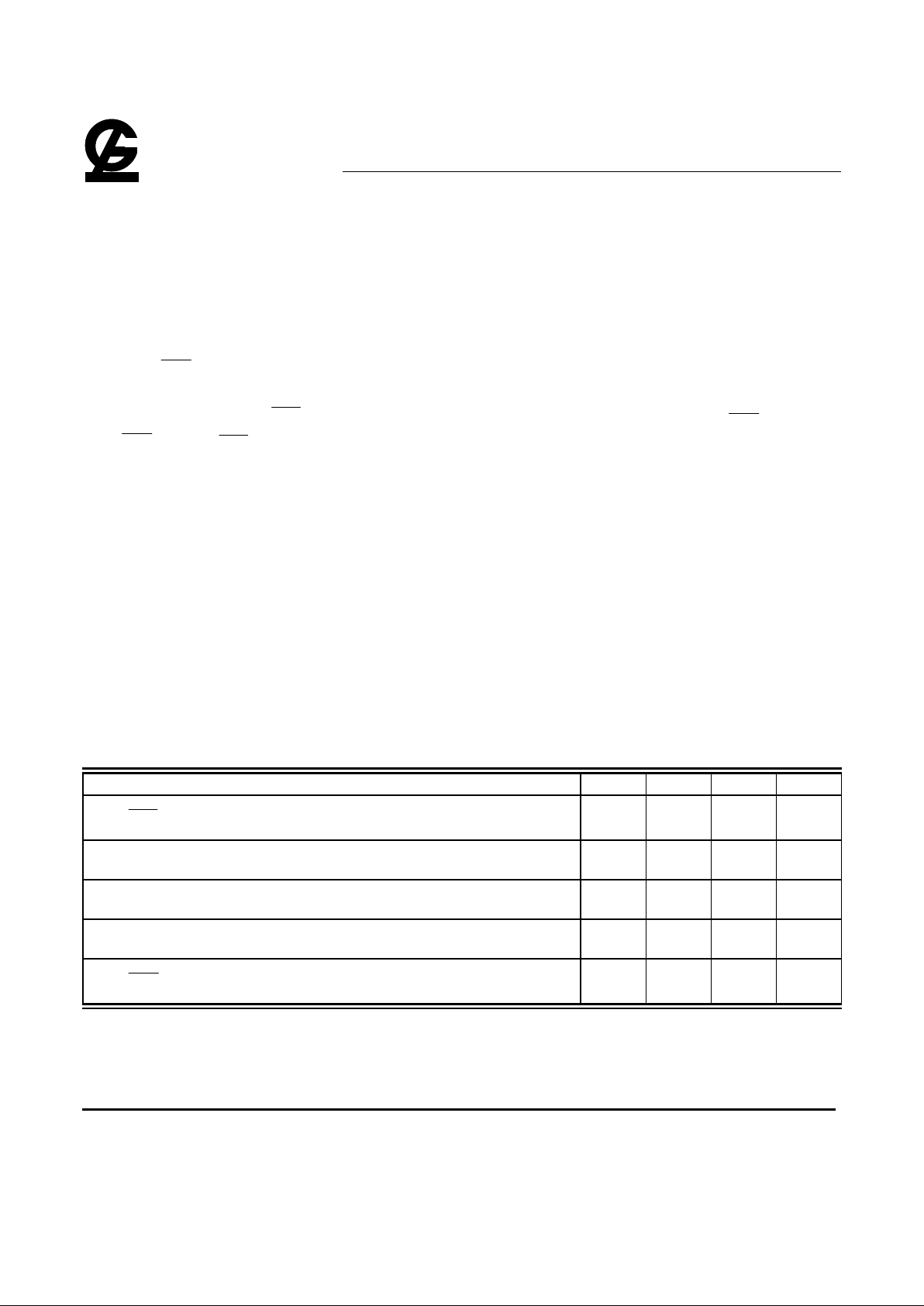
HIGH PERFORMANCE 35 40 50
60
Max.
RAS
Access Time, (t
RAC
)
35 ns 40 ns 50 ns
60 ns
Max. Column Address Access Time, (t
CAA
) 18 ns 20 ns 25 ns
30 ns
Min. Extended Data Out Page Mode Cycle Time, (tPC) 13 ns 15 ns 20 ns
25 ns
Min. Read/Write Cycle Time, (tRC) 65 ns 70 ns 85 ns
104 ns
Max.
CAS
Access Time (t
CAC
)
11 ns 12 ns 14 ns
15 ns
Page 2
G-LINK
GLT4160L16
1M X 16 CMOS DYNAMIC RAM WITH EXTENDED DATA OUTPUT
Mar 2000 (Rev.2.0)
G-Link Technology Corporation
2701Northwestern Parkway
Santa Clara, CA 95051, U.S.A.
G-Link Technology Corporation,Taiwan
6F, No. 24-2, Industry E. RD. IV, Science Based
Industrial Park, Hsin Chu, Taiwan.
- 2 -
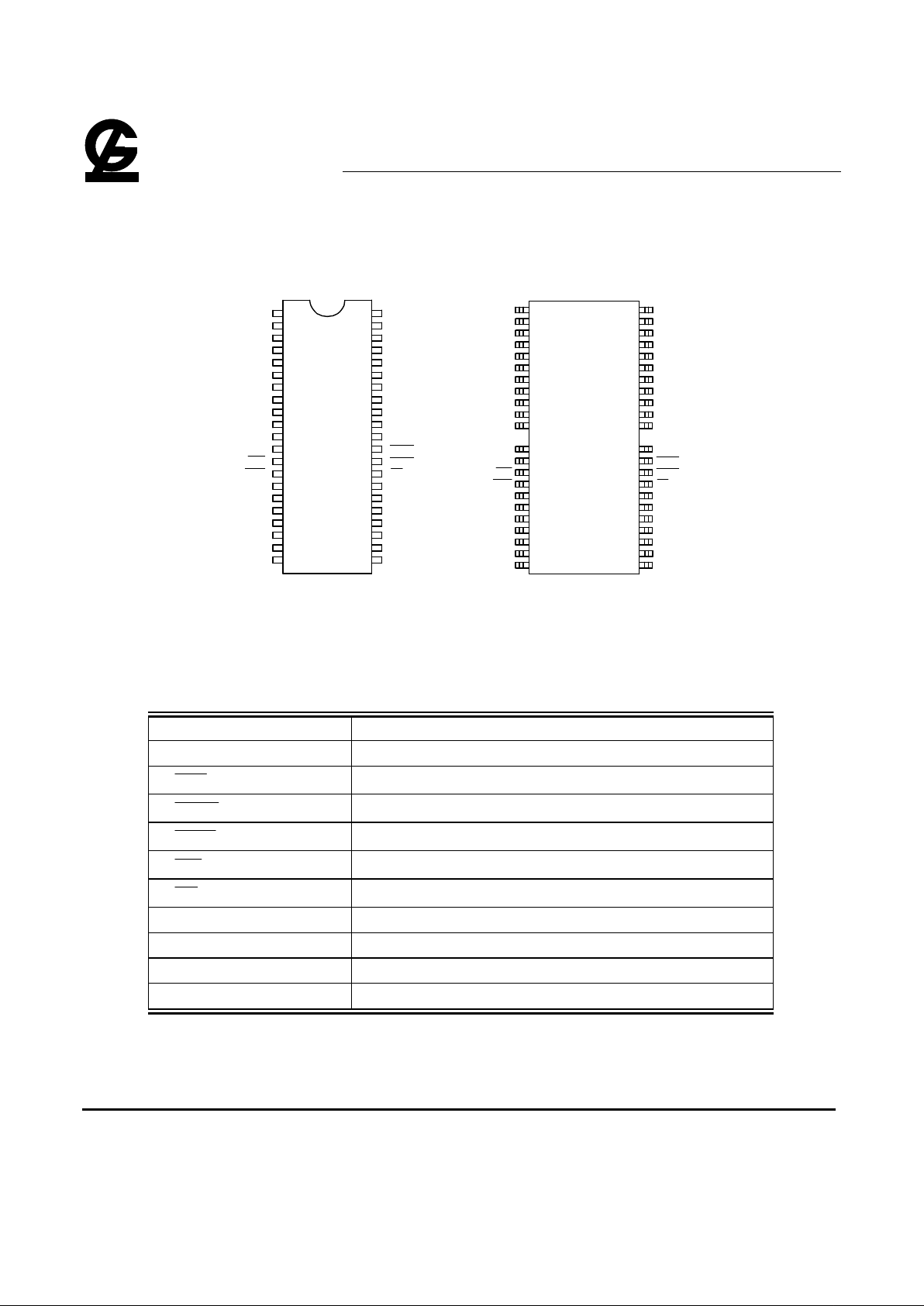
Pin Configuration :
Vcc
DQ0
A0
A1
1
2
3
4
5
6
7
9
10
11
12
13
NC
OE
LCAS
VSS
DQ15
DQ1
WE
RAS
NC
A9
A8
8
14
15
16
17
18
19
20 23
24
25
26
27
28
29
30
31
32
33
34
35
36
37
38
39
40
41
42
DQ2
DQ
3
Vcc
DQ4
DQ5
DQ6
DQ7
NC
A2
DQ14
DQ13
DQ
12
VSS
DQ11
DQ10
DQ9
DQ8
UCAS
A7
A6
A
5
GLT416016
SOJ Top View
VCC 21 VSS22
NC
NC
A3 A
4
Vcc
DQ0
A0
A1
1
2
3
4
5
6
7
9
10
12
13
14
NC
OE
LCAS
VSS
DQ15
DQ1
WE
RAS
NC
A9
A8
8
15
16
17
18
19
20
21 24
25
26
27
28
29
30
31
32
33
35
36
37
38
39
40
41
42
43
44
DQ2
DQ3
Vcc
DQ4
DQ5
DQ6
DQ7
NC
A2
DQ14
DQ13
DQ12
VSS
DQ11
DQ10
DQ9
DQ8
UCAS
A7
A6
A5
TSOP(Type II)
Top View
VCC 22 23 VSS
3411NC
NC
NC
A3
NC
A4
Pin Descriptions:
Name Function
A0 - A
9
Address Inputs
RAS
Row Address Strobe
UCAS
Column Address Strobe/Upper Byte Control
LCAS
Column Address Strobe/Lower Byte Control
WE
Write Enable
OE
Output Enable
DQ0 - DQ
15
Data Inputs / Outputs
V
CC
+3.3V Power Supply
V
SS
Ground
NC No Connection
Page 3
G-LINK
GLT4160L16
1M X 16 CMOS DYNAMIC RAM WITH EXTENDED DATA OUTPUT
Mar 2000 (Rev.2.0)
G-Link Technology Corporation
2701Northwestern Parkway
Santa Clara, CA 95051, U.S.A.
G-Link Technology Corporation,Taiwan
6F, No. 24-2, Industry E. RD. IV, Science Based
Industrial Park, Hsin Chu, Taiwan.
- 3 -
Absolute Maximum Ratings* Capacitance*
TA=25°C, VCC=3.3V±0.3V, VSS=0V
Operating Temperature, TA (ambient)
.....................................…0°C to +70°C
Storage Temperature(plastic)....-55°C to +150°C
Voltage Relative to VSS...............-1.0V to + 4.6V
Short Circuit Output Current......................50mA
Power Dissipation......................................1.0W
Symbol
C
IN1
C
IN2
C
OUT
Parameter
Address Input
RAS,LCAS
,
UCAS
,WE,
OE
Data Input/Output
Max.
5
7
7
Unit
pF
pF
pF
*Note:Operation above Absolute Maximum Ratings can
abversely affect device reliability.
*Note: Capacitance is sampled and not 100% tested
Electrical Specifications
l
CAS
means
UCAS
and
LCAS
.
l All voltages are referenced to GND.
l After power up, wait more than 100µs and then, execute eight
CAS
-before-
RAS
or
RAS
-only
refresh cycles as dummy cycles to initialize internal circuit.
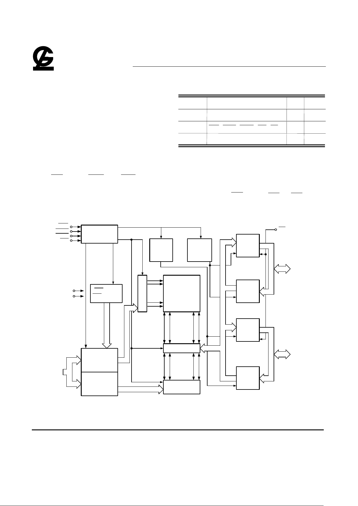
Block Diagram :
Memory
Array
1024X1024X16
Upper
Byte
Control
Sense Amplifier
Column Decoder
Row
Address
Buffer
Column
Address
Buffer
...1024X16...
...1024...
....1024....
Lower
Byte
Control
Row Decoder
Data
Output
Buffer
Data
Input
Buffer
Data
Output
Buffer
Data
Input
Buffer
CAS before
RAS Counter
Clock
Generator
A0
|
A9
X0..X9
Y0..Y9
DQ8
|
DQ15
DQ0
|
DQ7
RAS
LCAS
UCAS
WE
Vcc
GND
OE
X8
X8
X8
X8
X8
X1
6
X8
X8
X8
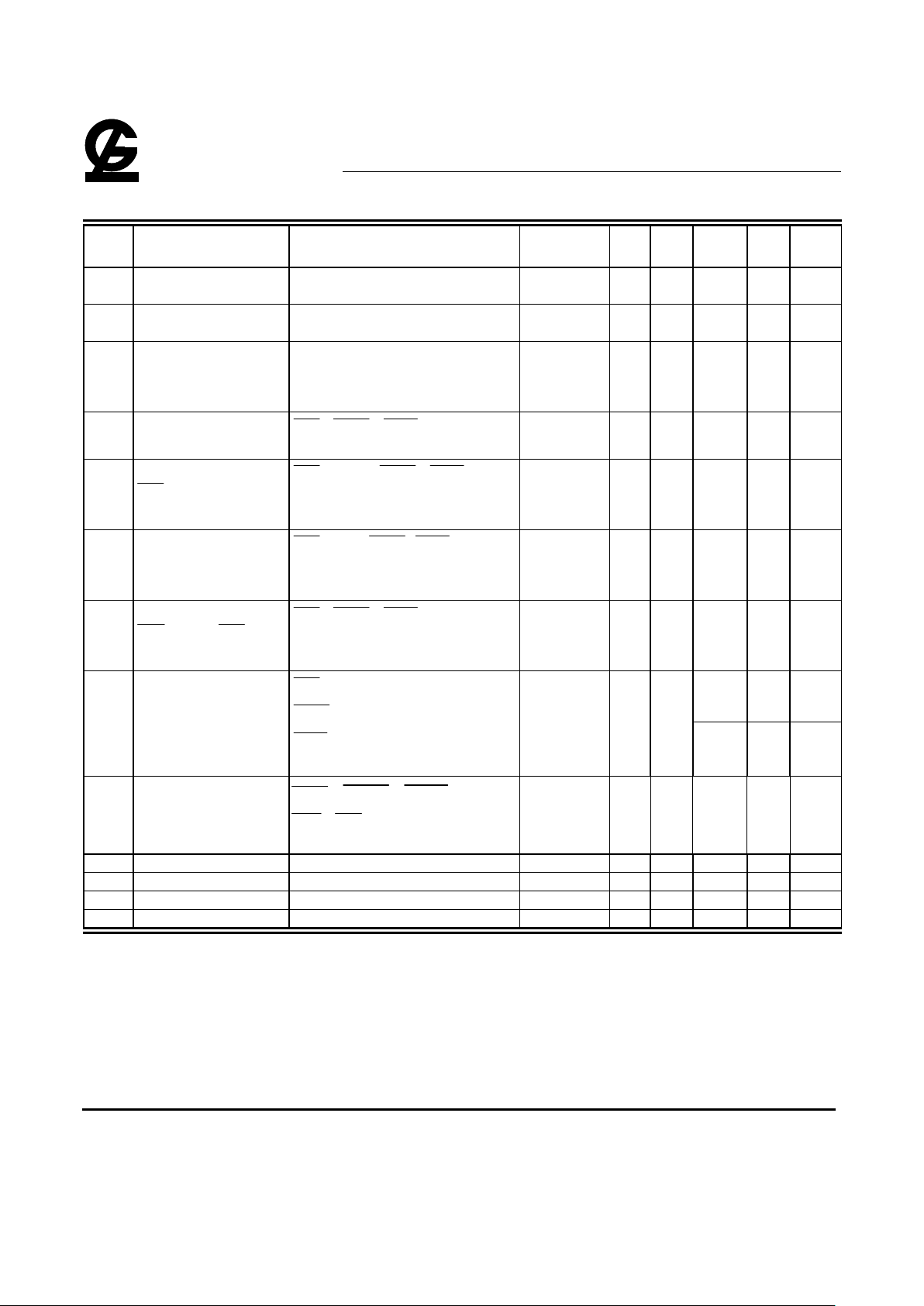
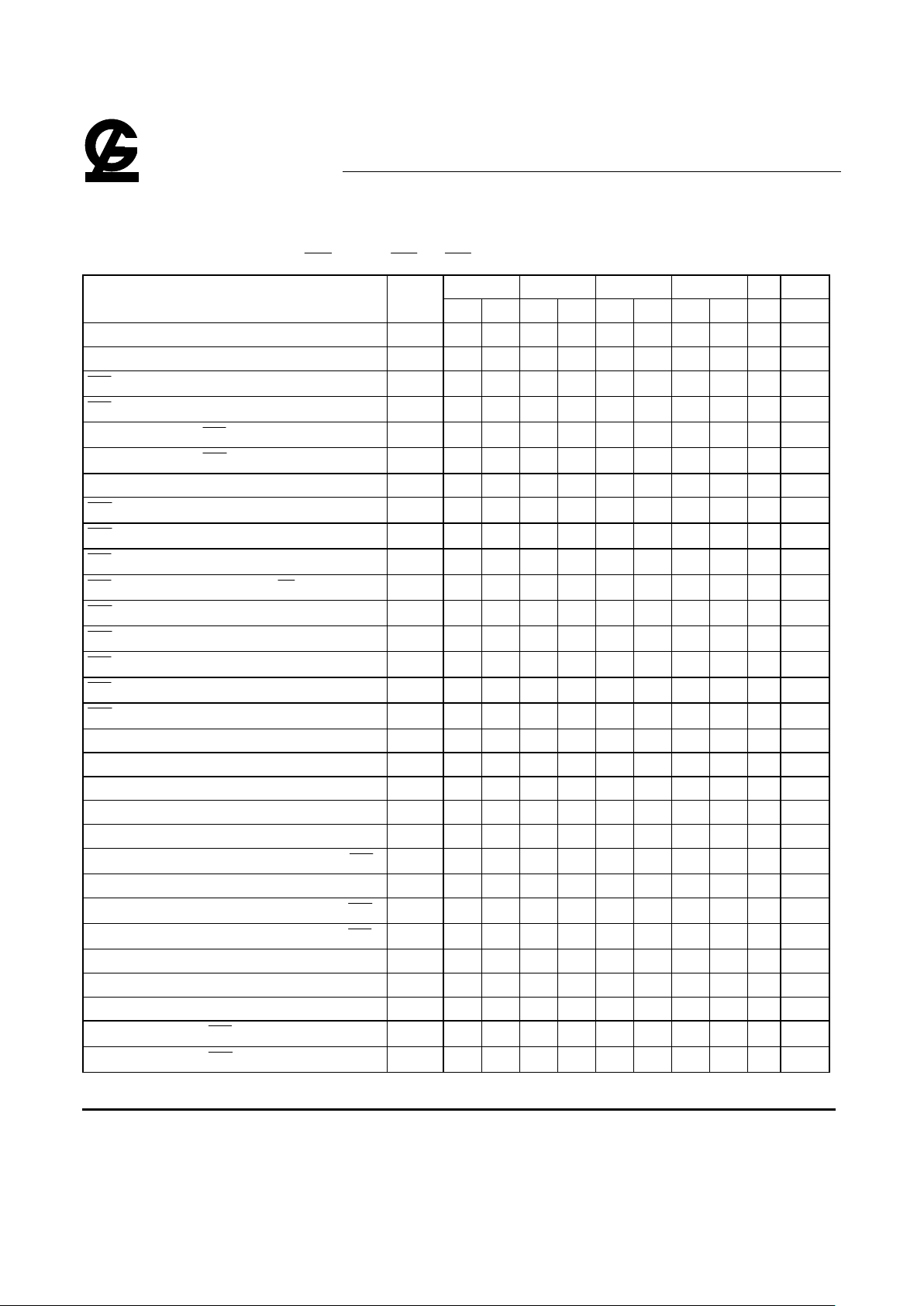
DC and Operating Characteristics (1-2)
Page 4
G-LINK
GLT4160L16
1M X 16 CMOS DYNAMIC RAM WITH EXTENDED DATA OUTPUT
Mar 2000 (Rev.2.0)
G-Link Technology Corporation
2701Northwestern Parkway
Santa Clara, CA 95051, U.S.A.
G-Link Technology Corporation,Taiwan
6F, No. 24-2, Industry E. RD. IV, Science Based
Industrial Park, Hsin Chu, Taiwan.
- 4 -
TA = 0°C to 70°C, VCC=3.3V±0.3V, VSS=0V, unless otherwise specified.
Sym. Parameter Test Conditions Access
Time
Min. Typ Max. Unit Notes
I
LI
Input Leakage Current
(any input pin)
0V ≤ V
IN
≤ Vcc+0.3V
(All other pins not under test=0V)
-5 +5
µA
I
LO
Output Leakage Current
(for High-Z State)
0V ≤ V
out
≤ Vcc
Output is disabled (Hiz)
-5 +5
µA
I
CC1
Operating Current,
Random READ/WRITE tRC = tRC (min.)
t
RAC
= 35ns
t
RAC
= 40ns
t
RAC
= 50ns
t
RAC
= 60ns
170
160
150
140
mA 1,2
I
CC2
Standby Current,(TTL)
RAS, UCAS
,
LCAS
at V
IH
other inputs ≥V
SS
1 mA
I
CC3
Refresh Current,
RAS
-Only
RAS
cycling,
UCAS
,
LCAS
at V
IH
tRC = tRC (min.)
t
RAC
= 35ns
t
RAC
= 40ns
t
RAC
= 50ns
t
RAC
= 60ns
170
160
150
140
mA 2
I
CC4
Operating Current,
EDO Page Mode
RAS
at VIL,
UCAS
,
LCAS
address
cycling:tPC=tPC(min.)
t
RAC
= 35ns
t
RAC
= 40ns
t
RAC
= 50ns
t
RAC
= 60ns
170
160
150
140
mA 1,2
I
CC5
Refresh Current,
CAS
Before
RAS
RAS, UCAS
,
LCAS
address cycling:
tRC=tRC (min.)
t
RAC
= 35ns
t
RAC
= 40ns
t
RAC
= 50ns
t
RAC
= 60ns
170
160
150
140
mA 1
0.5 mA 1I
CC6
Standby Current,
(CMOS)
RAS
≥VCC-0.2V,
UCAS
≥VCC-0.2V,
LCAS
≥VCC-0.2V,
All other inputs V
SS
200
µA
1,5
I
CC7
Self Refresh Current
RAS =
UCAS = LCAS =V
IL
WE = OE =A0~A9=VCC-0.2V or 0.2V
DQ0~DQ15=VCC-0.2V,0.2V or Open
200
µA
V
IL
Input Low Voltage -0.3 +0.8 V 3
V
IH
Input High Voltage 2.0 VCC+0.3 V 3
V
OL
Output Low Voltage IOL = 2mA 0.4 V
V
OH
Output High Voltage IOH = -2mA 2.4 V
Notes:
1.ICC is dependent on output loading when the device output is selected. Specified ICC(max.) is measured with the output open.
2.ICC is dependent upon the number of address transitions specified ICC(max.) is measured with a maximum of one transition per address cycle in
random Read/Write and EDO Fast Page Mode.
3.Specified VIL(min.) is steady state operation. During transitions VIL(min.) may undershoot to -1.0V for a period not to exceed 15ns. All AC
parameters are measured with VIL(min.)≥VSS and VIH(max.)≤VCC.
4.Specified VIH(max.) is steady state operation. During transitions VIH(max.) may undershoot to +1.0V for a period not to exceed 15ns. All AC
parameters are measured with VIL(min.)≥VSS and VIH(max.)≤VCC.
5.S-Version.
Page 5
G-LINK
GLT4160L16
1M X 16 CMOS DYNAMIC RAM WITH EXTENDED DATA OUTPUT
Mar 2000 (Rev.2.0)
G-Link Technology Corporation
2701Northwestern Parkway
Santa Clara, CA 95051, U.S.A.
G-Link Technology Corporation,Taiwan
6F, No. 24-2, Industry E. RD. IV, Science Based
Industrial Park, Hsin Chu, Taiwan.
- 5 -
AC Characteristics
TA = 0°C to 70°C , VCC = 3V ±0.3V, VIH / VIL = 3.0/0 V, VOH/VOL = 2.0/0.8V
An initial pause of 100 µs and 8
CAS
-before-
RAS
or
RAS
-only refresh cycles are required after power-up.
35 40 50 60
Parameter Symbol Min. Max. Min. Max. Min. Max. Min. Max. Unit Notes
Read or Write Cycle Time
t
RC
65 70 85 104 ns
Read Modify Write Cycle Time
t
RWC
86 91 106 133 ns
RAS Precharge Time
t
RP
25 25 30 40 ns
RAS Pulse Width
t
RAS
35 100K 40 100K 50 100K 60 100k ns
Access Time from RAS
t
RAC
35 40 50 60 ns 1,2,3
Access Time from CAS
t
CAC
11 12 14 15 ns 1,5,10
Access Time from Column Address
t
AA
18 20 25 30 ns 1,5,6
CAS to Output Low-Z
t
CLZ
0 0 0 0 ns
CAS to Output High-Z
t
CEZ
3 8 3 8 3 8 3 10 ns
RAS Hold Time
t
RSH
12 12 14 13 ns
RAS Hold Time Referenced to OE
t
ROH
8 8 9 10 ns
CAS Hold Time
t
CSH
30 34 45 40 ns
CAS Pulse Width
t
CAS
6 10k 6 10k 8 10k 12 10k ns
RAS to CAS Delay Time
t
RCD
17 24 18 28 19 37 18 45 ns
RAS to Column Address Delay Time
t
RAD
12 17 13 20 14 25 13 30 ns 7
CAS to RAS Precharge Time
t
CRP
5 5 5 5 ns
Row Address Set-Up Time
t
ASR
0 0 0 0 ns
Row Address Hold Time
t
RAH
7 8 9 10 ns
Column Address Set-Up Time
t
ASC
0 0 0 0 ns
Column Address Hold Time
t
CAH
6 6 7 10 ns
Column Address to RAS Lead Time
t
RAL
18 20 25 30 ns
Column Address Hold Time Referenced to RAS
t
AR
30 34 44 55 ns
Read Command Set-Up Time
t
RCS
0 0 0 0 ns
Read Command Hold Time Referenced to CAS
t
RCH
0 0 0 0 ns 4
Read Command Hold Time Referenced to RAS
t
RRH
0 0 0 0 ns 4
Write Command Set-Up Time
t
WCS
0 0 0 0 ns 8,9
Write Command Hold Time
t
WCH
6 6 6 10 ns
Write Command Pulse Width
t
WP
6 6 6 10 ns
Write Command to RAS Lead Time
t
RWL
11 12 13 13 ns
Write Command to CAS Lead Time
t
CWL
11 12 13 13 ns
Page 6

G-LINK
GLT4160L16
1M X 16 CMOS DYNAMIC RAM WITH EXTENDED DATA OUTPUT
Mar 2000 (Rev.2.0)
G-Link Technology Corporation
2701Northwestern Parkway
Santa Clara, CA 95051, U.S.A.
G-Link Technology Corporation,Taiwan
6F, No. 24-2, Industry E. RD. IV, Science Based
Industrial Park, Hsin Chu, Taiwan.
- 6 -
AC Characteristics
35 40 50 60
Parameter Symbol Min. Max. Min. Max. Min. Max. Min. Max. Unit Notes
Data Set-Up Time
t
DS
0 0 0 0 ns
Data Hold Time
t
DH
7 7 8 10 ns
Data Hold Time Referenced to RAS
t
DHR
31 36 46 55 ns
RAS to WEE Delay Time
t
RWD
49 54 64 79 ns
CAS to WE Delay Time
t
CWD
23 24 25 32 ns
Column Address to WE Delay Time
t
AWD
30 32 37 47 ns
RAS to CAS Precharge Time
t
RPC
0 0 0 0 ns
Access Time from CAS Precharge
t
CPA
20 22 30 32 ns
EDO Page Mode Cycle Time
t
PC
13 15 20 25 ns
EDO Page Mode Read-Modify-Write Cycle Time
t
PRWC
47 50 59 63 ns
CAS Precharge Time (EDO Page Mode)
t
CP
5 5 8 15 ns
RAS Pulse Width (EDO Page Mode Only)
t
RASP
35 100K 40 100K 50 100K 60 100k ns
Access Time from OE
t
OEA
11 12 14 15 ns
OE to Data Delay Time
t
OED
8 8 8 13 ns
OE to Output High-Z
t
OEZ
3 8 3 8 3 8 3 8 ns
OE Command Hold Time
t
OEH
6 7 7 0 ns
Data Output Hold after CAS low
t
DOH
3 3 5 5 ns
RAS to Output High-Z
t
REZ
3 8 3 8 3 8 3 8 ns
WE to Output High-Z
t
WEZ
3 10 3 10 3 12 3 12 ns
OE to CAS Hold Time
t
OCH
8 8 8 5 ns
CAS Hold Time to OE
t
CHO
8 8 8 5 ns
OE Precharge Time
t
OEP
8 8 8 5 ns
CAS Set-Up Time for CAS -before-RAS Cycle
t
CSR
10 10 10 10 ns
CAS Hold Time for CAS -before-RAS Cycle
t
CHR
8 8 10 10 ns
Transition Time
t
T
1.5 50 1.5 50 2 50 2 50 ns
Refresh Period
t
REF
16 16 16 16 ms
RAS pulse width
(
CAS
-before-RAS
Self
refresh)
t
RASS
100 100 100 100
µs
RAS precharge time
(
CAS
-before-RAS
Self refresh)
t
RPS
60 70 90 110 ns
CAS
precharge time
(
CAS
-before-RAS
Self refresh)
t
CHS
-50 -50 -50 -50 ns
Page 7

G-LINK
GLT4160L16
1M X 16 CMOS DYNAMIC RAM WITH EXTENDED DATA OUTPUT
Mar 2000 (Rev.2.0)
G-Link Technology Corporation
2701Northwestern Parkway
Santa Clara, CA 95051, U.S.A.
G-Link Technology Corporation,Taiwan
6F, No. 24-2, Industry E. RD. IV, Science Based
Industrial Park, Hsin Chu, Taiwan.
- 7 -
Notes:
1. Measure with a load equivalent to one TTL inputs and 50 pF.
2. Assumes that t
RCD
≤ t
RCD
(max.). If t
RCD
is greater than t
RCD
(max.), access time will be t
AA
dominant.
3. Assumes that t
RAD
≤ t
RAD
(max.). If t
RAD
is greater than t
RCD
(max.), access time will be
controlled by t
CAC
.
4. Either t
RRH
or t
RCH
must be satisfied for a Read Cycle.
5. Access time is determined by the longest of t
CAA
, t
CAC
and t
CPA
.
6. Assumes that t
RAD
≥ t
RAD
(max.).
7. Operation within the t
RAD
(max.) limit ensures that t
RAC
(max.) can be met. t
RAD
(max.)
is specified as a reference point only. If t
RAD
is greater than the specified t
RAD
(max.)
limit, the access time is controlled by t
CAA
and t
CAC
.
8. t
WCS
, t
RWD
, t
AWD
and t
CWD
are not restrictive operating parameters.
9. t
WCS
(min.) must be satisfied in an Early Write Cycle.
10. tDS and tDH are referenced to the latter occurrence of
CAS
of
WE
.
11. tT is measured between VIH (min.) and VIL (max.). AC-measurements assume tT = 1.5 ns.
Page 8

G-LINK
GLT4160L16
1M X 16 CMOS DYNAMIC RAM WITH EXTENDED DATA OUTPUT
Mar 2000 (Rev.2.0)
G-Link Technology Corporation
2701Northwestern Parkway
Santa Clara, CA 95051, U.S.A.
G-Link Technology Corporation,Taiwan
6F, No. 24-2, Industry E. RD. IV, Science Based
Industrial Park, Hsin Chu, Taiwan.
- 8 -
Read CYCLE Note : D
IN
= OPEN
ROW
ADDRESS
COLUMN
ADDRESS
DATA-OUT
t
RC
tRAS
tRP
tCRP
tCSH
tRCD tRSH
tCAS
tCRP
tASR tRAH
tRAD
tASC
tCAH
tRAL
t
RCH
t
RRH
t
AR
t
RCS
tAA
t
OEA
t
CEZ
tOEZ
t
CAC
tCLZ
tRAC
Don't Care
V
IH-
V
IL-
RAS
V
IH-
V
IL-
UCAS,LCAS
V
IH-
V
IL-
Address
V
IH-
V
IL-
WE
V
IH-
V
IL-
OE
V
OH-
V
OL-
DQ
Early Write Cycle NOTE : D
OUT
= OPEN
t
RP
t
RC
tCRP
tCSH
t
CRP
tRCD t
RSH
tCAS
tASR
t
RAH
t
RAD
t
ASC
tCAH
t
RAL
tCWL
tRWL
tWCR
tWCH
t
WP
tWCS
t
AR
tDS t
DH
tDHR
DATA - IN
COLUMN
ADDRESS
ROW
ADDRESS
VIH-
VIL-
RAS
VIH-
VIL-
UCAS,LCAS
VIH-
VIL-
Address
VIH-
VIL-
WE
VIH-
VIL-
OE
VIH-
VIL-
DQ
Don't Care
tRAS
Page 9

G-LINK
GLT4160L16
1M X 16 CMOS DYNAMIC RAM WITH EXTENDED DATA OUTPUT
Mar 2000 (Rev.2.0)
G-Link Technology Corporation
2701Northwestern Parkway
Santa Clara, CA 95051, U.S.A.
G-Link Technology Corporation,Taiwan
6F, No. 24-2, Industry E. RD. IV, Science Based
Industrial Park, Hsin Chu, Taiwan.
- 9 -
OE Controlled Write Cycle NOTE : D
OUT
= OPEN
tRP
t
RC
tCRP
t
CSH
tCRP
tRCD tRSH
t
CAS
tASR
t
RAH
tRAD
tASC
tCAH
tRAL
DATA - IN
COLUMN
ADDRESS
ROW
ADDRESS
VIH-
VIL-
RAS
VIH-
VIL-
UCAS,LCAS
VIH-
VIL-
Address
VIH-
VIL-
WE
VIH-
VIL-
OE
V
IH-
V
IL-
DQ
Don't Care
tRAS
tRCS
tCWL
tRWL
tWP
tDS
t
OED
tOEH
t
DH
Read - Modify - Write Cycle
tRP
t
RC
tCRP
tCRP tRCD
tRSH
VALID
DATA-OUT
COLUMN
ADDRESS
ROW
ADDR.
V
IH-
V
IL-
RAS
V
IH-
V
IL-
UCAS,LCAS
V
IH-
V
IL-
Address
V
IH-
V
IL-
WE
V
IH-
V
IL-
OE
V
I/OH-
V
I/OL-
DQ
Don't Care
tRAS
VALID
DATA-IN
tCAS
t
ASR
tRAH
tRAD
tASC
tCAH
t
CSH
tAWD
tCWD
tRWL
tCWL
tWP
tOEA
t
CLZ
tCAC
tAA
tRAC
tDH
tDS
tOED
tOEZ
Page 10

G-LINK
GLT4160L16
1M X 16 CMOS DYNAMIC RAM WITH EXTENDED DATA OUTPUT
Mar 2000 (Rev.2.0)
G-Link Technology Corporation
2701Northwestern Parkway
Santa Clara, CA 95051, U.S.A.
G-Link Technology Corporation,Taiwan
6F, No. 24-2, Industry E. RD. IV, Science Based
Industrial Park, Hsin Chu, Taiwan.
- 10 -
EDO Page Mode Read Cycle
t
RASP
t
RP
t
CRP
t
RCDtCAS
t
CSH
t
CP
t
CAS
t
CAS
t
CAS
t
CP
t
CP
t
PC
t
PC
t
PC
t
CSR
t
RAH
t
RAD
t
ASC
t
ASC
t
ASC
t
ASC
t
CAH
t
CAH
t
CAH
t
CAH
t
RCS
t
RCH
t
RRH
t
OEA
t
OEA
t
CAC
t
CPA
t
AA
t
OCH
t
CPA
t
AA
t
CAC
t
OEP
t
CHO
t
AA
t
CAC
t
CPA
t
CLZ
t
OLZ
t
RAC
t
CAC
t
DOH
t
OEZ
t
OEP
t
OEZ
t
OEZ
VALID
DATA-OUT
VALID
DATA-OUT
VALID
DATA-OUT
VALID
DATA-OUT
VALID
DATA-OUT
V
IH-
V
IL-
RAS
V
IH-
V
IL-
UCAS,LCAS
V
IH-
V
IL-
Address
V
IH-
V
IL-
WE
V
IH-
V
IL-
OE
DQ
V
OH-
V
OL-
ROW
ADDR.
COLUMN
ADDRESS
COLUMN
ADDRESS
COL.
ADDR.
COL.
ADDR.
Don't Care
EDO Page Mode Early Write Cycle NOTE : D
OUT
= OPEN
t
RASP
t
RP
t
CRP
t
RCDtCAS
V
IH-
V
IL-
RAS
V
IH-
V
IL-
UCAS,LCAS
t
CAS
t
CAS
t
CP
t
CP
t
PC
t
PC
t
RSH
t
ASR
t
RAD
t
RAH
t
ASC
t
CAH
t
CSH
t
ASC
t
ASC
t
CAH
t
CAH
t
WCS
t
WP
t
WCH
t
WCS
t
WCS
t
WCH
t
WCH
t
WP
t
WP
t
DS
t
DS
t
DS
t
DH
t
DS
t
DS
V
IH-
V
IL-
Address
V
IH-
V
IL-
WE
V
IH-
V
IL-
OE
DQ
V
IH-
V
IL-
ROW
ADDR.
COLUMN
ADDRESS
COLUMN
ADDRESS
COLUMN
ADDRESS
VALID
DATA-IN
VALID
DATA-IN
VALID
DATA-IN
Don't Care
Page 11

G-LINK
GLT4160L16
1M X 16 CMOS DYNAMIC RAM WITH EXTENDED DATA OUTPUT
Mar 2000 (Rev.2.0)
G-Link Technology Corporation
2701Northwestern Parkway
Santa Clara, CA 95051, U.S.A.
G-Link Technology Corporation,Taiwan
6F, No. 24-2, Industry E. RD. IV, Science Based
Industrial Park, Hsin Chu, Taiwan.
- 11 -
EDO Page Mode Read - Modify - Write Cycle
t
RASP
t
RP
V
IH-
V
IL-
RAS
V
IH-
V
IL-
UCAS,LCAS
Don't Care
t
CSH
t
RCD
t
CAS
t
CP
t
CAS
t
RSH
t
CRP
t
RAD
t
RAH
t
ASR
t
ASC
t
CAH
t
ASC
t
CAH
t
RAL
t
PRWC
t
RCS
t
WP
t
CWL
t
WP
t
CWL
t
RWL
t
CWD
t
AWD
t
RWD
t
OEA
t
CWD
t
AWD
t
CPWD
t
OEA
t
OEH
t
RAC
t
AA
t
CAC
t
OEZ
t
OED
t
DS
t
DH
t
AA
t
CAC
t
OEZ
t
OED
t
DS
t
DH
t
CLZ
t
CLZ
VALID
DATA-OUT
VALID
DATA-IN
VALID
DATA-OUT
VALID
DATA-IN
ROW
ADDR.
COL.
ADDR.
COL.
ADDR.
V
IH-
V
IL-
Address
V
IH-
V
IL-
WE
V
IH-
V
IL-
OE
V
I/OH-
V
I/OL-
DQ
CAS - Before - RAS Refresh Cycle
V
IH-
V
IL-
RAS
t
RAS
t
RAS
t
RP
t
RP
t
RC
t
RC
t
CSR
t
CSR
t
CHR
t
CHR
t
RPC
t
RPCtCRP
V
IH-
V
IL-
UCAS,LCAS
Remark Address, WE, OE : Don’t care DQ : Hi-Z
RAS -Only Refresh Cycle
V
IH-
V
IL-
RAS
t
RAS
t
RAS
t
RP
t
RP
t
RC
t
RC
t
RPC
t
CRP
V
IH-
V
IL-
UCAS,LCAS
t
CRP
t
ASR
t
ASR
t
RAH
t
RAH
ROW
ADDRESS
ROW
ADDRESS
Address
V
IH-
V
IL-
Remark WE, OE : Don’t care DQ : Hi-Z
Page 12

G-LINK
GLT4160L16
1M X 16 CMOS DYNAMIC RAM WITH EXTENDED DATA OUTPUT
Mar 2000 (Rev.2.0)
G-Link Technology Corporation
2701Northwestern Parkway
Santa Clara, CA 95051, U.S.A.
G-Link Technology Corporation,Taiwan
6F, No. 24-2, Industry E. RD. IV, Science Based
Industrial Park, Hsin Chu, Taiwan.
- 12 -
CAS
- Before -
RAS
Self Refresh Cycle
V
IH-
V
IL-
RAS
t
CP
tRPt
RASS
t
CP
t
CHS
V
IH-
V
IL-
UCAS
t
CSR
V
IH-
V
IL-
LCAS
t
CHS
t
RPC
t
RPC
t
CP
t
CSR
t
CEZ
OPEN
OPEN
V
IH-
V
IL-
DQ0~DQ
7
V
IH-
V
IL-
DQ8~DQ
15
Don't Care
NOTE : WE , OE ,Address = Don’t care.
Hidden Refresh Cycle ( Read )
tRP
tCRP
tRCD
VIH-
VIL-
RAS
VIH-
VIL-
UCAS,LCAS
t
RAC
V
IH-
V
IL-
Address
VIH-
VIL-
WE
VIH-
VIL-
OE
DQ
VIH-
VIL-
ROW
ADDRESS
Don't Care
tRP
t
CAC
tRCS
tASC
tCAHtASR
tCAH
tRAD
tRAL
tRSH tCHR
t
RC
tRAS tRAS
COLUMN
ADDRESS
t
RC
tWHR
tAA
tOEA
tCLZ
tREZ
tCEZ
tWEZ
t
OEZ
DATA-OUT
OPEN
Page 13

G-LINK
GLT4160L16
1M X 16 CMOS DYNAMIC RAM WITH EXTENDED DATA OUTPUT
Mar 2000 (Rev.2.0)
G-Link Technology Corporation
2701Northwestern Parkway
Santa Clara, CA 95051, U.S.A.
G-Link Technology Corporation,Taiwan
6F, No. 24-2, Industry E. RD. IV, Science Based
Industrial Park, Hsin Chu, Taiwan.
- 13 -
Hidden Refresh Cycle ( Write ) NOTE : D
OUT
= OPEN
tRP
tCRP tRCD
VIH-
VIL-
RAS
VIH-
VIL-
UCAS,LCAS
tDS
VIH-
VIL-
Address
VIH-
VIL-
WE
V
IH-
V
IL-
OE
DQ
VIH-
VIL-
ROW
ADDRESS
Don't Care
tRP
tDH
tWP
tWCH
tWCS
tASC
tCAHtASC
tCAH
tRAD t
RSH
tRSH tCHR
t
RC
tRAS tRAS
COLUMN
ADDRESS
DATA-IN
Page 14

G-LINK
GLT4160L16
1M X 16 CMOS DYNAMIC RAM WITH EXTENDED DATA OUTPUT
Mar 2000 (Rev.2.0)
G-Link Technology Corporation
2701Northwestern Parkway
Santa Clara, CA 95051, U.S.A.
G-Link Technology Corporation,Taiwan
6F, No. 24-2, Industry E. RD. IV, Science Based
Industrial Park, Hsin Chu, Taiwan.
- 14 -
CAS –Before- RAS Refresh Counter Test Cycle
t
CAS
t
CPT
VIH-
VIL-
RAS
VIH-
V
IL-
CAS
t
RP
t
RAS
t
CSR
t
CHR
t
RSH
t
RAL
t
ASC
t
AA
t
CAC
t
RCS
t
RRH
t
RCH
t
OEA
t
CEZ
t
OEZ
t
CLZ
t
RWL
t
CWL
t
WCH
t
WCS
t
WP
t
DS
t
DH
t
RCS
t
AWD
t
CWD
t
RWL
t
CWL
t
WP
t
DH
t
DS
t
OED
t
OEZ
t
CLZ
t
CAC
t
AA
t
OEA
OPEN
COLUMN
ADDRESS
VALID DATA-OUT
VALID DATA-IN
Don't Care
VALID
DATA-IN
VALID
DATA-OUT
VIH-
VIL-
Address
VIH-
VIL-
WE
VIH-
VIL-
OE
VOH-
VOL-
DQ
VIH-
VIL-
WE
VIH-
VIL-
OE
VIH-
VIL-
DQ
V
IH-
VIL-
WE
VIH-
V
IL-
OE
VI/OH-
VI/OL-
DQ
Read Cycle
Write Cycle
Read-Modify-Write
t
CAH
Page 15

G-LINK
GLT4160L16
1M X 16 CMOS DYNAMIC RAM WITH EXTENDED DATA OUTPUT
Mar 2000 (Rev.2.0)
G-Link Technology Corporation
2701Northwestern Parkway
Santa Clara, CA 95051, U.S.A.
G-Link Technology Corporation,Taiwan
6F, No. 24-2, Industry E. RD. IV, Science Based
Industrial Park, Hsin Chu, Taiwan.
- 15 -
Ordering Information
Part Number SPEED POWER FEATURE PACKAGE
GLT4160L16-35J4 35ns Normal EDO 42L 400mil SOJ
GLT4160L16-40J4 40ns Normal EDO 42L 400mil SOJ
GLT4160L16-50J4 50ns Normal EDO 42L 400mil SOJ
GLT4160L16-60J4 60ns Normal EDO 42L 400mil SOJ
GLT4160L16-35TC 35ns Normal EDO 44/50L 400mil TSOPII
GLT4160L16-40TC 40ns Normal EDO 44/50L 400mil TSOPII
GLT4160L16-50TC 50ns Normal EDO 44/50L 400mil TSOPII
GLT4160L16-60TC 60ns Normal EDO 44/50L 400mil TSOPII
Parts Numbers (Top Mark) Definition :
GLT 4 160 L 16 - 40 J4
Note : CÙCDROM , HÙHDD.
Example :
1.GLT710008-15T 1Mbit(128Kx8)15ns 5V SRAM PDIP(300mil)Package type.
2.GLT44016-40J4 4Mbit(256Kx16)40ns 5V DRAM SOJ(400mil)Package type.
4 : DRAM
6 : Standard
SRAM
7 : Cache SRAM
8 : Synchronous
Burst SRAM
-SRAM
064 : 8K
256 : 256K
512 : 512K
100 : 1M
-DRAM
10 : 1M(C/EDO)*
11 : 1M(C/FPM)*
12 : 1M(H/EDO)*
13 : 1M(H/FPM)*
20 : 2M(EDO)
21 : 2M(FPM)
40 : 4M(EDO)
41 : 4M(FPM)
80 : 8M(EDO)
81 : 8M(FPM)
160 : 16M(EDO)
161 : 16M(FPM)
*See note
VOLTAGE
Blank : 5V
L : 3.3V
M : 2.5V
N : 2.1V
CONFIG.
04 : x04
08 : x08
16 : x16
32 : x32
SPEED
-SRAM
12 : 12ns
15 : 15ns
20 : 20ns
70 : 70ns
-DRAM
30 : 30ns
35 : 35ns
40 : 40ns
45 : 45ns
50 : 50ns
60 : 60ns
PACKAGE
T : PDIP(300mil)
TS : TSOP(Type I)
TC : TSOP(Type ll)
PL : PLCC
FA : 300mil SOP
FB : 330mil SOP
FC : 445mil SOP
J3 : 300mil SOJ
J4 : 400mil SOJ
P : PDIP(600mil)
Q : PQFP
TQ : TQFP
Page 16

G-LINK
GLT4160L16
1M X 16 CMOS DYNAMIC RAM WITH EXTENDED DATA OUTPUT
Mar 2000 (Rev.2.0)
G-Link Technology Corporation
2701Northwestern Parkway
Santa Clara, CA 95051, U.S.A.
G-Link Technology Corporation,Taiwan
6F, No. 24-2, Industry E. RD. IV, Science Based
Industrial Park, Hsin Chu, Taiwan.
- 16 -
Package Information
40/42L 400MIL SOJ
44/50L TSOPII 400MIL
 Loading...