

Page 1
Super-luminosity/High-luminosity Numeric LED
→
→
→
→
Digit
1-digit
Mold Type
Substrate
Type
Multi-digits
Mold Type
Type Type of display
Outline dimensions
Model No.
Luminous intensity
(mcd)
TYP.
Model No.
Luminous intensity
(mcd)
TYP. Page Figure
*1
Common pins
Character
height
(mm)
U (Red) T (Red)
8.0
10.16
14.12
20.32
25.4
38.1
76.0
10.16
8.0
7.6
10
9
8
6
4
3
1
12
19
21
A
K
A
K
A
K
A
K
A
K
A
K
A
K
A
K
A
K
A
K
GL9U100
GL8U100
GL9U15
GL8U15
GL9U30
GL8U30
35.0
35.0
27.0
27.0
(120)
*
(120)
*
GL9T030
GL8T030
GL9T040
GL8T040
GL9T156
GL8T156
GL9T08
GL8T08
GL9T100
GL8T100
GL7T201
GL6T201
GL3T422
GL3T421
GL3T508D
GL3T507D
4.0
4.0
4.25
4.25
5.25
5.25
2.2
2.2
9.5
9.5
4.25
4.25
1.5
1.5
1.5
1.5
*1 A: Anode common K: Cathode common * Production after order confirmation
* As for current conditions, refer to I
F in electro-optical characteristics
(Ta=25˚C)
Character height
(mm)
Forward current
IF
(mA)
Peak forward current
IFM
*1
(mA)
Derating factor
(mA/ ˚C)
Reverse voltage
VR
(V)
Operating temperature
Topr.
(˚C)
Storage temperature
Tstg.
(˚C)
Radiation
color
*1 Duty ratio=1/10, Pulse width=0.1ms
*2 U type duty ratio=1/16, pulse width=0.1ms
8.0/10.16/14.12/20.32
25.4, 38.1, 76.0
25.4, 38.1
T
U
T
20
20
20
100
150
*2
100
0.36
0.36
0.36
5
6
5
-30 to +70
-30 to +70
-30 to +70
-40 to +80
-40 to +80
-40 to +80
1.82
2.73
1.82
DC Pulse
(Ta=25˚C)
Character height
(mm)
Forward current
VF
Peak emission wavelength
λp(nm)
TYP.
Radiation
color
8.0/10.16/14.12/20.32
25.4, 38.1, 76.0
25.4, 38.1
T
U
T
1.7
3.5
3.4
2.2
4.8
4.4
660
660
660
Spectrum radiation bandwidth
∆λ(nm)
TYP.
I
F
(mA)
20
20
20
10
10
10
Reverse current
IR(µA)
MAX.
V
R
(V)
10
100
10
4
5
4
TYP. MAX
(Ta=25˚C)
■ Super-luminosity/High-luminosity Numeric LED Figures shown below are values per segment.
■ Absolute Maximum Ratings Figures shown below are values per segment.
■ Electro-optical Characteristics Figures shown below are values per segment.
(Notice) ¡
(Internet) ¡Data for sharp's optoelectronic/power device is provided for internet.(Address http://www.sharp.co.jp/ecg/)
In the absence of confirmation by device specification sheets, SHARP takes no responsibility for any defects that may occur in equipment using any SHARP
devices shown in catalogs, data books, etc. Contact SHARP in order to obtain the latest device specification sheets before using any SHARP device.
Page 2
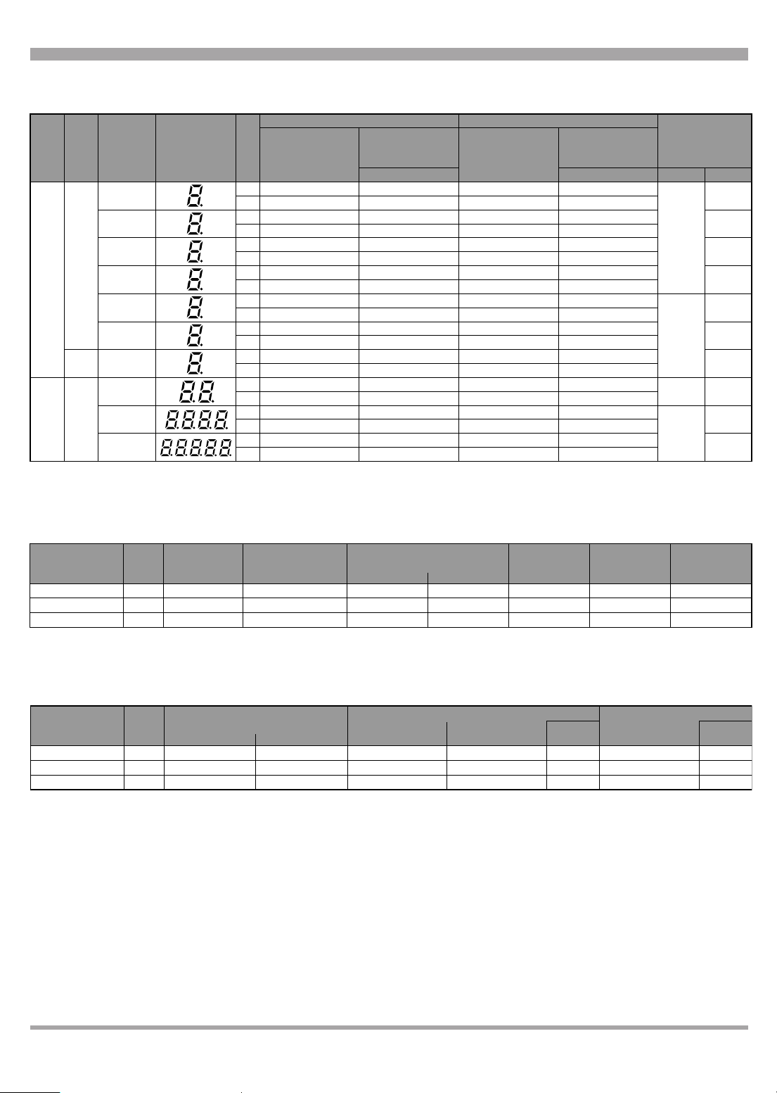
Numeric LED Characteristics Diagrams
T series
* In case of 25.4mm: value per 1segment 1chip
0
10
20
30
40
50
60
70
-20 0 20 40 60 10080
0
50
100
150
200
250
300
350
-20 0 20 40 60 10080
(Duty ratio1/10)
0.5
2
1
3
5
10
20
50
100
1.0 1.2 1.4 1.6 1.8 2.0 2.2 2.4
(T
a=25˚C)
1.1
1.3 1.5 1.7
1.9
2.1 2.3 2.5
1
2
5
200
100
20
50
10
500
0.1 0.2 0.5 1 2 5 10 20 50
(T
a=25˚C)
(1F=20mA/seg)
10
20
50
200
100
500
1000
-20 0 20 40 60 10080
5
10
30
50
100
300
500
1/50 1/20 1/10 1/5 1/2 1
(T
a=25˚C)
Forward Current Derating Curve Forward Current vs. Forward Voltage* Luminous Intensity vs. Ambient Temperature
Ambient temperature Ta(˚C) Forward voltage VF(V/seg) Ambient temperature Ta(˚C)
Forward current IF(mA/seg)
Forward current I
F(mA/seg)
Relative luminous intensity(%)
Mold type
Peak Forward Current Derating Curve Luminous Intensity vs. Forward Current Duty Ratio vs. Peak Forward Current
Ambient temperature Ta(˚C) Forward current IF(mA/seg) Duty ratio DR
Peak forward current IFM(mA/seg)
Relative luminous intensity(%)
Peak forward current I
F(mA/seg)
Mold type
Mold type
Page 3
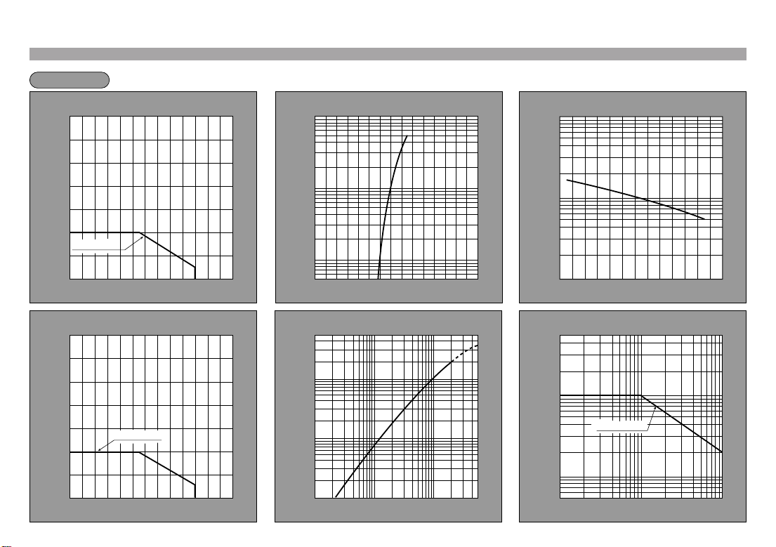
* In case of 25.4/38.1/76.0mm: value per 1segment 1chip
U series
0
10
-20 0 20 40 60 10080
1
2
0.1 0.2 0.5 1 2 5 10 20 50
5
10
1/50 1/20 1/10 1/5 1/2 1
0
5
10
15
20
25
30
35
-20 0 20 40 60 10080
0
50
100
150
-20 0 20 40 60 10080
(Duty ratio1/10)
1
2
5
200
100
20
50
10
500
0.1 0.2
0.5
12 51020 50
(T
a=25˚C)
(1F=20mA)
10
20
50
200
100
500
1000
-20 0 20 40 60 10080
150
5
10
30
50
100
300
500
1/50 1/20 1/10 1/5 1/2 1
(T
a=25˚C)
0.5
2
1
3
5
10
20
50
100
2.0 2.4 2.8 3.2 3.6 4.0 4.4 4.8
(T
a=25˚C)
2.2 2.6 3.0 3.4 3.8 4.2 4.6 5.0
Peak forward current IFM(mA/seg)
Relative luminous intensity(%)
Peak forward current I
Ambient temperature Ta(˚C) Forward current IF(mA/seg) Duty ratio DR
Mold type
Forward Current Derating Curve Forward Current vs. Forward Voltage* Luminous Intensity vs. Ambient Temperature
Ambient temperature Ta(˚C) Forward voltage VF(V/seg) Ambient temperature Ta(˚C)
Forward current IF(mA/seg)
Forward current I
F(mA/seg)
Relative luminous intensity(%)
Peak Forward Current Derating Curve Luminous Intensity vs. Forward Current Duty Ratio vs. Peak Forward Current
Ambient temperature Ta(˚C) Forward current IF(mA/seg) Duty ratio DR
Peak forward current IFM(mA/seg)
Relative luminous intensity(%)
Peak forward current I
F(mA/seg)
(Notice) ¡
(Internet) ¡Data for sharp's optoelectronic/power device is provided for internet.(Address http://www.sharp.co.jp/ecg/)
In the absence of confirmation by device specification sheets, SHARP takes no responsibility for any defects that may occur in equipment using any SHARP
devices shown in catalogs, data books, etc. Contact SHARP in order to obtain the latest device specification sheets before using any SHARP device.
Page 4

Numeric LED Outline Dimensions(Unit:mm)
D13D24E11E22F113F214G115G2
16
C2
7
D.P
.
810B29B16
C1
6-ø3.0±
0.15
Internal connection diagram
12A211
A1 D13D24E11E22F113F214G115G2
16
C2
7
D.P
.
810B29B16
C1
12A211
A1
98.0±0.5
5.08✕7mm
35.5✕
76.0±0.4
33.0±0.5 33.0±0.5
42.0±0.3
10
˚
16 9
1
55
8
8.0(Segment width)
1.3
+1.3
-0.15
0.8
76.0±0.4
45.0±0.545.0±0.5
34.0
25.0
7.5
86.0✕
7.0
7.5
D.P.
ø9.6
A
BF
EC
D
G
28.0
Segment name
(Segment width)
1
3.0
2
2-ø3.3
59.0
45.0
52.0
10.16 10.16
(2.54✕4)
Internal connection diagram
ABCD
6
24.0
1
10.16
14.5
35.0
GL9❏18
EFG
875 43210
10˚
D.P.
1.0 for all space
20.0
10
ø4.0
0.5MA✕.
BA
76
GL9❏30 Series GL8❏30 Series GL9❏18 Series GL8❏18 Series
2.54✕6=
GL9❏100
ABCD
582
9
14.7
7
˚
9.4
22.8
15.24
EFG
1412
16
D.P.
3
51.0
13.0
Internal connection diagram
4.5
38.1
21.0
7
˚
14.0
37.0
GL9❏15
ABCD
582
9
(Segment width)
3.9
17.0
ø4.8
10-ø0.55
2.54✕6=
EFG
D.P.
1412
16
15.24
Luminous intensity rank
44.0
S GL8U15
Segment name
814
A
B
F
G
E
C
D
D.P.
1
7
GL8❏15
FEG
CD
52
12114
D.P.
6
BA
89
4
33.0
MIN.
4.0 9.0
Internal connection diagram
25.4
7.5
30.5
4-ø5.5MAX.
(Calking)
(Calking)
GL8❏18
FEG
CD
D.P.
1032485
99
2.7(for all segment width)
11.2
ø3.0
ø0.55
GL8❏100
CD
BA
89
52
9.0
1.6
66.0
22.0
22.0
15.0 15.0
10.0
10.0
Segment name
F
E
D
Luminous intensity rank
27.9
S GL9E100
Segment name
814
A
B
F
G
E
C
D
71
D.P.
FEG
D.P.
12114
6
36.0
A
G
B
C
D.P.
114114
GL9❏15 Series GL8❏15 Series GL9❏100 Series GL8❏100 Series
5
25.4
33.0
7.5
Internal connection diagram
GL9❏❏100 Series GL8❏❏100 Series
(Notice) ¡
(Internet) ¡Data for sharp's optoelectronic/power device is provided for internet.(Address http://www.sharp.co.jp/ecg/)
MIN.
4.0 9.0
GL9❏❏100
(Red)
11
In the absence of confirmation by device specification sheets, SHARP takes no responsibility for any defects that may occur in equipment using any SHARP
devices shown in catalogs, data books, etc. Contact SHARP in order to obtain the latest device specification sheets before using any SHARP device.
14.7
7
˚
2.7(for all segment width)
22.8
9.4
ø0.55
2.54✕6=
15.24
BDFGC52E
A
11214
98
(Yellow-green)
4
11.2
D.P.
6
ø3.0
Luminous intensity rank
27.9
S GL9E100
Segment name
814
A
B
F
G
E
C
D
71
GL8❏❏100
A
98
(Red)
11
D.P.
BDFGC52E
11214
(Yellow-green)
4
6
27.0
20.32
11.0
7
˚
6
10
5
1
7.6
19.0
7.0
MIN.
4.0 8.0
D.P.
6
Internal connection diagram
ABCD
7
10-ø0.45
2.54✕4
=10.16
GL9❏08
EFG
46210915
GL9❏08 Series GL8❏08 Series
(Segment width)
1.8
9.26
ø2.0
BA
D.P.
67
GL8❏08
CD
42
1144 11
Luminous intensity rank
08
❏
22.86
S GL8
Segment name
A
F
B
G
C
E
D
D.P.
FEG
D.P.
9110
5
833 8
Page 5

Numeric LED Outline Dimensions(Unit:mm)
Internal connection diagram
Segment name
9.26
22.86
˚
7
7.6
20.32
27.0
11.0
=10.16
4.0 8.0
7.0
10-ø0.45
1.8(Segment width)
19.0
A
B
C
D
E
F
G
D.P.
51
10
MIN.
Luminous intensity rank
ø2.0
6
2.54✕4
S GL9ED08
G
R
4 2 1 9 107 6
GL9❏❏08
(Yellow-green)
3 (Red)8
(Yellow-green)
3 (Red)8
B D F GC EA
D.P.
5
4 2 1 9 107 6
GL8❏❏08
B D F GC EA
D.P.
5
7
8
14.12
17.0
8.12
8
˚
4.85
12.2
Luminous intensity rank
9P156
Segment name
9 678
10
A
F
B
G
E
C
D
D.P.
54321
0.5
2.54✕4=10.16
GL9❏❏08 Series GL8❏❏08 Series GL9❏156 Series GL8❏156 Series
5.6
9
13.0
10.16
6.5
4.8
1
3.2
9.6
0
˚
1.0
Luminous intensity rank
0.3
(for all space)
(for all segment width)
4.58
ø1.2
1.0
7.0
1.35
10
±0.4
GL9S040
4.0
2.54✕4=10.16
0.5
11.0
4.0
1
0
˚
1.0(for all segment width)
0.3(for all space)
8.0
3.5
ø0.9
2.2
±0.3
7.0
1.3(for all segment width)
0.3
(for all space)
6.41
ø1.7
Internal connection diagram
GL9❏156
A B C D
46 21091 5
7
7.0
4.0
Luminous intensity rank
1.0
5.0
E F G
GL9T030
15.24
0.25
GL8❏156
FE G
C D
BA
D.P.
-0
+0.15
D.P.
67
9110
4 2
5
833 8
0.5
2.0✕4=8.0
4.5
1.35
Internal connection diagram
7.62
GL9❏040
A B C D
10
0.25
E F G
89 5 324 7
D.P.
Segment name & Pin No.
1
10
A
2
9
F
B
G
3
8
E
4
C
7
D
5
6
GL8❏040
C D
BA
910
D.P.
FE G
D.P.
724 38 5
611 6
Internal connection diagram
GL9❏040 Series GL8❏040 Series GL9❏030 Series GL8❏030 Series
11
Internal connection diagram
D.P
1
A1B1C
1
4
1516
31812
14.12
17.0
1.25
0.5
D1E1F1G
8.12
˚
8
S GL7D220
2.54✕8=
GL7❏220
D.P
2
1
.
9
17
1.5
6.35
A2B2C
1011
25.0
1.3(Segment width)
6.35
11.2
Luminous intensity rank
2.54
20.32
D
2E2F2G2
2
81256 7
0.3(Space)
6.41
2-ø1.7
Segment name & Pin No.
Dig.1
7.0
1.0
4.0
D.P
1
A1B1C
4
1516
31812
D
1
1.75
0.25
18
A1
F1
G1
E1
D1
1
GL6❏220
1E1F1G1
15.24
10
A2
Dig.2
B1
F2
B2
G2
E2
C2
C1
D2
9
D.P
2
D
.
2E2F2G2
A2B2C
2
9
17
1011
81256 7
14
Dig.1
GL7❏220 Series GL6❏220 Series GL7❏201 Series GL6❏201 Series
(Notice) ¡
In the absence of confirmation by device specification sheets, SHARP takes no responsibility for any defects that may occur in equipment using any SHARP
13
Dig.2
14
Dig.1
13
Dig.2
devices shown in catalogs, data books, etc. Contact SHARP in order to obtain the latest device specification sheets before using any SHARP device.
(Internet) ¡Data for sharp's optoelectronic/power device is provided for internet.(Address http://www.sharp.co.jp/ecg/)
12
Internal connection diagram
A1 B1 C1
3152
16
±0.3
18.0
D1 E1 F1 G1
1
14
9.0
10.16
0.9
GL7❏201
1718
1
S GL7T201
2.54✕8=20.32
D.P
1
A2 B2 C2
4
1011
0.25
5.3
GL9❏030
D.P.
E F G
A B C D
6
810 5 3241
7 9
6.6
1.0(for all segment width)
0
˚
1.9
4.35.8 6.2
4.3
±0.4
24.0
Luminous intensity rank
D2 E2 F2 G2
81256 7
13
Segment name & Pin No.
10
1
A
9
2
F
+0.15
-0
GL8❏030
D.P.
A B C D
7
6 9
B
G
8
3
E
4
C
7
D
6
5
D.P.
E F G
810 5 3241
1.0
0.3
(for all space)
-0
+0.15
7.0
B1
C1
D.P.1
1
A2 B2 C2
0.25
4.0
A2
F2
G2
E2
C2
D2
1011
81256 7
15.24
10
Dig2
B2
D.P.2
9
D2 E2 F2 G2
13
D.P
2
9
5.08
2-ø1.6
1.0
Segment name & Pin No.
18
Dig1
A1
F1
G1
E1
D1
0.5
1.5
+0.15
-0
1
1516
D1 E1 F1 G1
31812
14
GL6❏201
D.P
4
17
D.P
2
A1 B1 C1
9
149
Page 6

Numeric LED Outline Dimensions(Unit:mm)
10
1.0(Segment width)
(Calking)
4-0.5MAX
1 2
2.5
20.2
21.9
25.5
876543
16.0
5 642 3 872 3 8
1
Dig.1
10
Dig.2
Dig.2Dig.1
GL3❏201
75 64
65432 87 8765432
3.85
101
Dig.1 Dig.2
GL3❏202
2.54✕9=22.86
0.3 for all space
Internal connection diagram
10˚
10.5
5.8
14.6
3.5
5.4
1.0t
4.2
3.0
15.1
7.8
10.0
±10˚
D1
D2
E2
E1
B2
B1
Segment name
F2
A2
A1
C1
F1
G1
G2
C2
±10˚
1.0
9-ø0.55
±10˚
A2B2C2D2E2F2G
2
A2B2C2D2E2F2G
2
A1B1C1D1E1F1G
1
A1B1C1D1E1F1G
1
13
14
20.2
1
5.8
0
˚
1.0(Segment width)
0.3(Space)
15.0
14.6
10.0
5.25 5.25
4.0
3.0
6.0
1.0
C-0.5
3.0
12.7
3.0
Internal connection diagram
D1E1F
B
1
A
1
C
1
1133
2 8 6 7 9
15
4
Dig.1 Dig.2
2.54✕7=17.78
1
16
17.5(
Calking)
20.1(Substrate)
GL7❏206U
G
1
1
A2B2C
1614
101012 11
5
2
D2E2F2G
16-ø0.55
8
9
2
0.5MAX.
(Calking)
4-ø5.0MAX.
(Calking)
B
A
1
15
4
D
1E1F1
1
C
1
1133
2 8 6 7 9
Dig.1 Dig.2
GL3❏202 Series GL3❏201 Series GL7❏206U Series GL6❏206U Series
15
Internal connection diagram
D1E1 F1
B115A1G1C1
3142
1 8 7 6 9
4
Dig.1 Dig.2
7.6
14.6
15.0
3.0
1.0
6.0
3.0 2.0
GL7❏208U
A2 B2 C2
1316
1110 12
5
17.0
16.8
4.4
1
0
˚
P20✕7=14.0
1
16
14.3(Calking)
D2 E2 F2 G2
4.4
4.4
0.3
0.75
16-ø0.55
4-ø4.0MAX.
8
9
(Calking)
4
(Space)
(Segment width)
GL6❏208U
D
1E1 F1
B115A1G1C1
3142
1316
1 8 7 6 9
Dig.1 Dig.2
0.5(
Calking)
12.7
D2 E2 F2 G2
A2 B2 C2
1110 12
5
Segment name
A2
A1
F2
B2
G2
G1
B1
E2F1E1
D2
D1
C1
C2
Dig.1
Dig.2
16
6
2.2
2
ø1
1
0.5
2.54✕7=
Internal connection diagram
GL7❏202
D1E1F
1
B
1
A
1
C
1
4132
1 12109 8
14
3
Dig.1 Dig.2
Depth0.3
10
10.5
GL7R202
G
1
1615
0.8
4
1
0
˚
3
3
8
8
10
21
17.78
D2E2F2G
A2B2C
2
6 5 7
11
.(Segment width)
2-R1.1
3
Luminous intensity rank
1
2
GL7❏208U Series GL6❏208U Series GL7❏202 Series GL6❏202 Series
GL6❏206U
G
1
D2E2F2G
A2B2C
2
1614
1012 11
5
0.3(Space)
12
6
2.5
5.5
Segment name & Pin No.
16
1514
F1
E1
Dig1
1
2 3
GL6❏202
D
1E1F1
B
1
A
1
C
1
4132
1 12109 8
14
3
Dig.1 Dig.2
2
1
0.25
1
1
5
12
13
11109
A1
A2
F2
B1
G2
G1
E2
C1
D1
D2
Dig2
4
5 6
G
1
A2B2C
1615
6 5 7
Segment name
A1
A2
F2
F1
B1
G2
G1
E2
E1
D2
D1
C1
Dig.1
Dig.2
7.62
B2
C2
7 8
D2E2F2G
2
2
11
B2
C2
1
0
˚
17
4.0
1.0(for all segment width)
18
1
0
˚
3.6
2.0
0.3(for all space)
6.2
11.5
0.35
0.35
2.8
6.0
2.0
6.5
5.0
6.0
6.5
5.5
30.0
S GL3H412
2.54✕10=25.4
1
21
Gl3❏412
G20F18E19D
2110CB15
1181
13A17
5
9.2
Internal connection diagram
6
2 Dig.1
4 Dig.2
5 Dig.3
8.0
13.0
2.5
4.5
7.0
7.0
22.0
S GL3E306
0.5
Internal connection diagram
GL3❏306 Series GL3❏305 Series GL3❏412 Series GL3❏411 Series
(Notice) ¡
(Internet) ¡Data for sharp's optoelectronic/power device is provided for internet.(Address http://www.sharp.co.jp/ecg/)
5.0
5.0
GL3❏306
A9B C
D E
7
1 3 8
In the absence of confirmation by device specification sheets, SHARP takes no responsibility for any defects that may occur in equipment using any SHARP
2.54✕5=12.7
1
FGD.P.
6
11
10
devices shown in catalogs, data books, etc. Contact SHARP in order to obtain the latest device specification sheets before using any SHARP device.
3.5
3-ø0.9
7.0
11-ø0.45
1.5
6
1.5
711
2 Dig.1
4 Dig.2
5 Dig.3
F
E
Dig.1 Dig.2 Dig.3
GL3❏305
A9B C
D E
7
1 3 8
Segment name
A
B
G
C
D
D.P.
FGD.P.
11
10
0.6(for all segment width)
0.3(for all space)
5-ø0.8
6.0
6.0
0.5
21-ø0.45
1.5
11
1.5
12
16 U.C.
2 Dig.1
4 Dig.2
7 Dig.3
9 Dig.4
6 L.C.
12 D.P.3
14 D.P.2
3 D.P.1
1181
F
E
Gl3❏411
13A17
7.8
Segment name
A
U.C.
B
G
C
D
L.C.
D.P.1
Dig.2Dig.1
Dig.3
G20F18E19D
2110CB15
5
D.P.2
D.P.3
Dig.4
16 U.C.
2 Dig.1
4 Dig.2
7 Dig.3
9 Dig.4
6 L.C.
12 D.P.3
14 D.P.2
3 D.P.1
Page 7

Numeric LED Outline Dimensions(Unit:mm)
1.5
9.2
4.0
˚
0
1
12-ø0.45
2.5
1.5
29.0
3.5
7.07.0
7.0
0.5
5.0 6.5
8.0
13.0
2.54✕7=17.78
1.0(Segment width)
0.3(Space)
S GL3P421
1
Dig.1
3
Dig.2
4
Dig.3
7
Dig.4
D.P.GFEDCBA
6910152111614
1
Dig.1
3
Dig.2
4
Dig.3
7
Dig.4
D.P.GFEDCBA
GL3❏422 GL3❏421
6910152111614
Internal connection diagram
D.P.
G
D
E
F
C
B
A
P.16
P.1
P.7
P.9
Dig.4
Dig.3
Dig.2
Dig.1
Segment name & Pin No.
4.6
20
1
4.4
6-ø1.0
˚
1
0
4.0
1.3 13.5
11
10
4.04.0 4.06.2
19
20
0.85(for all segment width)
6.0
8.4
14.0
2.0
30.0
7.0 5.0
1.0
S GL3P404
1.0
2.54✕9=22.86
Internal connection diagram
GL3❏404
DP
C D
E
AMPM
20 8
A B F
14 13 18 15
1
4
LC
G
UC Alm
3
11 16
5
10
7
DP
2
Dig.1
Dig.3
17
6
Dig.2
12
Dig.4
9
AIm
19
AM.PM
GL3❏422 Series GL3❏421 Series GL3❏404 Series GL3❏403 Series
21
0.8(Segment width)
Internal connection diagram
4.0
10˚
13
7.6
15.0
0.5
7.0
7.07.0
7.0
42.5
0.5
5.0 6.5
6.01
2.54✕12=30.48
GL3❏508D
A
6
P.
G
D.
FEDCB
10
987
131211
5
Dig.1
4
Dig.2
3
Dig.3
2
Dig.4
1
Dig.5
1
1.0
6.01
GL3❏507D
B7A
6 12
0.3 for all space
3.4
5-ø0.9
Segment name
A
F
B
G
C
E
D
D.
P.
F
D
GEC
D.
11
13
10
8 9
2.42
1.0
ø0.45
12.58
Dig.5
Dig.4Dig.3Dig.2Dig.1
P.
Dig.15
4
Dig.2
Dig.3
3
Dig.4
2
1
Dig.5
0.3(for all space)
3.81
DP
A B F
AMPM
14 13 18 15
1
20 8
1.0
Segment name
Dig.2 Dig.3 Dig.4
Dig.1
AM
UC
B
C
LC
PM
GL3❏403
C D
E
G
UC Alm
3
4
11 16
10.16
ø0.45
A
F
B
G
E
C
D
Alm
DP
LC
5
10
7
DP
2
Dig.1
Dig.3
17
6
Dig.2
12
Dig.4
9
AIm
19
AM.PM
GL3❏508D Series GL3❏507D Series
(Notice) ¡
In the absence of confirmation by device specification sheets, SHARP takes no responsibility for any defects that may occur in equipment using any SHARP
devices shown in catalogs, data books, etc. Contact SHARP in order to obtain the latest device specification sheets before using any SHARP device.
(Internet) ¡Data for sharp's optoelectronic/power device is provided for internet.(Address http://www.sharp.co.jp/ecg/)
151
 Loading...