

Page 1
GL496
GL496
High Speed Infrared Emitting Diode
■
Features
1. High speed response (response frequency : 40MHz)
2. Peak emission wavelength λ p : TYP. 880 mm
3. Half intensity angle ∆θ : ± 22˚
4. Lead bending type may be used.
Applications
■
1. AV equipment
2. Personal computers
3. Portable information terminal equipment
■
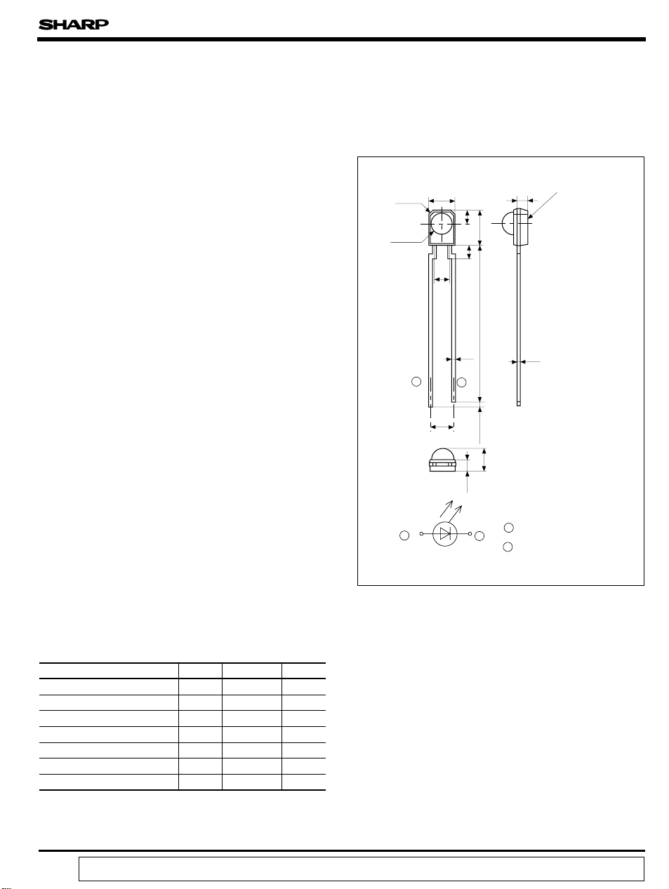
Outline Dimensions
3.0
2-C0.5
R-1.25
(1.7)
1
(2.54)
1
1.5
1.4
0.45
2
1.55
4.0
17.5
MIN0.5
2.8
2
Transparent epoxy resin
1.15
0.4
1 Anode
2 Cathode
(Unit : mm)
■
Absolute Maximum Ratings
(Ta=25˚C)
Parameter Symbol Rating Unit
Forward current
*1
Peak forward current
Reverse voltage
Power dissipation
Operating temperature
Storage temperature
*2
Soldering temperature
*1 Pulse width 100µ s, Duty ratio=0.01
*2 For MAX. 5 seconds at the position of 1.4 mm from the resin edge
“ In the absence of confirmation by device specification sheets, SHARP takes no responsibility for any defects that occur in equipment using any of SHARP's devices, shown in catalogs,
data books, etc. Contact SHARP in order to obtain the latest version of the device specification sheets before using any SHARP's device.”
I
F
I
FM
V
R
PmW
T
opr
T
stg
T
sol
50
0.5
4V
87.5
-25to+85
-40to+90
260 ˚C
mA
A
˚C
˚C
Page 2

GL496
■
Electro-optical Characteristics
Parameter Symbol Conditions MIN. TYP. MAX. Unit
Forward voltage
Peak forward voltage
Reverse current
*3
Radiant intensity
Radiant flux
Peak emission wavelength
Half intensity wavelength
Terminal capacitance
*4
Response frequency
Half intensity angle
*3 Value obtained by converting the value in power of radiant fluxes emitted at the solid angle of 0.01 sr (steradian) in the direction of mechanical axis of the lens portion
into 1 sr or all those emitted from the light emitting diode.
*4 Frequency to bring about -3dB reduction of modulated radiant intensity from 100kHz
V
F
FM
I
R
I
E
Φ IF= 50mA
E
λ
p
∆λ
Ct
fc
∆
θ
IF= 50mA
IFM= 0.5A
VR=3V
= 50mA
I
F
= 50mA
I
F
= 50mA
I
F
VR= 0V,f =1MHz
I
= 50mA +10mAp-p
F
I
= 50mA
F
-V
1.55
-V
2.6
1.75
3.6
--10µA
10.0
3.0
-
12
850
880 nm
--nm
--
--
--
±22
900
50
60
40
(Ta=25 ˚C)
-
mW/sr
-
V
mW
pF
MHz
˚
Fig. 1 Forward Current vs. Ambient
Temperature
60
50
)
40
mA
(
F
30
20
Forward current I
10
0
- 40 - 20 0 20 40 60 80 100
Ambient temperature Ta (˚C
25
)
Fig. 2 Peak Forward Current vs. Duty Ratio
-2
10
Duty ratio
Pulse width<=100 µs
Ta= 25˚C
-1
10
110
5000
)
mA
(
1000
FM
500
100
50
Peak forward current I
10
85
-4
-3
10
Page 3

GL496
Fig. 3 Spectral Distribution Fig. 4 Peak Emission Wavelength vs.
Ambient Temperature
100
80
60
40
20
Relative radiant intensity (%)
0
720 760 800 840 880 920 960 1000 1040
Wavelength λ (nm)
I F =50mA
Ta=25˚C
930
905
880
855
Peak emission wavelength λ p (nm)
830
- 25 0 25 50 75 85
Ambient temperature Ta (˚C
IF=const
)
Fig. 5 Forward Current vs. Forward Voltage Fig. 6 Relative Radiant Flux vs. Ambient
Temperature
1000
)
100
mA
(
F
10
Forward current I
Ta=75˚C
50˚C
25˚C
0˚C
-25˚C
10
1
Relative radiant flux
IF=const
1
0 0.5 1 1.5 2 2.5
Forward voltage VF (V
)
Fig. 7 Radiant Intensity vs. Forward Current
1000
)
100
mW/sr
(
E
10
DC
1
Radiant intensity I
0.1
1 10 100 1000
Forward current IF (mA
Ta=25˚C
Pulse
(pulse width <=100µs)
)
0.1
- 25 0 25 50 75 85
Ambient temperature Ta (˚C
)
Fig. 8 Relative Radiant Intensity vs. Distance
100
10
1
Relative radiant intensity (%)
0.1
0.1 1 10 100
Distance to detector (mm)
Ta=25˚C
Page 4

GL496
Fig. 9 Relative Radiant Intensity vs. Frequency
3
0
-3
-6
Relative radiant intensity (dB)
-9
0.1 1 10 40 100
Frequency f (MHz)
Fig. 11 Radiation Diagram
- 20˚ - 10˚ 0˚ 10˚ 20˚
- 30˚
- 40˚
- 50˚
- 60˚
- 70˚
- 80˚
- 90˚
Angular displacement θ
Ta=25˚C
IF=50mA+10mAp-p
T
a
= 25˚C
)
30˚
40˚
50˚
60˚
70˚
80˚
90˚
(
100
80
60
40
Relative radiant intensity (%)
20
0
Fig. 10 Relative Collector Current vs. Distance
100
10
1
Relative collector current (%)
0.1
0.1
Distance between emitter and detector d (mm)
(Detector : PT414PI)
IF=50mA
Ta=25˚C
1 10 100
●
Please refer to the chapter "Precautions for Use". (Page 78 to 93)
 Loading...