

Page 1
GL4910
GL4910
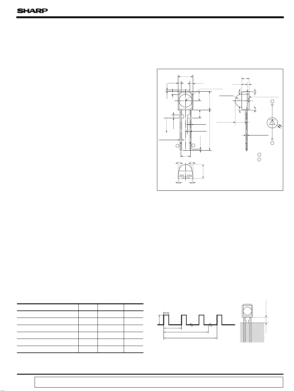
Side View Type Infrared Emitting
Diode for Camera AF
(Automatic Focusing)
± 0.2
2 - 0.4
(Unit : mm)
0.5
8˚8˚
8˚
+ 0.2
1 Cathode
2 Anode
Pink
transparent
epoxy resin
1
- 0.1
2
■■
Features
1. Small spot light diameter for easy beam diaphragming
(*Apparent emission diameter : TYP. φ 0.32 mm)
2. Uniform emission intensity on chip emitting surface
3. Low peak forward voltage type
(Peak forward voltage V
*Expansion range on lens surface of infrared emitted from chips
Applications
■
: TYP. 1.7V
FM
1. Cameras
)
Outline Dimensions
± 0.2
4.0
0.8
MAX.
Gate burrSolder dipping
0.8
0.4
0.8
range
+ 0.2
2 - 0.45
- 0.1
1
8˚
8˚
2.54
0.8
2- 0.28
2- 0.77
2
8˚
8˚
Chip center
)
2.5
(
2.15
MIN.
± 0.1
R1.75
± 0.2
5.0
(Chip position
: 2.65)
- 1.0
+ 1.5
17.15
0.3
± 0.2
3.75
* ( ) : Reference dimensions
* Tolerance : ± 0.15 mm
2.0
1.5
8˚
Absolute Maximum Ratings
■
Parameter Symbol Rating Unit
Forward current
*1
Peak forward current
Reverse voltage
Operating temperature
Storage temperature
*2
Soldering temperature
*1 30,00 cycles max. on pulse conditions shown in the right drawing
*2 For 5 seconds at the position of 2.15 mm from the resin edge
“ In the absence of confirmation by device specification sheets, SHARP takes no responsibility for any defects that occur in equipment using any of SHARP's devices, shown in catalogs,
data books, etc. Contact SHARP in order to obtain the latest version of the device specification sheets before using any SHARP's device.”
I
F
I
FM
V
T
opr
T
stg
T
sol
R
-25to+60
-40to+85
(Ta=25˚C)
50 mA
1
A
4V
˚C
˚C
260 ˚C
120 µs
FM
I
500 µs
32ms (64 pulses)
1s (1 cycle)
Soldering area
2.15mm
Page 2
GL4910
Electro-optical Characteristics
■
Parameter Symbol Conditions MIN. TYP. MAX. Unit
Forward voltage
Peak forward voltage
Reverse current
Radiant flux
Peak emission wavelength
Half intensity wavelength
Half intensity angle
Terminal capacitance
*3 Emission output to effective angle± 25˚
V
V
*3
∆λ
∆θ
(Ta=25 ˚C)
IF= 50mA
F
= 300mA, t= 10ms
I
FM
I
R
Φ
λ
C
FM
=1V
V
R
IFM= 300mA, t= 10ms
e
= 50mA
I
p
F
= 50mA
I
F
= 50mA
I
F
= 0, f= 1MH
V
t
R
Z
-
1.55
1.7 V
- 1.7 1.95 V
-- µA
4.2
850
--nm
100
9
-mW
-35-nm
- ±32 80
-
-
˚
pF
Fig. 1 Forward Current vs. Ambient Temperature Fig. 2 Peak Forward Current vs. Duty Ratio
60
50
)
mA
40
(
F
30
20
Forward current I
10
0
- 25 0 25 50 75 100 125
60
Ambient temperature Ta (˚C
)
1000
mA
(
FM
100
10
Peak forward current I
1
-4
-3
10
)
Pulse width<= 100µs
Ta= 25˚C
-2
10
Duty ratio
-1
10
110
Page 3

GL4910
Fig. 3 Spectral Distribution
100
80
60
40
20
Relative radiant intensity (%)
0
720 740 760 780 800 820 840 860 880 900 920 940 960
Wavelength λ (nm)
I =50mA
F
Ta=25˚C
Fig. 4 Peak Emission Wavelength vs.
Ambient Temperature
900
875
850
825
Peak emission wavelength λ p (nm)
800
- 25 0 25 50 75 85
Ambient temperature Ta (˚C
I =const
F
)
Fig. 5 Forward Current vs. Forward Voltage Fig. 6 Relative Radiant Flux vs. Ambient
1000
)
100
mA
(
F
10
Forward current I
50˚C
60˚C
-25˚C
0˚C
25˚C
Temperature
10
1
Relative radiant flux
I F =const
1
0 0.5
1 1.5
Forward voltage V
(V
F
2 2.5
)
0.1
-25
25 50
Ambient temperature Ta (˚C
850
75
)
Fig. 7 Radiant Flux vs. Forward Current Fig. 8 Relative Radiant Intensity vs. Distance
100
10
Radiant flux Φ e (mW)
0.1
0.01
Ta=25˚C
1
1
10
Forward current IF (mA
Pulse
(pulse width
<= 100µs)
100 1000
)
100
10
1
Relative radiant intensity (%)
0.1
0.1
1 10 100
Distance to detector (mm)
Ta=25˚C
Page 4

GL4910
Fig. 9 Radiation Diagram
- 20˚ 10˚
- 10˚ 20˚
- 30˚
- 40˚
- 50˚
- 60˚
- 70˚
- 80˚
- 90˚
100
Relative radiant intensity (%)
(
0˚
80
60
40
20
0
T
= 25˚C
a
)
30˚
40˚
50˚
60˚
70˚
80˚
90˚
Angular displacement θ
Please refer to the chapter "Precautions for Use". (Page 78 to 93)
●
 Loading...