

Page 1
GL453/GL454
GL453/GL454
Bidirectional Emission Type
Infrared Emitting Diode
■ Features
1. Bidirectional light emission type
2. High output (Φ
20mA
)
: TYP. 1.3mW at I
eF
=
3. Compact package type
4. Long lead pin type (GL454
)
5. Epoxy resin package
■ Applications
1. Light source for tape-end detectors of
VHS type VCRs
■ Absolute Maximum Ratings
Parameter Symbol Rating Unit
Power dissipation P 75 mW
Forward current I
*1
Peak forward current I
Reverse voltage V
Operating temperature T
Storage temperature T
*2
Soldering temperature T
*1 Pulse width 100µs, Duty ratio = 0.01
*2 For 3 seconds at the position of 1.8mm from the bottom face
of resin package
<=
F
FM
R
opr
stg
sol
(
Ta = 25˚C
50 mA
1A
6V
- 25 to + 85
- 40 to + 85
260 ˚C
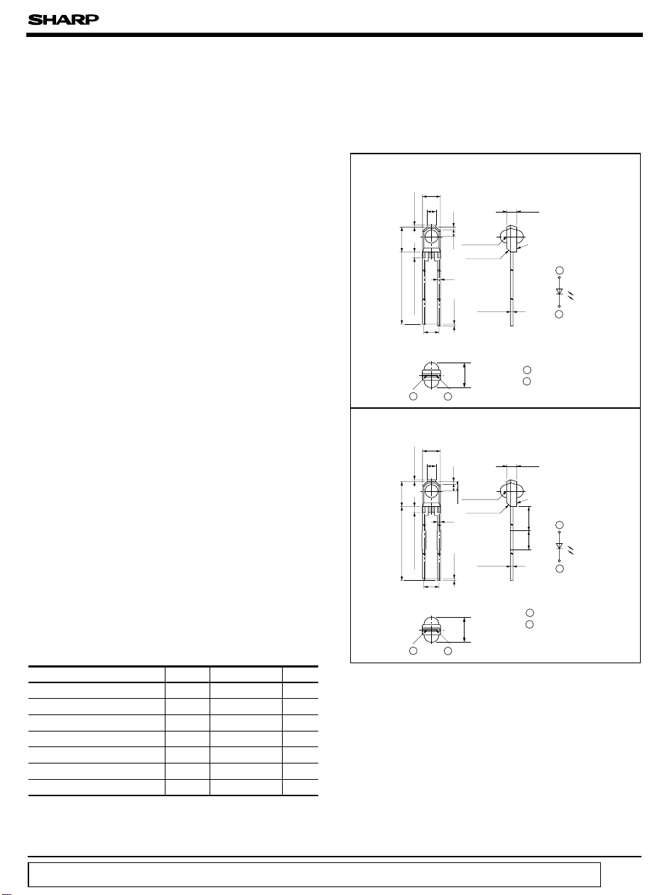
■ Outline Dimensions
GL453
MAX.
Rest of gate
± 0.2
4.2
MAX.
+ 1.5
- 1.0
18.0
GL454
MAX.
Rest of gate
± 0.2
4.2
MAX.
+ 1.5
- 1
42.0
)
± 0.2
3.0
1.5
0.3
0.51.8
2 - R1.1
C 0.65
0.5
MIN.
0.3
Resin burr 1.0
2.54
12
± 0.2
3.0
1.5
0.3
0.5
2 - R1.15
1.8
C 0.65
0.5
MIN.
0.3
Resin burr 1.0
2.54
21
2 - 0.4
4.0
2 - 0.4
4.0
± 0.2
1.7
Pink
transparent
epoxy resin
1 Anode
2 Cathode
± 0.2
1.7
Pink
transparent
epoxy resin
19
3.0
1 Anode
2 Cathode
(
Unit: mm
1
2
1
2
)
˚C
˚C
“ In the absence of confirmation by device specification sheets, SHARP takes no responsibility for any defects that occur in equipment using any of SHARP's devices, shown in catalogs,
data books, etc. Contact SHARP in order to obtain the latest version of the device specification sheets before using any SHARP's device.”
Page 2
GL453/GL454
■ Electro-optical Characteristics
Parameter Symbol Conditions MIN. TYP. MAX. Unit
Forward voltage V
Peak forward voltage V
Reverse current I
Terminal capacitance
Radiant flux
Peak emission wavelength λ
Half intensity wavelength ∆λ I
F
FM
R
C
t
Φ
e
p
(
Ta= 25˚C
IF= 20mA - 1.2 1.5 V
IFM= 0.5A - 3.0 4.0 V
VR=3V - - 10 µA
V= 0, f= 1MHz - 30 - pF
IF= 20mA 0.85 1.3 1.95 mW
IF= 5mA - 950 - nm
= 5mA - 45 - nm
F
)
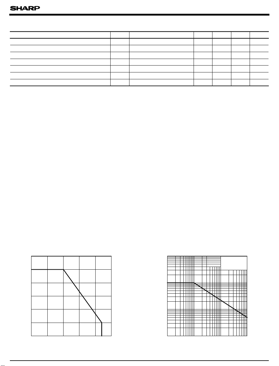
Fig. 1 Forward Current vs. Fig. 2 Peak Forward Current vs. Duty Ratio
Ambient Temperature
60
50
)
40
mA
(
F
30
20
Forward current I
10
0
-25
0 25 10050 75 85
Ambient temperature Ta (˚C
)
10000
)
mA
(
1000
FM
100
Peak forward current I
10
-3
10
10
-2
Duty ratio
-1
10
Pulse width
<=
100µs
T
= 25˚C
a
1
Page 3

GL453/GL454
Fig. 4 Peak Emission Wavelength vs.Fig. 3 Spectral Distribution
Ambient Temperature
)
nm
(
1000
975
950
I
F
= const.
100
)
80
%
(
60
40
I
= 5mA
F
Ta= 25˚C
Relative radiant intensity
20
0
880 900 940920 960 980
Wavelength λ (nm
1000 1020 1040
)
925
Peak emission wavelength λ p
900
0 25 100
-25
Ambient temperature Ta (˚C
50 75
Fig. 5 Forward Current vs. Forward Voltage Fig. 6 Relative Radiant Flux vs.
Ambient Temperature
500
T
= 75˚C
a
100
)
mA
(
F
10
Forward current I
1
0
0.4 0.8 1.2 1.6 2.0 2.4
50˚C
Forward voltage V
F
Fig. 7 Relative Radiant Flux vs.
Peak Forward Current
100
10
(V
25˚C
0˚C
25˚C
2.8
)
20
10
5
2
1
0.5
Relative radiant flux
0.2
0.1
--25
025
Ambient temperature Ta (˚C
50 75 100
Fig. 8 Relative Radiant Intensity vs.
Distance
100
)
%
(
10
)
IF= const.
)
T
= 25˚C
a
1
Relative radiant flux
0.1
10
2
10
Peak forward current IFM (mA
3
10
1
Relative radiant intensity
4
10
)
0.1
0.1 1 10 100
*Distance to detector d (mm
(
*Distance on optical axis in radiation diagram
)
)
Page 4

Fig. 9 Radiation Diagram
(
T
= 25˚C
a
60˚
50˚
40˚
30˚
(%)
20204060 40 60 8080
330˚
320˚
310˚
300˚
290˚
180˚
170˚
100
190˚
200˚
160˚
210˚
150˚
220˚
140˚
230˚
130˚
120˚
240˚
110˚ 100˚ 90˚ 80˚ 70˚
Relative radiant
intensity
270˚ 280˚
260˚
250˚
Angular displacement θ
● Please refer to the chapter “ Precautions for Use.”
20˚
340˚
)
10˚
100
350˚
GL453/GL454
90˚
1
0˚
180˚
2
270˚
0˚
1 Anode
2 Cathode
 Loading...