

Page 1
1
GL3276A
Waveform
shaper
Initial
Description
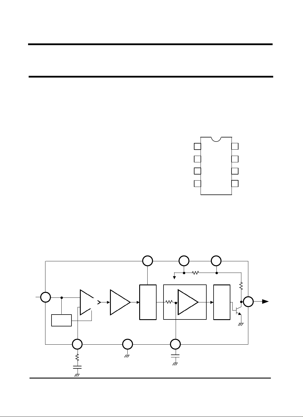
The GL3276A is a bipolar analog ICs specifically
developed for use in infrared remote control system
receiving preamplifiers. Capable of accepting a
photodiode directly, these ICs house a high gain
initial amplifier, a limiter, a band-pass filter, a
detection circuit and a waveform shaping circuit
assembled on a single chip.
Features
• Less changes of malfunction associated with
a high-frequency lighting fluorscent lamp
internal trap circuit.
• The central frequency can be varied with an
external resistance:
fo=30 to 80KHz
fo rimming reduce central frequency variance.
• Few external parts.
Internal pull-up resistance and power filter
resistance.
Lower-capacitance external capacitor
• Open collector output
Open collector output with a pull-up resistance.
Block Diagram
IN+
20
Stage
ABLC
IN-
7 5 20
R
1
C
1
Limiter
GND
Pin configuration
V
CC1
Out
V
CC2
fo
4 3 1
f
0
BPF
TRAP
Detector
+
C
D
V
C
2
R
(SOP)
1
2
3
4
CC2
S
GL3276A
GL3276A
IN+
8
IN-
7
CD 6
GND
5
V
CC1
R
L
OUT
2
OUTPUT
Page 2
2
GL3276A
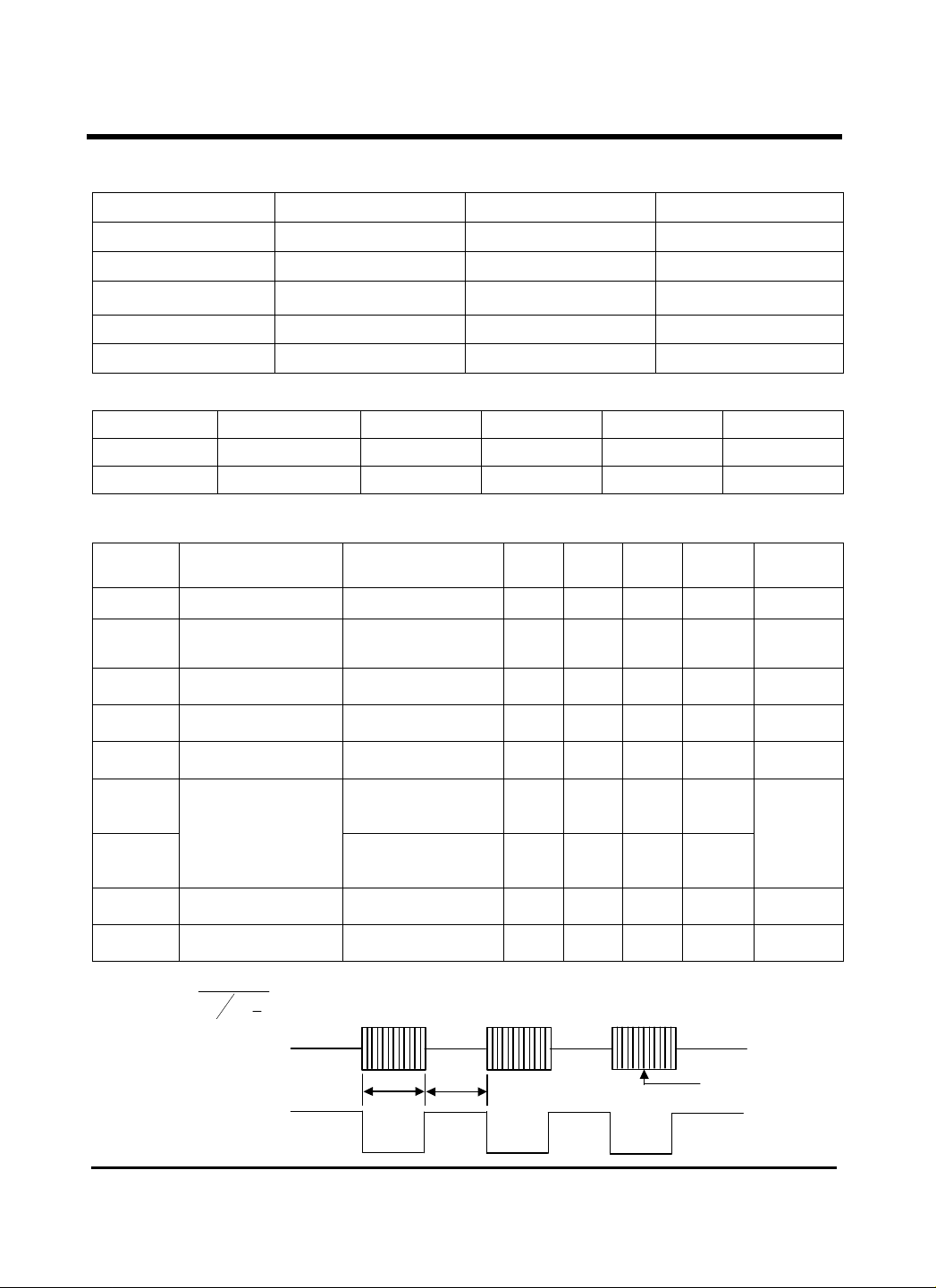
Absolute Maximum Ratings(Ta=25
¡É)
SYMBOL PARAMETER VALUE UNIT
VCC Supply voltage 6.0 V
I
Output Current 2.5 mA
OUT
PD
T
Operating temperature
OPR
T
Storage temperature -40 to +125 ¡É
STG
Allowable power
dissipation
270 mW
- 20 to +75 ¡É
Recommended Operating Condition
SYMBOL PARAMETER
VCC Supply voltage 4.5 5.0 5.5 V
fIN Input frequency
Electrical characteristics (VCC = 5.0V, Ta = 2.5
SYMBOL PARAMETER TEST CONDITION MIN TYP MAX UNIT REMARK
ICC Supply current 1.2 2.8 mA
VIN Input voltage
AV Voltage gain
FBW BPF bandwidth
rIN Input impedance
t
PW1
t
PW2
VOL
VOH
Note 1 : rIN =
Output pulse width
Low Level
output voltage
Low Level
output voltage
47
V
IN
(
X
K§Ù(where VIN=input level, VX=test value)
1)V
MIN TYP MAX UNIT
30 38 80 KHz
¡É)
IIN = 0A
IIN=-330 µA
fIN=38kHz
VIN=30 µV
P-P
-3dB Bandwidth
VIN=30 µV
P-P
fIN=38kHz CW
VIN=0.2 µV
P-P
2.0
0.6
70 76 80 dB
2.0 2.5 3.0 KHz
80 110 160 K§Ù note * 1
2.5
0.8
3.1
V
1.7
fIN=38kHz
burstwave
VIN=500 µV
P-P
440 770 µS
fIN=38kHz
burstwave
VIN=50mV
P-P
440 770 µS
0.2 0.4 V
4.8 5.0 V
note * 1
2 : input burst
wave form
output pulse
600 µS
600 µS
38KHz Carrier
Page 3
3
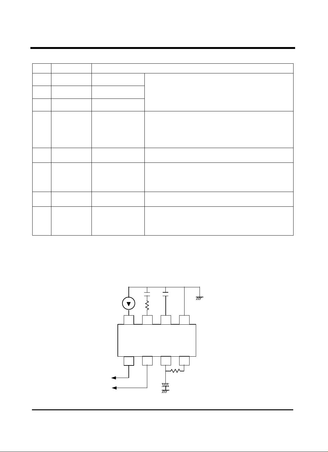
Pin Description
As the power is output to pin 3 through the internal
for easy
IN + IN - CD GND
2
6 5
C1R1
NO. SYMBOL PIN FUNCTION
GL3276A
1 V
3 V
Power input
CC1
Power output
CC2
5 GND Ground
8 IN + Input
7 IN -
Initial amplifier
Gain setup
BPF
4 fo
6 CD
2 OUT Output
frequency
setup
Detection
capacitor
Sample Application Circuits
8 Pin Plastic
SOP
• Apply a voltage of 5V ¡¾ 10 % to pin 1.
power filter resistance, connect an electrolytic
capacitor to pin 3.
• With an internal impedance of 110 K§Ù (typ.) pin 8
can accept a PIN photodiode directly. An automatic
bias level control (ABLC) circuit prevents the input
from being saturated by external light,
assuring bias level stability for the input pin.
• Initial amplifier differential inverted output. Its gain
can be set up with an external impedance.
• The central frequency of the band-pass filter can be
varied with an external resistance. A built-in trap
circuit prevents malfunctions associated with a high frequency lighting fluorescent lamp.
• Pin to which a detection capacitor is connected.
• Open collector output with pull-up resistance.
Its capability to drive a CMOS or TTL makes
connection with a receiving microcomputer.
The GL3276A has an active low output.
Photo diode
V
Power
supply
Output
8
7
GL3276A
OUT V
CC1
1
1500pF
0 to 1k
0.01µF
f0
CC2
3
130 k§Ù(R2)
47 µF
4
Page 4
4
I
CC
Supply Current
V
Voltage Gain
Vi=30¥ìVp-p
A
Voltage Gain
82
f
o
- Frequency
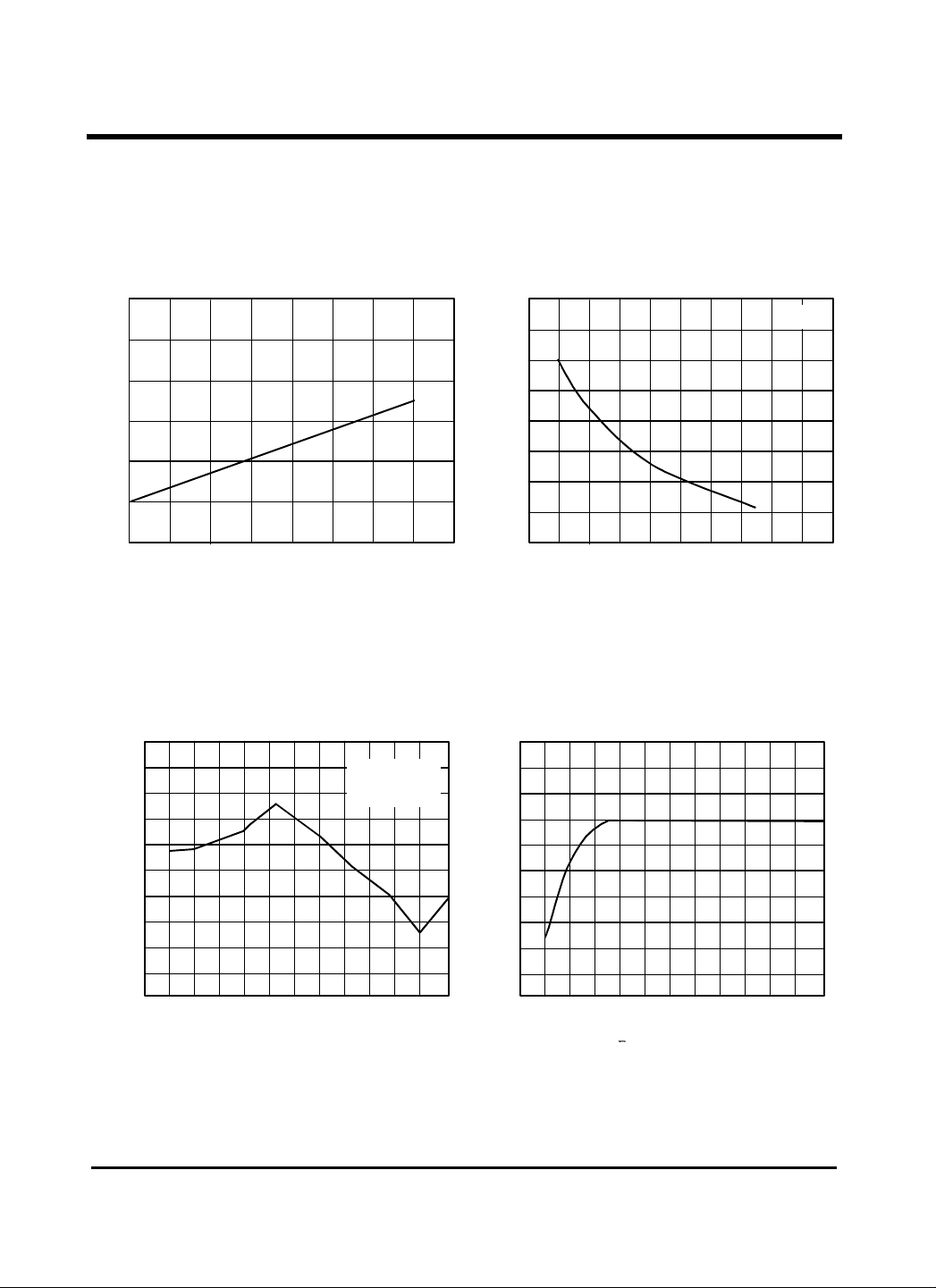
Typical Characteristics (TA = 25¡É)
2.5
-mA
2
1.5
-
1
0.5
2.5 3 3.5 4 4.5 5 5.5 6.5
90
80
70
-dB
60
50
40
-
30
20
10
0
25 30 35 40 45 50
Supply Current vs. Supply Voltage
VCC-Supply Voltage
Voltage Gain vs. Input Frequency
VCC=5V
R2=130k§Ù
fIN-Input Frequency
Frequency vs. Resistance (R2)
90
80
70
-kHz
60
50
40
30
20
40 60 80 100 120 140 160 180 200
R2-Resistance-k§Ù
Gain vs. Capacitance(C1)
78
-dB
74
70
-
V
66
1000 2000 3000 4000 5000
CI-Capacitance-pF
GL3276A
Vcc=5V
 Loading...