

Page 1
© 2000 National Semiconductor Corporation www.national.com
Geode™ GXm Processor Integrated x86 Solution with MMX Support
April 2000
Geode™ GXm Processor
Integrated x86 Solution with MMX Support
General Description
The National Semiconductor®Geode™ GXm processor
is an advanced 32-bit x86 compatible processor offering
high performance, fully accelerated 2D graphics, a 64-bit
synchronous DRAM controller and a PCI bus controller,
all on a single chip that is compatible with Intel’s MMX
technology.
The GXm processor core is a proven design that offers
competitive CPU performance. It has integer and floating
point execution units that are based on sixth-generation
technology. The integer core contains a single, six-stage
execution pipeline and offers advanced features such as
operand forwarding, branch target buffers, and extensive
write buffering. A 16 KB write-back L1 cache is accessed
in a unique fashion that eliminates pipeline stalls to fetch
operands that hit in the cache.
In addition to the advanced CPU features, the GXm processor integrates a host of functions which are typically
implemented with external components. A full-function
graphics accelerator provides pixel processing and rendering functions.
A separate on-chip video buffer enables >30 fps MPEG1
video playback when used together with the CS5530 I/O
companion chip. Graphics and system memory accesses
are supported by a tightly-coupled synchronous DRAM
(SDRAM) memory controller.This tightly coupledmemory
subsystem eliminates the need for an external L2 cache.
The GXm processor includes Virtual System Architecture
®
(VSA™ technology) enabling XpressGRAPHICS
and XpressAUDIO subsystems as well as generic emulation capabilities. Softwarehandler routines forthe XpressGRAPHICS and XpressAUDIO subsystems can be
included in the BIOS and provide compatible VGAand 16bit industry standard audio emulation.XpressAUDIO technologyeliminatesmuch of the hardware traditionallyassociated with audio functions.
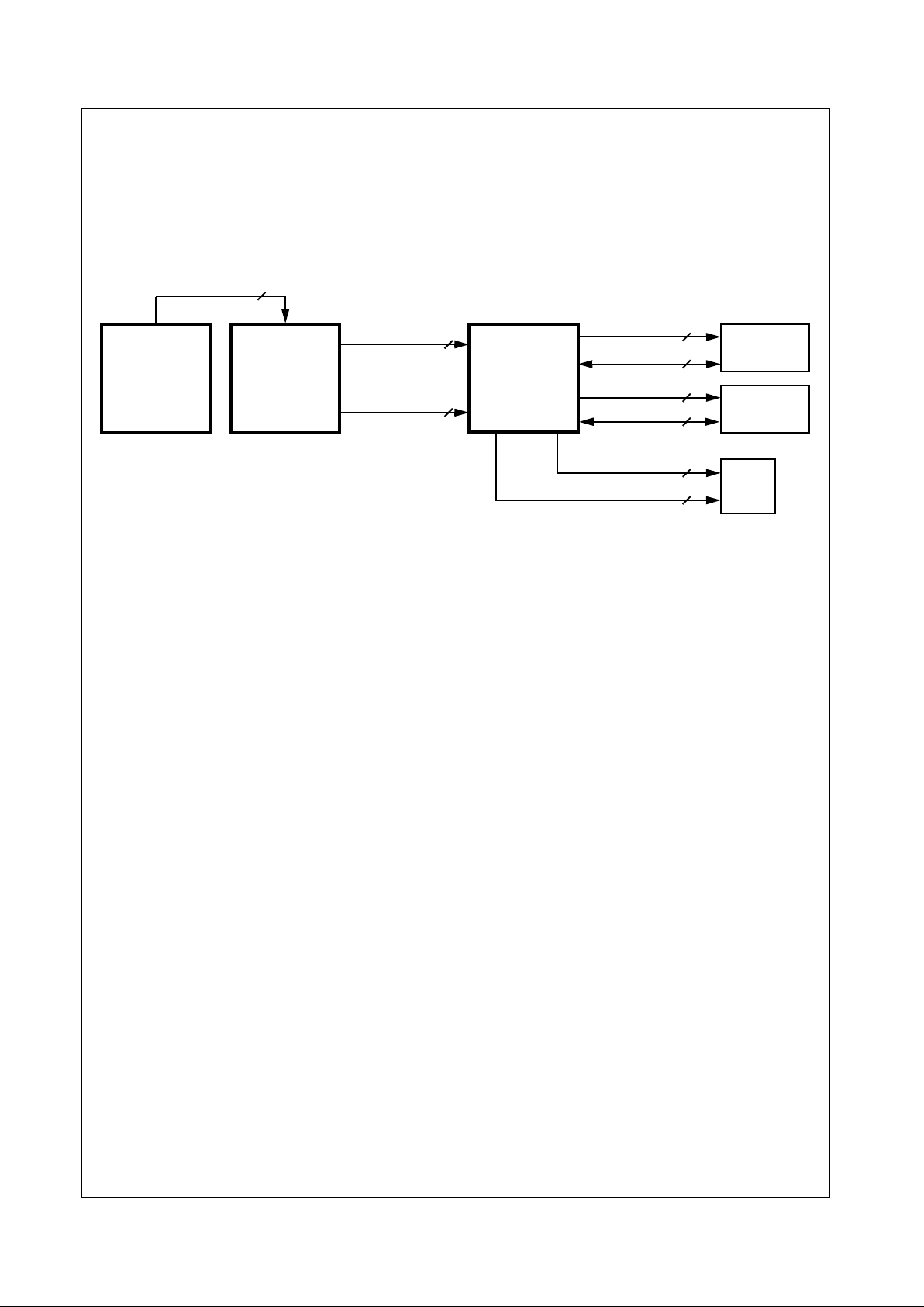
Geode™ GXm Processor Internal Block Diagram
Write-Back
Unit
FPU
Internal Bus Interface Unit
Graphics Memory Display PCI
SDRAM Port CS5530
PCI Bus
Integer
Cache Unit
Integrated
Functions
MMU
(CRT/LCD TFT)
X-Bus
Pipeline Controller Controller Controller
C-Bus
National Semiconductor and Virtual System Architecture are registered trademarks of National Semiconductor Corporation.
Geode and VSA aretrademarks of National Semiconductor Corporation.
For a complete listing of National Semiconductor trademarks, pleasevisit www.national.com/trademarks.
Page 2
www.national.com 2 Revision 3.1
Geode™ GXm Processor
Features
General Features
Packaged in:
— 352-Terminal Ball Grid Array (BGA) or
— 320-Pin Staggered Pin Grid Array (SPGA)
0.35-micron fourlayer metal CMOS process
Split rail design (3.3V I/O and 2.9V core)
32-Bit x86 Processor
Supports the MMX instruction set extension for the
acceleration of multimedia applications
Speeds offered up to 266 M Hz
16 KB unified L1 cache
Integrated Floating P oint Unit (FPU)
Re-entrant System Management Mode (SMM)
enhanced for VSA
PCI Controller
Fixed, rotating, hybrid, or ping-pong arbitration
Supports up to three PCI bus masters
Synchronous CPU and PCI bus clock frequency
Supports concurrency between PCI master andL1
cache
Power Management
Designed to support CS5530 power management
architecture
CPU only Suspend or full 3V Suspend supported:
— Clocks to CPU core stopped for CPU Suspend
— All on-chip clocks stopped for 3V Suspend
— Suspend refresh supported for 3V Suspend
Virtual Systems Architecture Technology
Architecture allows OS independent (software) virtualization of hardware functions
Provides compatiblehigh performance legacy VGA
core functionality
Note: GUI (GraphicalUser Interface) graphics accel-
eration is pure hardware.
Provides 16-bit XpressAUDIO subsystem
2D Graphics Accelerator
Graphics pipeline performance significantly increased
over previous generations by pipelining burst
reads/writes
Accelerates BitBL Ts, line draw, text
Supports all 256rasteroperations
Supports transparent BLTs
Runs at core clock frequency
Full VGA and VESA mode support
Special "Driver level”instructions utilize internal
scratchpad for enhanced performance
Display Controller
Video Generator (VG) improves memory efficiency for
display refresh with SDRAM
Supports a separate MPEG1 video buffer and data
path to enable video acceleration in the CS5530
Internal palette RAM for use with the CS5530
Direct interface to CS5530 for CRT and TFT flatpanel
support which eliminates need for external RAMDAC
Hardware frame buffer compressor/decompressor
Hardware cursor
Supports up to1280x1024x8 bpp and1024x768x16
bpp
XpressRAM Subsystem
Memory control/interface directly from CPU
64-Bit wide memory bus
Support for:
— Two 168-pin unbuffered DIMMs
— Up to 16open banks simultaneously
— Single or 16-byte reads (burst length of two)
Page 3

Revision 3.1 3 www.national.com
Table of Contents
Geode™ GXm Processor
1.0 ArchitectureOverview............................................. 8
1.1 INTEGERUNIT ...........................................................8
1.2 FLOATINGPOINTUNIT ....................................................9
1.3 WRITE-BACKCACHEUNIT .................................................9
1.4 MEMORYMANAGEMENTUNIT..............................................9
1.4.1 InternalBusInterfaceUnit ............................................9
1.5 INTEGRATED FUNCTIONS . . . . .............................................9
1.5.1 Graphics Accelerator . . . .............................................9
1.5.2 DisplayController..................................................10
1.5.3 XpressRAMMemorySubsystem ......................................10
1.5.4 PCIController.....................................................10
1.6 GEODEGXM/CS5530SYSTEMDESIGNS ....................................11
2.0 SignalDefinitions................................................ 13
2.1 PINASSIGNMENTS ......................................................13
2.2 SIGNALDESCRIPTIONS ..................................................24
2.2.1 SystemInterfaceSignals ............................................24
2.2.2 PCIInterfaceSignals ...............................................26
2.2.3 MemoryControllerInterfaceSignals ...................................29
2.2.4 VideoInterfaceSignals .............................................30
2.2.5 Power,Ground,andNoConnectSignals................................32
2.2.6 InternalTestandMeasurementSignals ................................32
2.3 SUBSYSTEMSIGNALCONNECTIONS .......................................34
2.4 POWERPLANES.........................................................36
3.0 ProcessorProgramming .......................................... 38
3.1 COREPROCESSORINITIALIZATION........................................38
3.2 INSTRUCTIONSETOVERVIEW.............................................39
3.2.1 LockPrefix .......................................................39
3.3 REGISTERSETS.........................................................40
3.3.1 ApplicationRegisterSet.............................................40
3.3.2 SystemRegisterSet ...............................................44
3.3.3 ModelSpecificRegisterSet..........................................59
3.3.4 TimeStampCounter ...............................................59
3.4 ADDRESSSPACES.......................................................60
3.4.1 I/OAddressSpace.................................................60
3.4.2 MemoryAddressSpace.............................................60
3.5 OFFSET,SEGMENT,ANDPAGINGMECHANISMS .............................61
3.6 OFFSETMECHANISM ....................................................61
3.7 DESCRIPTORSANDSEGMENTMECHANISMS................................62
3.7.1 Real and Virtual 8086 Mode Segment Mechanisms . . . . . . . . ...............62
3.7.2 SegmentMechanisminProtectiveMode................................63
3.7.3 GDTRandLDTRRegisters ..........................................66
3.7.4 DescriptorBitStructure .............................................67
3.7.5 GateDescriptors ..................................................69
3.8 MULTITASKINGANDTASKSTATESEGMENTS................................70
3.9 PAGINGMECHANISM.....................................................72
Page 4

www.national.com 4 Revision 3.1
Table of Contents (Continued)
Geode™ GXm Processor
3.10 INTERRUPTSANDEXCEPTIONS ...........................................74
3.10.1 Interrupts ........................................................74
3.10.2 Exceptions .......................................................74
3.10.3 InterruptVectors...................................................75
3.10.4 InterruptandExceptionPriorities......................................76
3.10.5 ExceptionsinRealMode ............................................77
3.10.6 ErrorCodes ......................................................77
3.11 SYSTEMMANAGEMENTMODE ............................................78
3.11.1 SMMEnhancements ...............................................79
3.11.2 SMMOperation ...................................................79
3.11.3 TheSMI#Pin .....................................................80
3.11.4 SMMConfigurationRegisters ........................................80
3.11.5 SMMMemorySpaceHeader.........................................80
3.11.6 SMMInstructions ..................................................82
3.11.7 SMMMemorySpace ...............................................83
3.11.8 SMIGeneration ...................................................83
3.11.9 SMIServiceRoutineExecution .......................................83
3.12 SHUTDOWNANDHALT ...................................................86
3.13 PROTECTION ...........................................................86
3.13.1 PrivilegeLevels ...................................................86
3.13.2 I/OPrivilegeLevels ................................................86
3.13.3 PrivilegeLevelTransfers ............................................87
3.13.4 InitializationandTransitiontoProtectedMode............................87
3.14 VIRTUAL8086MODE .....................................................88
3.14.1 MemoryAddressing................................................88
3.14.2 Protection........................................................88
3.14.3 Interrupt Handling . . . . . . ............................................88
3.14.4 EnteringandLeavingVirtual8086Mode................................88
3.15 FLOATINGPOINTUNITOPERATIONS .......................................89
3.15.1 FPU(FloatingPointUnit)RegisterSet..................................89
3.15.2 FPUTagWordRegister .............................................89
3.15.3 FPUStatusRegister ...............................................89
3.15.4 FPUModeControlRegister ..........................................89
4.0 Integrated Functions . . . . . . . . . . . . . . . . . . . . . . . . . . . . . . . . . . . . . . . . . . . . . 91
4.1 INTEGRATED FUNCTIONS PROGRAMMING INTERFACE . . . . . . . . ...............92
4.1.1 Graphics Control Register . . . . . . . . . . . . . . . ............................92
4.1.2 ControlRegisters ..................................................94
4.1.3 Graphics Memory . . . . . . ............................................94
4.1.4 L1CacheController ................................................95
4.1.5 DisplayDriverInstructions ...........................................98
4.1.6 CPU_READ/CPU_WRITEInstructions .................................99
4.2 INTERNALBUSINTERFACEUNIT..........................................100
4.2.1 FPUErrorSupport ................................................100
4.2.2 A20MSupport ...................................................100
4.2.3 SMIGeneration ..................................................100
4.2.4 640KBto1MBRegion ............................................100
4.2.5 InternalBusInterfaceUnitRegisters ..................................101
Page 5

Revision 3.1 5 www.national.com
Table of Contents (Continued)
Geode™ GXm Processor
4.3 MEMORYCONTROLLER .................................................103
4.3.1 MemoryArrayConfiguration ........................................104
4.3.2 MemoryOrganizations.............................................105
4.3.3 SDRAMCommands...............................................106
4.3.4 MemoryControllerRegisterDescription ...............................108
4.3.5 AddressTranslation ...............................................112
4.3.6 MemoryCycles ..................................................115
4.3.7 SDRAMInterfaceClocking..........................................118
4.4 GRAPHICSPIPELINE ....................................................120
4.4.1 BitBLT/VectorEngine ..............................................120
4.4.2 Master/SlaveRegisters ............................................121
4.4.3 PatternGeneration................................................121
4.4.4 SourceExpansion ................................................123
4.4.5 RasterOperations ................................................123
4.4.6 Graphics Pipeline Register Descriptions . . . . ...........................124
4.5 DISPLAYCONTROLLER..................................................129
4.5.1 DisplayFIFO ....................................................130
4.5.2 CompressionTechnology...........................................130
4.5.3 Motion Video Acceleration Support . . . . . . . . ...........................130
4.5.4 HardwareCursor .................................................131
4.5.5 DisplayTimingGenerator...........................................131
4.5.6 DitherandFrame-RateModulation ...................................131
4.5.7 DisplayModes ...................................................131
4.5.8 Graphics Memory Map . . ...........................................135
4.5.9 DisplayControllerRegisters.........................................136
4.5.10 MemoryOrganizationRegisters......................................144
4.5.11 TimingRegisters .................................................146
4.5.12 CursorPositionRegisters...........................................149
4.5.13 ColorRegisters ..................................................150
4.5.14 PaletteAccessRegisters ...........................................151
4.5.15 CS5530DisplayControllerInterface ..................................153
4.6 PCICONTROLLER ......................................................155
4.6.1 X-BusPCISlave..................................................155
4.6.2 X-BusPCIMaster ................................................155
4.6.3 PCIArbiter ......................................................155
4.6.4 GeneratingConfigurationCycles .....................................155
4.6.5 GeneratingSpecialCycles..........................................155
4.6.6 PCIConfigurationSpaceControlRegisters.............................156
4.6.7 PCIConfigurationSpaceRegisters ...................................157
4.6.8 PCICycles ......................................................162
5.0 VirtualSubsystemArchitecture ................................... 165
5.1 VIRTUALVGA ..........................................................165
5.1.1 TraditionalVGAHardware ..........................................165
5.2 GXMVIRTUALVGA......................................................167
5.2.1 DatapathElements................................................167
5.2.2 VideoRefresh ...................................................168
5.2.3 GXmVGAHardware ..............................................168
5.2.4 VGAVideoBIOS .................................................171
5.2.5 VirtualVGARegisterDescriptions ....................................172
Page 6

www.national.com 6 Revision 3.1
Table of Contents (Continued)
Geode™ GXm Processor
6.0 PowerManagement ............................................. 174
6.1 APMSUPPORT .........................................................174
6.2 CPUSUSPENDCOMMANDREGISTERS ....................................174
6.3 SUSPENDMODULATION .................................................174
6.4 3-VOLTSUSPENDMODE.................................................174
6.5 SUSPENDMODEANDBUSCYCLES .......................................175
6.5.1 InitiatingSuspendwithSUSP# ......................................175
6.5.2 InitiatingSuspendwithHALT ........................................176
6.5.3 RespondingtoaPCIAccessDuringSuspendMode......................177
6.5.4 Stopping the Input Clock ...........................................178
6.6 GXM PROCESSORSERIALBUS ..........................................179
6.6.1 SerialPacketTransmission .........................................179
6.7 POWERMANAGEMENTREGISTERS .......................................179
7.0 ElectricalSpecifications.......................................... 182
7.1 PARTNUMBERS........................................................182
7.2 ELECTRICALCONNECTIONS .............................................182
7.2.1 Power/GroundConnectionsandDecoupling ............................182
7.2.2 Power Sequencing the Core and I/O Voltages ...........................182
7.2.3 NC-DesignatedPins...............................................182
7.2.4 Pull-UpandPull-DownResistors .....................................182
7.2.5 UnusedInputPins ................................................182
7.3 ABSOLUTEMAXIMUMRATINGS...........................................183
7.4 OPERATINGCONDITIONS................................................184
7.5 DCCHARACTERISTICS ..................................................185
7.6 ACCHARACTERISTICS ..................................................186
8.0 PackageSpecifications .......................................... 195
8.1 THERMALCHARACTERISTICS ............................................195
8.1.1 HeatsinkConsiderations ...........................................196
8.2 MECHANICALPACKAGEOUTLINES........................................198
9.0 InstructionSet.................................................. 201
9.1 GENERALINSTRUCTIONSETFORMAT.....................................202
9.1.1 Prefix(Optional) .................................................203
9.1.2 Opcode.........................................................203
9.1.3 modandr/mByte(MemoryAddressing) ...............................205
9.1.4 regField ........................................................206
9.1.5 s-i-bByte(Scale,Indexing,Base) ....................................207
9.2 CPUIDINSTRUCTION....................................................208
9.2.1 Standard CPUID Levels . ...........................................208
9.2.2 ExtendedCPUIDLevels............................................210
9.3 PROCESSORCOREINSTRUCTIONSET ....................................212
9.4 FPUINSTRUCTIONSET..................................................224
9.5 MMXINSTRUCTIONSET .................................................229
9.6 NATIONAL S EMICONDUCTOR EXTENDED MMX INSTRUCTION SET . . . . . . . . . . . . . 234
Page 7

Revision 3.1 7 www.national.com
Table of Contents (Continued)
Geode™ GXm Processor
Appendix A Support Documentation . . . . . . . . . . . . . . . . . . . . . . . . . . . . . . . . . . . . . 236
A.1 ORDERINFORMATION ..................................................236
A.2 DATABOOKREVISIONHISTORY ..........................................236
Page 8
www.national.com 8 Revision 3.1
Geode™ GXm Processor
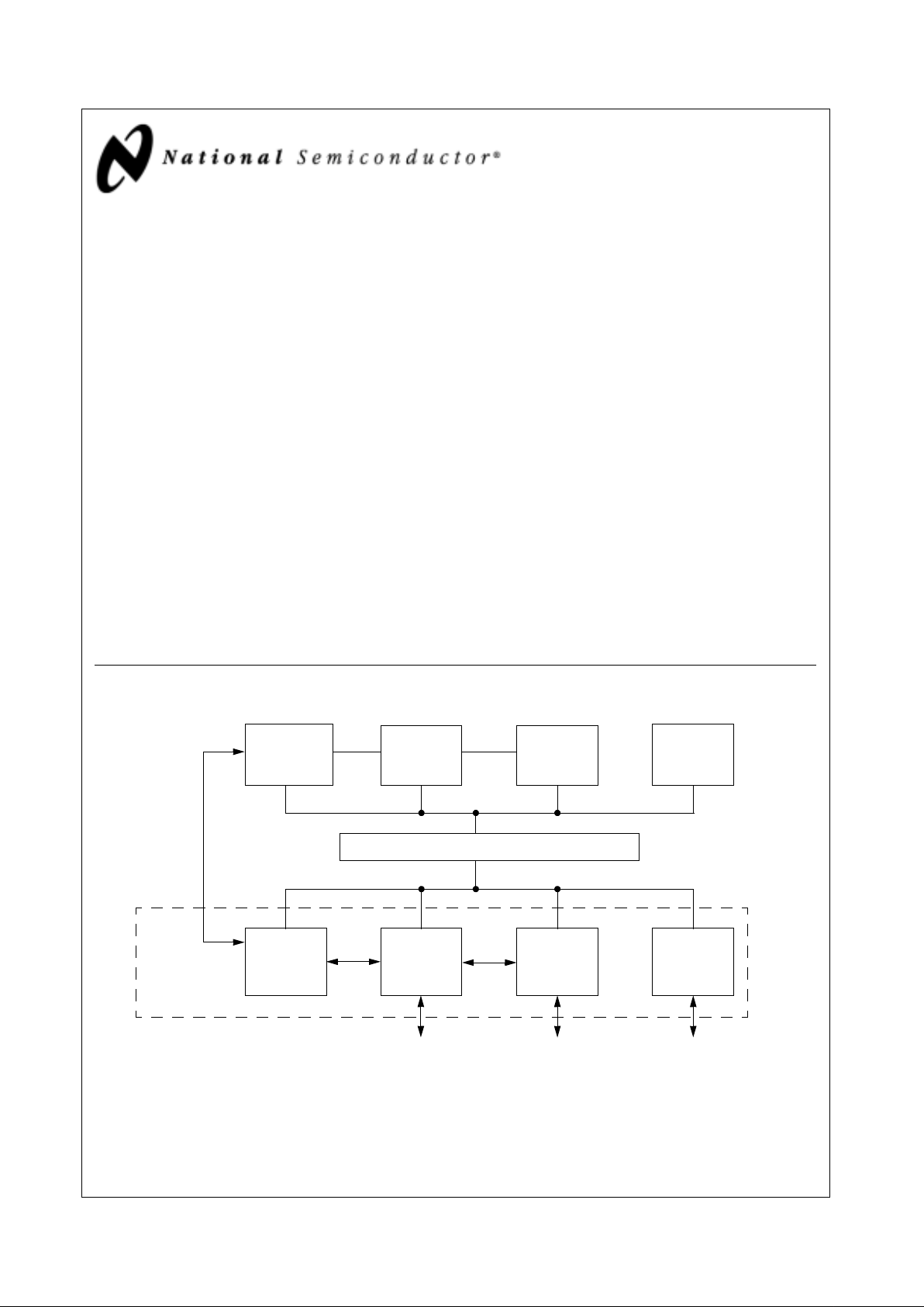
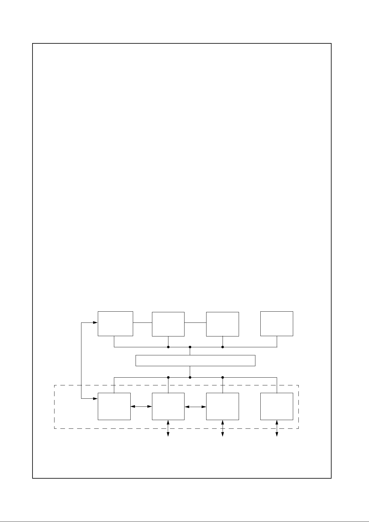
1.0 Architecture Overview
The National Semiconductor Geode GXm processor is
an x86-compatible 32-bit microprocessor. The decoupled
load/store unit (within the memory management unit)
allows multiple instructions in a single clock cycle. Other
features include single-cycle execution, single-cycle
instruction decode, 16 KB write-back cache, and clock
ratesupto266MHz.Thesefeaturesaremadepossible
by the use of advanced-process technologies and superpipelining.
The GXm processor has low power consumption at all
clock frequencies. Where additional power savings are
required, designerscanmake use of Suspend mode,Stop
Clock capability, and System Management Mode (SMM).
The GXm processor is divided into major functional blocks
(as shown in Figure 1-1):
• Integer Unit
• Floating Point Unit (FPU)
• Write-Back Cache Unit
• Memory Management Unit (MMU)
• Internal Bus Interface Unit
• IntegratedFunctions
Instructions are executed in the integer unit and in the
floating point unit. The cache unit stores the most recently
used data and instructions and provides fast access to
this information for the integer and floating point units.
1.1 INTEGER UNIT
The integer unit consists of:
• Instruction Buffer
• Instruction Fetch
• Instruction Decoder and Execution
The superpipelined integer unit fetches, decodes, and
executes x86 instructions through the use of a six-stage
integer pipeline.
The instruction fetch pipeline stage generates, from the
on-chip cache, a continuous high-speed instruction
stream for use by the processor. Up to 128 bits of code
are read during a single clock cycle.
Branch prediction logic within the prefetch unit generates
a predicted target address for unconditional or conditional
branch instructions. When a branch instruction is
detected, the instruction fetchstage starts loading instructions at the predicted address within a single clock cycle.
Up to 48 bytes of code are queued prior to the instruction
decode stage.
The instruction decode stage evaluates the code stream
provided bythe instructionfetchstageanddeterminesthe
number of bytes in each instruction and the instruction
type. Instructions are processed and decoded at a maximum rate of one instruction per clock.
The address calculation function is super-pipelined and
contains two stages, AC1 and AC2. If the instruction
refers to a memory operand, AC1 calculates a linear
memory address for the instruction.
The AC2 stage performs any required memory management functions, cache accesses, and register file
accesses. If a floating point instruction is detected by
AC2, the instruction is sent to the floating point unit for
processing.
The execution stage, under control of microcode, executes instructions using the operands provided by the
address calculation stage.
Write-back, the last stage of the integer unit, updates the
register file within the integer unit or writes to the
load/store unit within the memory managementunit.
Figure 1-1. Internal Block Diagram
Write-Back
Unit
FPU
Internal Bus Interface Unit
Graphics Memory Display PCI
SDRAM Port CS5530
PCI Bus
Integer
Cache Unit
Integrated
Functions
MMU
(CRT/LCD TFT)
X-Bus
Pipeline Controller Controller Controller
C-Bus
Page 9

Revision 3.1 9 www.national.com
Architecture Overview (Continued)
Geode™ GXm Processor
1.2 FLOATING POINT UNIT
The FPU (Floating PointUnit)interfaces to the integer unit
and the cache unit through a 64-bit bus. The FPU is x87instruction-set compatible and adheres to the IEEE-754
standard. Because almost all applications that contain
FPU instructions also contain integer instructions, the
GXm processor’s FPU achieves high performance by
completing integer and FPU operations in parallel.
FPU instructions are dispatched to the pipeline within the
integer unit. The address calculation stage of the pipeline
checks for memory management exceptions and
accesses memory operandsforusebytheFPU. Once the
instructionsandoperands havebeenprovided to the FPU,
the FPU completes instruction execution independently of
the integer unit.
1.3 WRITE-BACK CACHE UNIT
The 16 KB write-back unified cache is a data/instruction
cache and is configured as four-way set associative. The
cache stores up to 16 KB of code and data in 1024 cache
lines.
The GXm processor provides the ability to allocate a portion of the L1 cache as a scratchpad, which is used to
accelerate the Virtual Systems Architecture algorithms as
well as for some graphics operations.
1.4 MEMORY MANAGEMENT UNIT
The memory management unit (MMU) translates the linear address supplied by the integer unit into a physical
address to be used by the cache unit and the internal bus
interface unit. Memory management procedures are x86compatible, adhering to standard paging mechanisms.
The MMU also contains a load/store unit that is responsible for scheduling cache and external memory accesses.
The load/store unit incorporates two performanceenhancing features:
• Load-store reordering that gives priority to memory
reads required by the integer unit over writes to
external memory.
• Memory-read bypassing that eliminates unnecessary
memory reads by using valid data from the execution
unit.
1.4.1 Internal Bus Interface Unit
The internal bus interface unit provides a bridge from the
GXm processor to the integrated system functions (i.e.,
memory subsystem, display controller, graphics pipeline)
and the PCI bus interface.
When external memory access is required, the physical
address is calculated by the memory management unit
and then passed to the internal bus interface unit, which
translates the cycle to an X-Bus cycle (the X-Bus is a
National Semiconductor proprietary internal bus which
provides a common interface for all of the system modules). The X-Bus memory cyclenow is arbitrated between
other pending X-Bus memory requests to the SDRAM
controller before completing.
In addition, the internal bus interface unit provides configuration control for up to 20 different regions within system
memory with separate controls for read access, write
access, cacheability, and PCI access.
1.5 INTEGRATED FUNCTIONS
The GXm processor integrates the following functions traditionally implemented using external devices:
• High-performance2D graphicsaccelerator
• Separate CRT and TFT data paths from the display
controller
• SDRAM memory controller
• PCI bridge
The processor has also been enhanced to support
National Semiconductor’s proprietary Vir tual System
Architecture (VSA) implementation.
The GXm processor implements a Unified Memory Architecture (UMA). By using National Semiconductor’s Display Compression Technology (DCT), the performance
degradation inherent in traditional UMA systems is eliminated.
1.5.1 Graphics Accelerator
The graphics accelerator is a full-featured GUI (Graphical
User Interface) accelerator. The graphics pipeline implements a bitBLT engine for frame buffer bitBLTs and rectangular fills. Additional instructions in the integer unit may
be processed, as the bitBLT engine assists the CPU in the
bitBLT operations that take place between system memory and the frame buffer. This combination of hardware
and software is used by the display dr iver to provide very
fast transfers in both directions between system memory
and the frame buffer. The bitBLT engine also draws randomly-oriented vectors, and scanlines for polygon fill. All
of the pipeline operations described in the following list
can be applied to anybitBLT operation.
• Pattern Memory.Render with 8x8 dither, 8x8 monochrome, or 8x1 color pattern.
• Color Expansion. Expand monochrome bitmaps to
full-depth 8- or 16-bit colors.
• Transparency. Suppresses drawing of background
pixels for transparenttext.
• Raster Operations. Boolean operation combines
source, destination, and pattern bitmaps.
Page 10

www.national.com 10 Revision 3.1
Architecture Overview (Continued)
Geode™ GXm Processor
1.5.2 Display Controller
The display port is a direct interface to the CS5530 which
drives a TFT flat panel display, LCD panel, or a CRT display.
The display controller (video generator) retrieves image
data from the frame buffer region of memory, performs a
color-look-up if required, inserts the cursor overlay into
the pixel stream, generates display timing, and formats
the pixel data for output to a variety of display devices.
The display controller contains Display Compression
Technology (DCT) that allows the GXm processor to
refresh the display from a compressed copy of the frame
buffer. DCT typically decreases the screen-refresh bandwidth requirement by a factor of 15 to 20, further minimizing bandwidth contention.
1.5.3 XpressRAM Memory Subsystem
The memory controller drives a 64-bit SDRAM port
directly. The SDRAM memory array contains both the
main system memory and the graphicsframebuffer. Up to
four module banks of SDRAM are supported. Each module bank will have two or four component banks depending on the memory size and organization. The maximum
configuration is four module banks with four component
banks providing a total of 16 open banks. The maximum
memory size is 1 GB.
The memory controller handles multiple requests for
memory data from the GXm processor, the graphics
accelerator and the display controller. The memory controller contains extensive buffering logic that helps minimize contention for memory bandwidth between graphics
and CPU requests. The memory controller cooperates
with the internal bus controller to determine the cacheability of all memory references.
1.5.4 PCI Controller
The GXm processor incorporates a full-function PCI interface module that includes the PCI arbiter. All accesses to
external I/O devices are sent over the PCI bus, although
most memory accesses are serviced by the SDRAM controller. The Internal Bus Interface Unit contains address
mapping logic that determines if memory accesses are
targeted for the SDRAM or for the PCI bus.
Page 11
Revision 3.1 11 www.national.com
Architecture Overview (Continued)
Geode™ GXm Processor
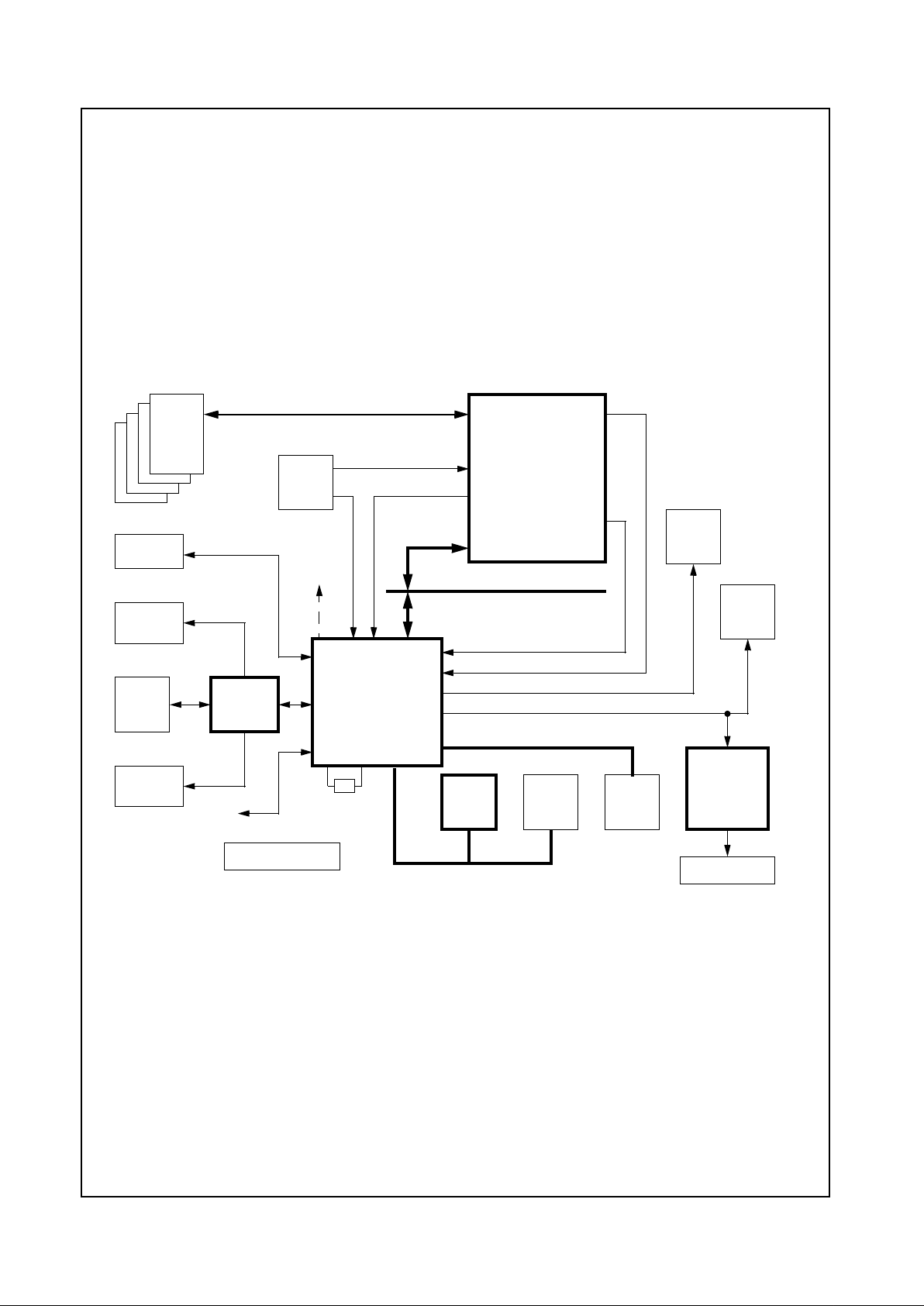
1.6 GEODE GXM/CS5530 SYSTEM DESIGNS
The GXm Integrated Subsystem with MMX support consists of two chips, the GXm Processor and the CS5530
I/O companion. The subsystem provides high performance using 32-bit x86 processing. The two chips integrate video, audio and memory interface functions
normally performed by external hardware.
As described in separate manuals, the CS5530 enables
the full features of the GXm processor with MMX support.
These features include full VGA and VESA video, 16-bit
stereo sound, IDE interface, ISA interface, SMM power
management, and AT compatibility logic. In addition, the
newer CS5530 provides an Ultra DMA/33 interface,
MPEG2 assist, and AC97 Version 2.0 compliant audio.
Figure 1-2 shows a basic block system diagram (refer to
Figure 2-4 on page 34 for detailed subsystem interconnection signals). It includes the National Semiconductor
CS9210 Dual-Scan Flat Panel Display Controller for
designs that need to interfaceto a DSTN panel (instead of
TFT panel).
Figure 1-2. Geode™ GXm/CS5530 System Block Diagram
YUV Port
(Video)
RGB Port
PCI Interface
SDRAM
MD[63:0]
PCI Bus
Geode™ CS5530
I/O Companion
Graphics Data
Video Data
Analog RGB
Digital RGB (to TFT or DSTN Panel)
CRT
TFT
Panel
USB
(2 Ports)
AC97
Codec
Speakers
CD
ROM
Audio
Microphone
GPIO
Port
(Graphics)
Super
ISA Bus
SDRAM
Serial
Packet
Clocks
I/O
BIOS
IDE
Devices
14.31818
MHz Crystal
IDE Control
System
Clocks
DC-DC & Battery
CS9210
DSTN
Controller
DSTN Panel
Geode™ GXm
Processor
Geode™
Page 12
www.national.com 12 Revision 3.1
Architecture Overview (Continued)
Geode™ GXm Processor
The CS9210 converts the digital RGB output of the
CS5530 I/O companion chip to the digital output suitable
for driving a dual-scan color STN (DSTN) flat panel LCD.
It connects to the digital RGB output of a GXm processor
or 55x0 and drives the graphics data onto a dual-scan flat
panel LCD. It can drive all standard dual-scan color STN
flat panels up to 1024x768 resolution. Figure 1-3 shows
an example of a CS9210 interface in a typical GXm Integrated Subsystem.
Figure 1-3. CS9210 Interface System Diagram
DRAM Data
Address Control
13
16
Panel Control
6
24
Panel Data
DSTN
Pixel Port
24
Pixel Data
LCD
18
CS5530
CS9210
DSTN
Controller
I/O
DRAM-B
256Kx16 Bit
DRAM-A
256Kx16 Bit
Address Control
13
DRAM Data
16
4
Serial
Configuration
Companion
(Control & Data)
Geode™ GXm
Processor
Geode™
Geode™
Page 13
Revision 3.1 13 www.national.com
Geode™ GXm Processor
2.0 Signal Definitions
This section describes the external interface of the Geode
GXm processor. Figure 2-1 shows the signals organized
by their functional interface groups (internal test and electrical pins are not shown).
2.1 PIN ASSIGNMENTS
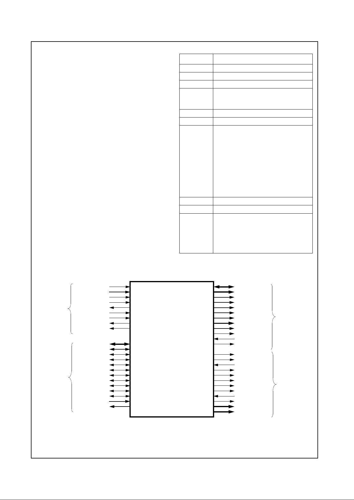
The tables in this section use several common abbreviations. Table 2-1 lists the mnemonics and their meanings.
Figure 2-2 on page 14 shows the pin assignment for the
352 BGA with Tables 2-2 and 2-3 listing the pin assignments sorted by pin number and alphabetically by signal
name, respectively.
Figure 2-3 on page 19 shows the pin assignment for the
320 SPGA with Tables 2-4 and 2-5 listing the pin assignments sorted by pin number and alphabetically by signal
name, respectively.
In Section 2.2 “Signal Descriptions” starting on Page24 a
description of each signal is provided within its associated
functional group.
Following the signal descriptions, information regarding
subsystem signal connections and split power planes and
decoupling is provided.
.
Figure 2-1. Functional Block Diagram
Table 2-1. Pin Type Definitions
Mnemonic Definition
I Standardinput pin.
I/O Bidirectional pin.
O Totem-pole output.
OD Open-drain output structure that allows
multiple devicesto share the pin in a
wired-OR configuration
PU Pull-up resistor
PD Pull-down resistor
s/t/s Sustained tri-state, an active-low tri-state
signal ownedand drivenbyoneand only
one agent at a time.The agent that
drives an s/t/s pin low must drive it high
foratleast one clockbefore lettingitfloat.
A new agent cannot start driving an s/t/s
signal any sooner than one clock after
the previous owner lets it float. A pull-up
resistor is required to sustain the inactive
state until another agent drives it, and
must be provided by the central resource.
VCC (PWR) Power pin.
VSS (GND) Ground pin
# The "#" symbol at theend of a signal
name indicates that the active, or
asserted state occurs when the signal is
at a low voltage level. When "#" is not
present after the signal name, the s ignal
is asserted when at a high voltage level.
SYSCLK
CLKMODE[2:0]
RESET
INTR
IRQ13
SMI#
SUSP#
SUSPA#
SERIALP
AD[31:0]
C/BE[3:0]#
PAR
FRAME#
IRDY#
TRDY#
STOP#
LOCK#
DEVSEL#
PERR#
SERR#
REQ[2:0]#
GNT[2:0]#
MD[63:0]
MA[12:0]
BA[1:0]
RASA#, RASB#
CASA#, CASB#
CS[3:0]#
WEA#, WEB#
DQM[7:0]
CKEA, CKEB
SDCLK[3:0]
SDCLK_IN
SDCLK_OUT
PCLK
VID_CLK
DCLK
CRT_HSYNC
CRT_VSYNC
FP_VSYNC
FP_HSYNC
ENA_DISP
VID_RDY
VID_VAL
VID_DATA[7:0]
PIXEL[17:0]
Memory
Controller
Interface
Video
Interface
Signals
PCI
Interface
Signals
System
Interface
Signals
Signals
Geode™ GXm
Processor
Page 14
www.national.com 14 Revision 3.1
Signal Definitions (Continued)
Geode™ GXm Processor
Figure 2-2. 35 2 BGA Pin Assignment Diagram
For order information refer to Section A.1 “Order Information” on page236.
1234567891011121314151617181920
21 22 23 24 25 26
A
B
C
D
E
F
G
H
J
K
L
M
N
P
R
T
U
V
W
Y
AA
AB
AC
AD
AE
AF
Index Corner
VSS VSS AD27 AD24 AD21 AD16 VCC2 FRAM#DEVS# VCC3 PERR# AD15 VSS AD11 CBE0# AD6 VCC2 AD4 AD2 VCC3 AD0 AD1 TEST2 MD2 VSS VSS
VSS VSS AD28 AD25 AD22 AD18 VCC2 CBE2#TRDY# VCC3 LOCK# PAR AD14 AD12 AD9 AD7 VCC2 INTR AD3 VCC3 TEST1 TEST3 MD1 MD33 VSS VSS
AD29 AD31 AD30 AD26 AD23 AD19 VCC2 AD17 IRDY# VCC3 STOP#SERR#CBE1# AD13 AD10 AD8 VCC2 AD5 SMI# VCC3 TEST0 IRQ13 MD32 MD34 MD3 MD35
GNT0# TDI REQ2# VSS CBE3# VSS VCC2 VSS VSS VCC3 VSS VSS VSS VSS VSS VSS VCC2 VSS VSS VCC3 VSS MD0 VSS MD4 MD36 TDN
GNT2#SUSPA#REQ0# AD20 MD6 TDP MD5 MD37
TD0 GNT1# TEST VSS VSS MD38 MD7 M D 39
VCC3 VCC3 VCC3 VCC3 VCC3 VCC3 VCC3 VCC3
TMS SUSP#REQ1# VSS VSS MD8 MD40 MD9
FPVSY TCLK RESET VSS VSS MD41 MD10 MD42
VCC2 VCC2 VCC2 VCC2 VCC2 VCC2 VCC2 VCC2
CKM1 FPHSYSERLP VSS VSS MD11 MD43 MD12
CKM2 VIDVALCKM0 VSS VSS MD44 MD13 MD45
VSS PIX1 PIX0 VSS VSS MD14 MD46 MD15
VIDCLK PIX3 PIX2 VSS VSS MD47 CASA#SYSCLK
PIX4 PIX5 PIX6 VSS VSS WEB# W EA# CASB#
PIX7 PIX8 PIX9 VSS VSS DQM0 DQM4 DQM1
VCC3 VCC3 VCC3 VCC3 VCC3 VCC3 VCC3 VCC3
PIX10 PIX11 PIX12 VSS VSS DQM5 CS2# CS0#
PIX13 CRTHS PIX14 VSS VSS RASA#RASB# MA0
VCC2 VCC2 VCC2 VCC2 VCC2 VCC2 VCC2 VCC2
PIX15 PIX16 CRTVS VSS VSS MA1 MA2 MA3
DCLK PIX17 VDAT6 VDAT7 MA4 MA5 MA6 MA7
PCLK FLT# VDAT4 VSS VOLDET VSS VCC2 VSS VSS VCC3 VSS VSS VSS VSS VSS VSS VCC2 VSS VSS VCC3 VSS DQM6 VSS MA8 MA9 MA10
VRDY VDAT5 VDAT3 VDAT0 EDISP MD63 VCC2 MD62 MD 29 VCC3 MD59 M D26 MD56 MD55 MD22 CKEB VCC2 MD51 MD18 VCC3 MD48 DQM3 CS1# MA11 BA0 BA1
VSS VSS VDAT2SCLK3 SCLK1RWCLK V CC2 SCKIN MD61 VCC3 MD28 MD58 MD25 MD24 MD 54 MD21 VCC2 M D 20 MD50 VCC3 M D 17 DQM7 CS3# MA12 VSS VSS
VSS VSS VDAT1SCLK0 SCLK2 MD31 V CC2SCKOUTMD30 VCC3 MD60 MD27 MD57 VSS MD23 MD53 VCC2 MD52 MD19 VCC3 MD49 MD16 DQM2 CKEA VSS VSS
1234567891011121314151617181920
21 22 23 24 25 26
A
B
C
D
E
F
G
H
J
K
L
M
N
P
R
T
U
V
W
Y
AA
AB
AC
AD
AE
AF
Geode™ GXm
352 BGA - Top View
Note: Signal names have been abbreviated in this figure due to space constraints.
= GND terminal
= PWR terminal (VCC2 = VCC_CORE; VCC3 = VCC_IO)
Processor
Page 15
Revision 3.1 15 www.national.com
Signal Definitions (Continued)
Geode™ GXm Processor
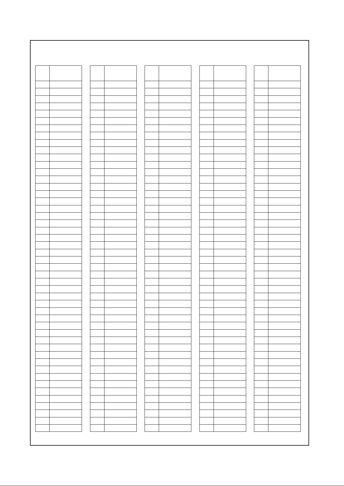
Table 2-2. 352 BGA Pin Assignments - Sorted by Pin Number
Pin
No. SignalNam e
A1 VSS
A2 VSS
A3 AD27
A4 AD24
A5 AD21
A6 AD16
A7 VCC2
A8 FRAME#
A9 DEVSEL#
A10 VCC3
A11 PERR#
A12 AD15
A13 VSS
A14 AD11
A15 C/BE0#
A16 AD6
A17 VCC2
A18 AD4
A19 AD2
A20 VCC3
A21 AD0
A22 AD1
A23 TEST2
A24 MD2
A25 VSS
A26 VSS
B1 VSS
B2 VSS
B3 AD28
B4 AD25
B5 AD22
B6 AD18
B7 VCC2
B8 C/BE2#
B9 TRD Y#
B10 VCC3
B11 LOCK#
B12 PAR
B13 AD14
B14 AD12
B15 AD9
B16 AD7
B17 VCC2
B18 INTR
B19 AD3
B20 VCC3
B21 TEST1
B22 TEST3
B23 MD1
B24 MD33
B25 VSS
B26 VSS
C1 AD29
C2 AD31
C3 AD30
C4 AD26
C5 AD23
C6 AD19
C7 VCC2
C8 AD17
C9 IRDY#
C10 VCC3
C11 STOP#
C12 SERR#
C13 C/BE1#
C14 AD13
C15 AD10
C16 AD8
C17 VCC2
C18 AD5
C19 SMI#
C20 VCC3
C21 TEST0
C22 IRQ13
C23 MD32
C24 MD34
C25 MD3
C26 MD35
D1 GNT0#
D2 TDI
D3 REQ2#
D4 VSS
D5 C/BE3#
D6 VSS
D7 VCC2
D8 VSS
D9 VSS
D10 VCC3
D11 VSS
D12 VSS
D13 VSS
D14 VSS
D15 VSS
D16 VSS
D17 VCC2
D18 VSS
Pin
No. SignalName
D19 VSS
D20 VCC3
D21 VSS
D22 MD0
D23 VSS
D24 MD4
D25 MD36
D26 TDN
E1 GNT2#
E2 SUSPA#
E3 REQ0#
E4 AD20
E23 MD6
E24 TDP
E25 MD5
E26 MD37
F1 TDO
F2 GNT1#
F3 TEST
F4 VSS
F23 VSS
F24 MD38
F25 MD7
F26 MD39
G1 VCC3
G2 VCC3
G3 VCC3
G4 VCC3
G23 VCC3
G24 VCC3
G25 VCC3
G26 VCC3
H1 TMS
H2 SUSP#
H3 REQ1#
H4 VSS
H23 VSS
H24 MD8
H25 MD40
H26 MD9
J1 FP_VSYNC
J2 TCLK
J3 RESET
J4 VSS
J23 VSS
J24 MD41
J25 MD10
J26 MD42
Pin
No. SignalName
K1 VCC2
K2 VCC2
K3 VCC2
K4 VCC2
K23 VCC2
K24 VCC2
K25 VCC2
K26 VCC2
L1 CLKMODE1
L2 FP_HSYNC
L3 SERIALP
L4 VSS
L23 VSS
L24 MD11
L25 MD43
L26 MD12
M1 CLKMODE2
M2 VID_VAL
M3 CLKMODE0
M4 VSS
M23 VSS
M24 MD44
M25 MD13
M26 MD45
N1 VSS
N2 PIXEL1
N3 PIXEL0
N4 VSS
N23 VSS
N24 MD14
N25 MD46
N26 MD15
P1 VID_CLK
P2 PIXEL3
P3 PIXEL2
P4 VSS
P23 VSS
P24 MD47
P25 CASA#
P26 SYSCLK
R1 PIXEL4
R2 PIXEL5
R3 PIXEL6
R4 VSS
R23 VSS
R24 WEB#
R25 WEA#
R26 CASB#
Pin
No. SignalN ame
T1 PIXEL7
T2 PIXEL8
T3 PIXEL9
T4 VSS
T23 VSS
T24 DQM0
T25 DQM4
T26 DQM1
U1 VCC3
U2 VCC3
U3 VCC3
U4 VCC3
U23 VCC3
U24 VCC3
U25 VCC3
U26 VCC3
V1 PIXEL10
V2 PIXEL11
V3 PIXEL12
V4 VSS
V23 VSS
V24 DQM5
V25 CS2#
V26 CS0#
W1 PIXEL13
W2 CRT_HSYNC
W3 PIXEL14
W4 VSS
W23 VSS
W24 RASA#
W25 RASB#
W26 MA0
Y1 VCC2
Y2 VCC2
Y3 VCC2
Y4 VCC2
Y23 VCC2
Y24 VCC2
Y25 VCC2
Y26 VCC2
AA1 PIXEL15
AA2 PIXEL16
AA3 CRT_VSYNC
AA4 VSS
AA23 VSS
AA24 MA1
AA25 MA2
AA26 MA3
Pin
No. SignalN ame
Page 16
www.national.com 16 Revision 3.1
Signal Definitions (Continued)
Geode™ GXm Processor
AB1 DCLK
AB2 PIXEL17
AB3 VID_DATA6
AB4 VID_DATA7
AB23 MA4
AB24 MA5
AB25 MA6
AB26 MA7
AC1 PCLK
AC2 FLT#
AC3 VID_DATA4
AC4 VSS
AC5 VOLDET
AC6 VSS
AC7 VCC2
AC8 VSS
AC9 VSS
AC10 VCC3
AC11 VSS
AC12 VSS
AC13 VSS
AC14 VSS
AC15 VSS
Pin
No. SignalNam e
AC16 VSS
AC17 VCC2
AC18 VSS
AC19 VSS
AC20 VCC3
AC21 VSS
AC22 DQM6
AC23 VSS
AC24 MA8
AC25 MA9
AC26 MA10
AD1 VID_RDY
AD2 VID_DATA5
AD3 VID_DATA3
AD4 VID_DATA0
AD5 ENA_DISP
AD6 MD63
AD7 VCC2
AD8 MD62
AD9 MD29
AD10 VCC3
AD11 MD59
AD12 MD26
Pin
No. SignalName
AD13 MD56
AD14 MD55
AD15 MD22
AD16 CKEB
AD17 VCC2
AD18 MD51
AD19 MD18
AD20 VCC3
AD21 MD48
AD22 DQM3
AD23 CS1#
AD24 MA11
AD25 BA0
AD26 BA1
AE1 VSS
AE2 VSS
AE3 VID_DATA2
AE4 SDCLK 3
AE5 SDCLK 1
AE6 RW_CLK
AE7 VCC2
AE8 SDCLK _IN
AE9 MD61
Pin
No. SignalName
AE10 VCC3
AE11 MD28
AE12 MD58
AE13 MD25
AE14 MD24
AE15 MD54
AE16 MD21
AE17 VCC2
AE18 MD20
AE19 MD50
AE20 VCC3
AE21 MD17
AE22 DQM7
AE23 CS3#
AE24 MA12
AE25 VSS
AE26 VSS
AF1 VSS
AF2 VSS
AF3 VID_DATA1
AF4 SDCLK0
AF5 SDCLK2
AF6 MD31
Pin
No. SignalN ame
AF7 VCC2
AF8 SDCLK_OUT
AF9 MD30
AF10 VCC3
AF11 MD60
AF12 MD27
AF13 MD57
AF14 VSS
AF15 MD23
AF16 MD53
AF17 VCC2
AF18 MD52
AF19 MD19
AF20 VCC3
AF21 MD49
AF22 MD16
AF23 DQM2
AF24 CKEA
AF25 VSS
AF26 VSS
Pin
No. SignalN ame
Table 2-2. 352 BGA Pin Assignments - Sorted by Pin Number (Continued)
Page 17

Revision 3.1 17 www.national.com
Signal Definitions (Continued)
Geode™ GXm Processor
Table 2-3. 352 BGA Pin Assignments - Sorted Alphabetically by Signal Name
Signal Name Type Pin No.
AD0 I/O A21
AD1 I/O A22
AD2 I/O A19
AD3 I/O B19
AD4 I/O A18
AD5 I/O C18
AD6 I/O A16
AD7 I/O B16
AD8 I/O C16
AD9 I/O B15
AD10 I/O C15
AD11 I/O A14
AD12 I/O B14
AD13 I/O C14
AD14 I/O B13
AD15 I/O A12
AD16 I/O A6
AD17 I/O C8
AD18 I/O B6
AD19 I/O C6
AD20 I/O E4
AD21 I/O A5
AD22 I/O B5
AD23 I/O C5
AD24 I/O A4
AD25 I/O B4
AD26 I/O C4
AD27 I/O A3
AD28 I/O B3
AD29 I/O C1
AD30 I/O C3
AD31 I/O C2
BA0 O AD25
BA1 O AD26
CASA# O P25
CASB# O R26
C/BE0# I/O A15
C/BE1# I/O C13
C/BE2# I/O B8
C/BE3# I/O D5
CKEA O AF24
CKEB O AD16
CLKMODE0 I M3
CLKMODE1 I L1
CLKMODE2 I M1
CRT_HSYNC O W2
CRT_VSYNC O AA3
CS0# O V26
CS1# O AD23
CS2# O V25
CS3# O AE23
DCLK I AB1
DEVSEL# s/t/s A9 (PU)
DQM0 O T24
DQM1 O T26
DQM2 O AF23
DQM3 O AD22
DQM4 O T25
DQM5 O V24
DQM6 O AC22
DQM7 O AE22
ENA_DISP O AD5
FLT# I AC2
FP_HSYNC O L2
FP_VSYNC O J1
FRAME# s/t/s A8 (PU)
GNT0# O D1
GNT1# O F2
GNT2# O E1
INTR I B18
IRDY# s/t/s C9 (PU)
IRQ13 O C22
LOCK# s/t/s B11 (PU)
MA0 O W26
MA1 O AA24
MA2 O AA25
MA3 O AA26
MA4 O AB23
MA5 O AB24
MA6 O AB25
MA7 O AB26
MA8 O AC24
MA9 O AC25
MA10 O AC26
MA11 O AD24
MA12 O AE24
MD0 I/O D22
MD1 I/O B23
MD2 I/O A24
MD3 I/O C25
MD4 I/O D24
MD5 I/O E25
MD6 I/O E23
MD7 I/O F25
MD8 I/O H24
MD9 I/O H26
MD10 I/O J25
MD11 I/O L24
MD12 I/O L26
MD13 I/O M25
MD14 I/O N24
MD15 I/O N26
MD16 I/O AF22
MD17 I/O AE21
MD18 I/O AD19
MD19 I/O AF19
Signal Name Type PinNo.
MD20 I/O AE18
MD21 I/O AE16
MD22 I/O AD15
MD23 I/O AF15
MD24 I/O AE14
MD25 I/O AE13
MD26 I/O AD12
MD27 I/O AF12
MD28 I/O AE11
MD29 I/O AD9
MD30 I/O AF9
MD31 I/O AF6
MD32 I/O C23
MD33 I/O B24
MD34 I/O C24
MD35 I/O C26
MD36 I/O D25
MD37 I/O E26
MD38 I/O F24
MD39 I/O F26
MD40 I/O H25
MD41 I/O J24
MD42 I/O J26
MD43 I/O L25
MD44 I/O M24
MD45 I/O M26
MD46 I/O N25
MD47 I/O P24
MD48 I/O AD21
MD49 I/O AF21
MD50 I/O AE19
MD51 I/O AD18
MD52 I/O AF18
MD53 I/O AF16
MD54 I/O AE15
MD55 I/O AD14
MD56 I/O AD13
MD57 I/O AF13
MD58 I/O AE12
MD59 I/O AD11
MD60 I/O AF11
MD61 I/O AE9
MD62 I/O AD8
MD63 I/O AD6
PAR I/O B12
PCLK O AC1
PERR# s/t/s A11 (PU)
PIXEL0 O N3
PIXEL1 O N2
PIXEL2 O P3
PIXEL3 O P2
PIXEL4 O R1
PIXEL5 O R2
Signal Name Type Pin No.
PIXEL6 O R3
PIXEL7 O T1
PIXEL8 O T2
PIXEL9 O T3
PIXEL10 O V1
PIXEL11 O V2
PIXEL12 O V3
PIXEL13 O W1
PIXEL14 O W3
PIXEL15 O AA1
PIXEL16 O AA2
PIXEL17 O AB2
RASA# O W24
RASB# O W25
REQ0# I E3 (PU)
REQ1# I H3 (PU)
REQ2# I D3 (PU)
RESET I J3
RW_CLK O AE6
SDCLK_IN I AE8
SDCLK_OUT O AF8
SDCLK0 O AF4
SDCLK1 O AE5
SDCLK2 O AF5
SDCLK3 O AE4
SERIALP O L3
SERR# OD C12 (PU)
SMI# I C19
STOP# s/t/s C11 (PU)
SUSP# I H2 (PU)
SUSPA# O E2
SYSCLK I P26
TCLK I J2 (PU)
TDI I D2 (PU)
TDN O D26
TDO O F1
TDP O E24
TEST I F3 (PD)
TEST0 O C21
TEST1 O B21
TEST2 O A23
TEST3 O B22
TMS I H1 (PU)
TRDY# s/t/s B9 (PU)
VCC2 PWR A7
VCC2 PWR A17
VCC2 PWR B7
VCC2 PWR B17
VCC2 PWR C7
VCC2 PWR C17
VCC2 PWR D7
VCC2 PWR D17
VCC2 PWR K1
Signal Name Type Pin No.
Page 18
www.national.com 18 Revision 3.1
Signal Definitions (Continued)
Geode™ GXm Processor
Note: PU/PD indicatespin is
internally connected to
a 20-kohm pull-up/down resistor.
VCC2 PWR K2
VCC2 PWR K3
VCC2 PWR K4
VCC2 PWR K23
VCC2 PWR K24
VCC2 PWR K25
VCC2 PWR K26
VCC2 PWR Y1
VCC2 PWR Y2
VCC2 PWR Y3
VCC2 PWR Y4
VCC2 PWR Y23
VCC2 PWR Y24
VCC2 PWR Y25
VCC2 PWR Y26
VCC2 PWR AC7
VCC2 PWR AC17
VCC2 PWR AD7
VCC2 PWR AD17
VCC2 PWR AE7
VCC2 PWR AE17
VCC2 PWR AF7
VCC2 PWR AF17
VCC3 PWR A10
VCC3 PWR A20
VCC3 PWR B10
VCC3 PWR B20
VCC3 PWR C10
VCC3 PWR C20
VCC3 PWR D10
VCC3 PWR D20
VCC3 PWR G1
VCC3 PWR G2
VCC3 PWR G3
VCC3 PWR G4
VCC3 PWR G23
VCC3 PWR G24
Signal Name Type Pin No.
VCC3 PWR G25
VCC3 PWR G26
VCC3 PWR U1
VCC3 PWR U2
VCC3 PWR U3
VCC3 PWR U4
VCC3 PWR U23
VCC3 PWR U24
VCC3 PWR U25
VCC3 PWR U26
VCC3 PWR AC10
VCC3 PWR AC20
VCC3 PWR AD10
VCC3 PWR AD20
VCC3 PWR AE10
VCC3 PWR AE20
VCC3 PWR AF10
VCC3 PWR AF20
VID_CLK O P1
VID_DATA0 O AD4
VID_DATA1 O AF3
VID_DATA2 O AE3
VID_DATA3 O AD3
VID_DATA4 O AC3
VID_DATA5 O AD2
VID_DATA6 O AB3
VID_DATA7 O AB4
VID_RDY I AD1
VID_VAL O M2
VOLDET O AC5
VSS GND A1
VSS GND A2
VSS GND A13
VSS GND A25
VSS GND A26
VSS GND B1
VSS GND B2
Signal Name Type PinNo.
VSS GND B25
VSS GND B26
VSS GND D4
VSS GND D6
VSS GND D8
VSS GND D9
VSS GND D11
VSS GND D12
VSS GND D13
VSS GND D14
VSS GND D15
VSS GND D16
VSS GND D18
VSS GND D19
VSS GND D21
VSS GND D23
VSS GND F4
VSS GND F23
VSS GND H4
VSS GND H23
VSS GND J 4
VSS GND J23
VSS GND L4
VSS GND L23
VSS GND M4
VSS GND M23
VSS GND N1
VSS GND N4
VSS GND N23
VSS GND P4
VSS GND P23
VSS GND R4
VSS GND R23
VSS GND T4
VSS GND T23
VSS GND V4
VSS GND V23
Signal Name Type Pin No.
VSS GND W4
VSS GND W23
VSS GND AA4
VSS GND AA23
VSS GND AC4
VSS GND AC6
VSS GND AC8
VSS GND AC9
VSS GND AC11
VSS GND AC12
VSS GND AC13
VSS GND AC14
VSS GND AC15
VSS GND AC16
VSS GND AC18
VSS GND AC19
VSS GND AC21
VSS GND AC23
VSS GND AE1
VSS GND AE2
VSS GND AE25
VSS GND AE26
VSS GND AF1
VSS GND AF2
VSS GND AF14
VSS GND AF25
VSS GND AF26
WEA# O R25
WEB# O R24
Signal Name Type Pin No.
Table 2-3. 352 BGA Pin Assignments - Sor ted Alphabetically by Signal Name (Continued)
Page 19
Revision 3.1 19 www.national.com
Signal Definitions (Continued)
Geode™ GXm Processor
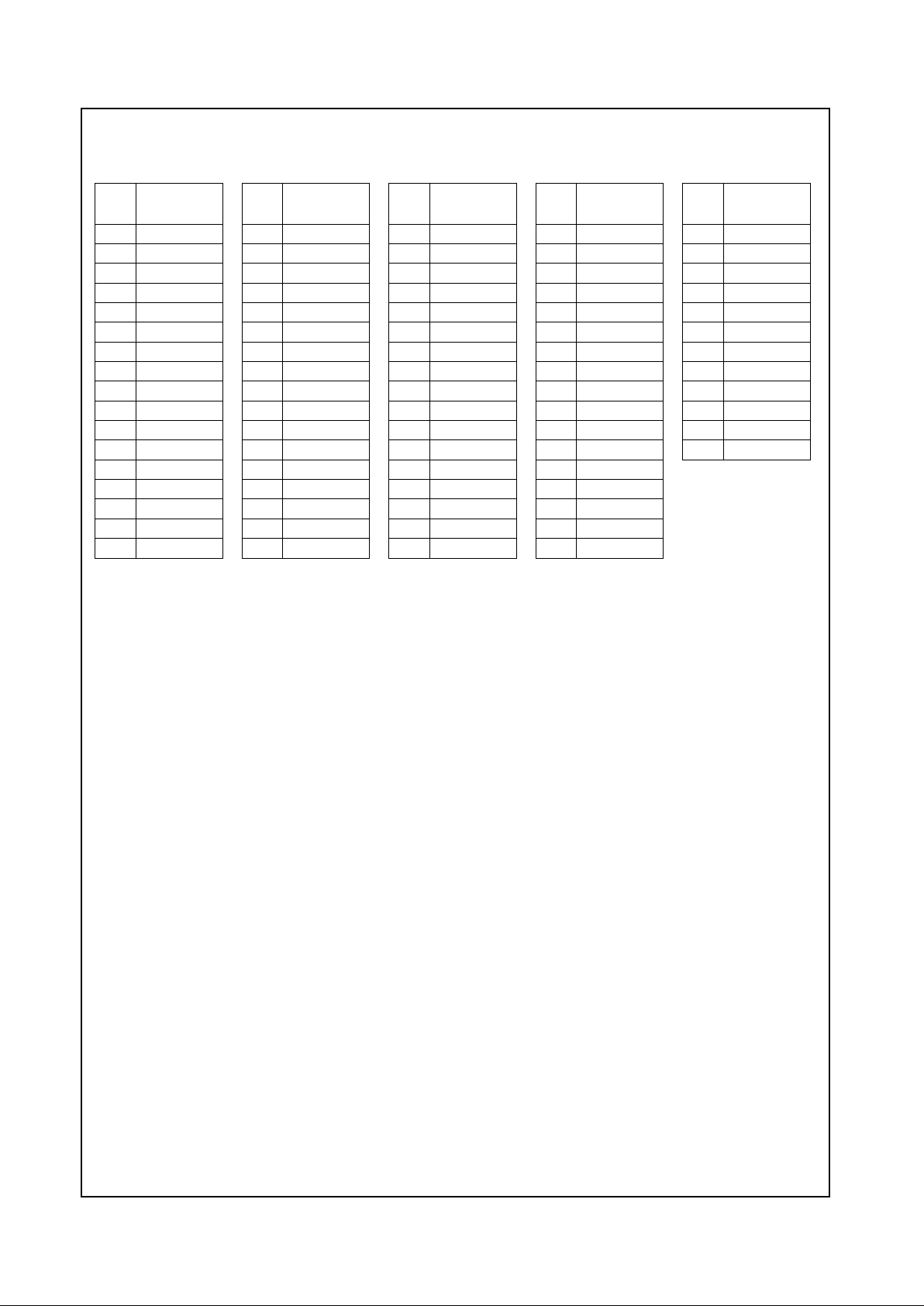
Figure 2-3. 320 SPGA Pin Assignment Diagram
For order information refer to Section A.1 “Order Information” on page236.
1234567891011121314151617181920
21 22 23 24 25 26
A
B
C
D
E
F
G
H
J
K
L
M
N
P
Q
R
S
T
U
V
AA
AB
AC
AD
AE
AF
Index Corner
27 28 29 30 31 32 33 34 35 36 37
AG
AH
AJ
AK
AL
AM
W
Y
X
Z
AN
A
B
C
D
E
F
G
H
J
K
L
M
N
P
Q
R
S
T
U
V
AA
AB
AC
AD
AE
AF
AG
AH
AJ
AK
AL
AM
W
Y
X
Z
AN
1234567891011121314151617181920
21 22 23 24 25 26 27 28 29 30 31 32 33 34 35 36 37
VCC3 AD25 VSS VCC2 AD16 VCC3 STOP# SERR# VSS AD11 AD8 VCC3 AD2 VCC2 VSS TST0 VCC3 VSS
VSS AD27 CBE3# AD21 AD19 CBE2# T RDY# LOCK# CBE1# AD13 AD9 AD6 AD3 SMI# AD1 TST2 MD33 MD2
VCC3 AD31 AD26 AD23 VCC2 AD18 FRAM E# VSS PAR VCC3 AD10 VSS AD4 AD0 VCC2 IRQ13 MD1 MD34 VCC3
AD30 AD29 AD24 AD22 AD20 AD17 IRDY# PERR# AD14 AD12 AD7 INTR TST1 TST3 MD0 MD32 MD3 MD35
REQ0# REQ2# AD28 VSS VCC2 VCC2 VSS DEVSEL# AD15 VSS CBE0# AD5 VSS VCC2 VCC2 VSS MD4 MD36 TDN
GNT0# TDI MD5 TDP
VSS CLKMODE2 VSS VSS MD37 VSS
GNT2# SUSPA#
TDO VSS TEST
REQ1# GNT1#
VCC2 VCC2 V CC2
RESET SUSP#
VCC3 TMS V SS
FPVSYN TCK
SERIALP VSS NC
CKMD1 FPHSYN
CKMD0 VID_VAL PIX0
PIX1 PIX2
VSS VCC3 VSS
PIX3 VID_CLK
PIX6 PIX5 PIX4
NC PIX9
PIX8 VSS PIX7
NC PIX10
VCC3 PIX11 VSS
PIX12 PIX13
VCC2 VCC2 V CC2
CRTHSYN DCLK
PIX14 VSS VCC2
PIX15 PIX16
VSS PIX17 VSS
CRTVSYN VDAT6
MD6 MD38
VCC2 VSS MD7
MD39 MD8
VCC2 VCC2 VCC2
MD40 MD9
VSS MD41 VCC3
MD10 MD42
MD11 VSS MD43
MD44 MD12
MD14 MD13 MD45
MD15 MD46
VSS VCC3 VSS
SYSCLK MD47
WEA# WEB# CASA#
DQM0 CASB#
DQM1 VSS DQM4
CS2# DQM5
VSS CS0# VCC3
RASB# RASA#
VCC2 VCC2 VCC2
VCC2 VSS MA1
MA2 MA0
MA4 MA3
VSS MA5 VSS
MA8 MA6MA10
PCLK FLT# VDAT5 VSS VCC2 MD31 VSS MD60 MD57 VSS MD22 MD52 VSS VCC2 VCC2 VSS BA1 MA9 MA7
VRDY VSS VDAT0 SDCLK0 SDCLK2 SDCLKIN MD29 MD27 MD56 MD55 MD21 MD20 MD50 MD16 DQM3 CS3#
VSS BA0
VCC2 VDAT4 VDAT2 SDCLK1 VCC2 RWCLKSDCLKOUT VSS MD58 VCC3 MD23 VSS MD19 MD49 VCC2 DQM6 CKEA MA11 VCC3
VDAT7 VDAT3 ENDIS SDCLK3 MD63 MD30 MD61 MD59 MD25 MD24 MD53 MD51 M D18 MD48 DQM7 DQM2 MA12 VOLDET
VSS VCC2 VDAT1 VSS VCC2 MD62 VCC3 MD28 MD26 VSS MD54 CKEB VCC3 MD17 VCC2 VSS CS1# VCC3 VSS
Note: Signal names have been abbreviated in this figure due to space constraints.
= Denotes GND terminal
= Denotes PWR terminal (VCC2 = VCC_CORE; VCC3 = VCC_IO)
320 SPGA - Top View
Processor
Geode™ GXm
Page 20
www.national.com 20 Revision 3.1
Signal Definitions (Continued)
Geode™ GXm Processor
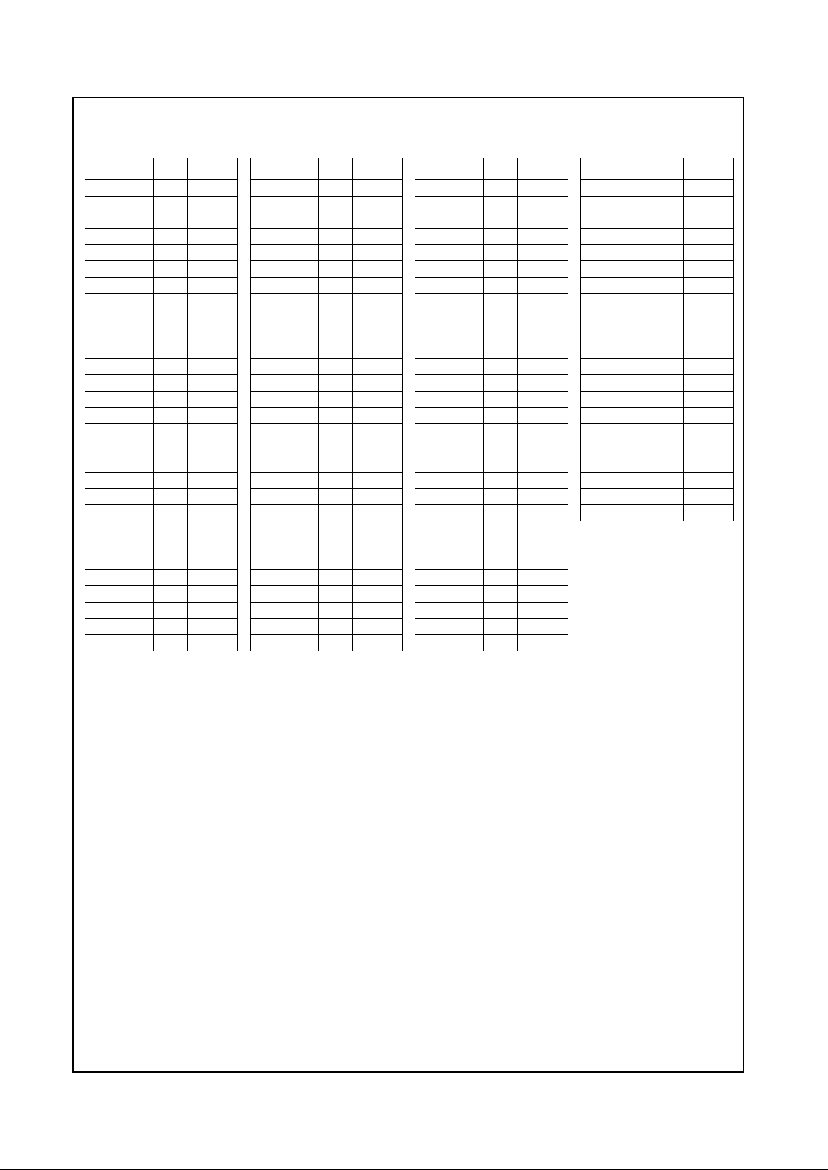
Table 2-4. 320 SPGA Pin Assignments - Sorted by Pin Number
Pin
No. Signal Name
A3 VCC3
A5 AD25
A7 VSS
A9 VCC2
A11 AD16
A13 VCC3
A15 STOP#
A17 SERR#
A19 VSS
A21 AD11
A23 AD8
A25 VCC3
A27 AD2
A29 VCC2
A31 VSS
A33 TEST0
A35 VCC3
A37 VSS
B2 VSS
B4 AD27
B6 C/BE3#
B8 AD21
B10 AD19
B12 C/BE2#
B14 TRDY#
B16 LOCK#
B18 C/BE1#
B20 AD13
B22 AD9
B24 AD6
B26 AD3
B28 SMI#
B30 AD1
B32 TEST2
B34 MD33
B36 MD2
C1 VCC3
C3 AD31
C5 AD26
C7 AD23
C9 VCC2
C11 AD18
C13 FRAME#
C15 VSS
C17 PAR
C19 VCC3
C21 AD10
C23 VSS
C25 AD4
C27 AD0
C29 VCC2
C31 IRQ13
C33 MD1
C35 MD34
C37 VCC3
D2 AD30
D4 AD29
D6 AD24
D8 AD22
D10 AD20
D12 AD17
D14 IRDY#
D16 PERR#
D18 AD14
D20 AD12
D22 AD7
D24 INTR
D26 TEST1
D28 TEST3
D30 MD0
D32 MD32
D34 MD3
D36 MD35
E1 REQ0#
E3 REQ2#
E5 AD28
E7 VSS
E9 VCC2
E11 VCC2
E13 VSS
E15 DEVSEL#
E17 AD15
E19 VSS
E21 C/BE0#
E23 AD5
E25 VSS
E27 VCC2
E29 VCC2
E31 VSS
E33 MD4
E35 MD36
E37 TDN
F2 GNT0#
F4 TDI
F34 MD5
F36 TDP
Pin
No. Signal Name
G1 VSS
G3 CLKMODE2
G5 VSS
G33 VSS
G35 MD37
G37 VSS
H2 GNT2#
H4 SUSPA#
H34 MD6
H36 MD38
J1 TDO
J3 VSS
J5 TEST
J33 VCC2
J35 VSS
J37 MD7
K2 REQ1#
K4 GNT1#
K34 MD39
K36 MD8
L1 VCC2
L3 VCC2
L5 VCC2
L33 VCC2
L35 VCC2
L37 VCC2
M2 RESET
M4 SUSP#
M34 MD40
M36 MD9
N1 VCC3
N3 TMS
N5 VSS
N33 VSS
N35 MD41
N37 VCC3
P2 FP_VSYNC
P4 TCLK
P34 MD10
P36 MD42
Q1 SERIALP
Q3 VSS
Q5 NC
Q33 MD11
Q35 VSS
Q37 MD43
R2 CLKMODE1
R4 FP_HSYNC
Pin
No. Signal Name
R34 MD44
R36 MD12
S1 CLKMODE0
S3 VID_VAL
S5 PIXEL0
S33 MD14
S35 MD13
S37 MD45
T2 PIXEL1
T4 PIXEL2
T34 MD15
T36 MD46
U1 VSS
U3 VCC3
U5 VSS
U33 VSS
U35 VCC3
U37 VSS
V2 PIXEL3
V4 VID_CLK
V34 SYSCLK
V36 MD47
W1 PIXEL6
W3 PIXEL5
W5 PIXEL4
W33 WEA#
W35 WEB#
W37 CASA#
X2 NC
X4 PIXEL9
X34 DQM0
X36 CASB#
Y1 PIXEL8
Y3 VSS
Y5 PIXEL7
Y33 DQM1
Y35 VSS
Y37 DQM4
Z2 NC
Z4 PIXEL10
Z34 CS2#
Z36 DQM5
AA1 VCC3
AA3 PIXEL11
AA5 VSS
AA33 VSS
AA35 CS0#
AA37 VCC3
Pin
No. Signal Name
AB2 PIXEL12
AB4 PIXEL13
AB34 RASB#
AB36 RASA#
AC1 VCC2
AC3 VCC2
AC5 VCC2
AC33 VCC2
AC35 VCC2
AC37 VCC2
AD2 CRT_HSYNC
AD4 DCLK
AD34 MA2
AD36 MA0
AE1 PIXEL14
AE3 VSS
AE5 VCC2
AE33 VCC2
AE35 VSS
AE37 MA1
AF2 PIXEL15
AF4 PIXEL16
AF34 MA4
AF36 MA3
AG1 VSS
AG3 PIXEL17
AG5 VSS
AG33 VSS
AG35 MA5
AG37 VSS
AH2 CRT_VSYNC
AH4 VID_DATA6
AH32 MA10
AH34 MA8
AH36 MA6
AJ1 PCLK
AJ3 FTL#
AJ5 VID_DATA5
AJ7 VSS
AJ9 VCC2
AJ11 MD31
AJ13 VSS
AJ15 MD60
AJ17 MD57
AJ19 VSS
AJ21 MD22
AJ23 MD52
AJ25 VSS
Pin
No. Signal Name
Page 21
Revision 3.1 21 www.national.com
Signal Definitions (Continued)
Geode™ GXm Processor
AJ27 VCC2
AJ29 VCC2
AJ31 VSS
AJ33 BA1
AJ35 MA9
AJ37 MA7
AK2 VID_RDY
AK4 VSS
AK6 VID_DATA0
AK8 SDCLK0
AK10 SDCLK2
AK12 SDCLK_IN
AK14 MD29
AK16 MD27
AK18 MD56
AK20 MD55
AK22 MD21
Pin
No. Signal Name
AK24 MD20
AK26 MD50
AK28 MD16
AK30 DQM3
AK32 CS3#
AK34 VSS
AK36 BA0
AL1 VCC2
AL3 VID_DATA4
AL5 VID_DATA2
AL7 SDCLK1
AL9 VCC2
AL11 RW_CLK
AL13 SDCLK_OUT
AL15 VSS
AL17 MD58
AL19 VCC3
Pin
No. Signal Name
AL21 MD23
AL23 VSS
AL25 MD19
AL27 MD49
AL29 VCC2
AL31 DQM6
AL33 CKEA
AL35 MA11
AL37 VCC3
AM2 VID_DATA7
AM4 VID_DATA3
AM6 ENA_DISP
AM8 SDCLK3
AM10 MD63
AM12 MD30
AM14 MD61
AM16 MD59
Pin
No. Signal Name
AM18 MD25
AM20 MD24
AM22 MD53
AM24 MD51
AM26 MD18
AM28 MD48
AM30 DQM7
AM32 DQM2
AM34 MA12
AM36 VOLDET
AN1 VSS
AN3 VCC2
AN5 VID_DATA1
AN7 VSS
AN9 VCC2
AN11 MD62
AN13 VCC3
Pin
No. Signal Name
AN15 MD28
AN17 MD26
AN19 VSS
AN21 MD54
AN23 CKEB
AN25 VCC3
AN27 MD17
AN29 VCC2
AN31 VSS
AN33 CS1#
AN35 VCC3
AN37 VSS
Pin
No. Signal Name
Table 2-4. 320 SPGA Pin Assignments - Sorted by Pin Number (Continued)
Page 22

www.national.com 22 Revision 3.1
Signal Definitions (Continued)
Geode™ GXm Processor
Table 2-5. 320 SPGA Pin Assignments - Sorted Alphabetically by Signal Name
Signal Name Type Pin. No.
AD0 I/O C27
AD1 I/O B30
AD2 I/O A27
AD3 I/O B26
AD4 I/O C25
AD5 I/O E23
AD6 I/O B24
AD7 I/O D22
AD8 I/O A23
AD9 I/O B22
AD10 I/O C21
AD11 I/O A21
AD12 I/O D20
AD13 I/O B20
AD14 I/O D18
AD15 I/O E17
AD16 I/O A11
AD17 I/O D12
AD18 I/O C11
AD19 I/O B10
AD20 I/O D10
AD21 I/O B8
AD22 I/O D8
AD23 I/O C7
AD24 I/O D6
AD25 I/O A5
AD26 I/O C5
AD27 I/O B4
AD28 I/O E5
AD29 I/O D4
AD30 I/O D2
AD31 I/O C3
BA0 O AK36
BA1 O AJ33
CASA# O W37
CASB# O X36
C/BE0# I/O E21
C/BE1# I/O B18
C/BE2# I/O B12
C/BE3# I/O B6
CKEA O AL33
CKEB O AN23
CLKMODE0 I S1
CLKMODE1 I R2
CLKMODE2 I G3
CRT_HSYNC O AD2
CRT_VSYNC O AH2
CS0# O AA35
CS1# O AN33
CS2# O Z34
CS3# O AK32
DCLK I AD4
DEVSEL# s/t/s E15 (PU)
DQM0 O X34
DQM1 O Y33
DQM2 O AM32
DQM3 O AK30
DQM4 O Y37
DQM5 O Z36
DQM6 O AL31
DQM7 O AM30
ENA_DISP O AM6
FLT# I AJ3
FP_HSYNC O R4
FP_VSYNC O P2
FRAME# s/t/s C13 (PU)
GNT0# O F2
GNT1# O K4
GNT2# O H2
INTR I D24
IRDY# s/t/s D14 (PU)
IRQ13 O C31
LOCK# s/t/s B16 (PU)
MA0 O AD36
MA1 O AE37
MA2 O AD34
MA3 O AF36
MA4 O AF34
MA5 O AG35
MA6 O AH36
MA7 O AJ37
MA8 O AH34
MA9 O AJ35
MA10 O AH32
MA11 O AL35
MA12 O AM34
MD0 I/O D30
MD1 I/O C33
MD2 I/O B36
MD3 I/O D34
MD4 I/O E33
MD5 I/O F34
MD6 I/O H34
MD7 I/O J37
MD8 I/O K36
MD9 I/O M36
MD10 I/O P34
MD11 I/O Q33
MD12 I/O R36
MD13 I/O S35
MD14 I/O S33
MD15 I/O T34
MD16 I/O AK28
MD17 I/O AN27
MD18 I/O AM26
MD19 I/O AL25
Signal Name Type Pin. No.
MD20 I/O AK24
MD21 I/O AK22
MD22 I/O AJ21
MD23 I/O AL21
MD24 I/O AM20
MD25 I/O AM18
MD26 I/O AN17
MD27 I/O AK16
MD28 I/O AN15
MD29 I/O AK14
MD30 I/O AM12
MD31 I/O AJ11
MD32 I/O D32
MD33 I/O B34
MD34 I/O C35
MD35 I/O D36
MD36 I/O E35
MD37 I/O G35
MD38 I/O H36
MD39 I/O K34
MD40 I/O M34
MD41 I/O N35
MD42 I/O P36
MD43 I/O Q37
MD44 I/O R34
MD45 I/O S37
MD46 I/O T36
MD47 I/O V36
MD48 I/O AM28
MD49 I/O AL27
MD50 I/O AK26
MD51 I/O AM24
MD52 I/O AJ23
MD53 I/O AM22
MD54 I/O AN21
MD55 I/O AK20
MD56 I/O AK18
MD57 I/O AJ17
MD58 I/O AL17
MD59 I/O AM16
MD60 I/O AJ15
MD61 I/O AM14
MD62 I/O AN11
MD63 I/O AM10
NC Q5
NC X2
NC Z2
PAR I/O C17
PCLK O AJ1
PERR# s/t/s D16 (PU)
PIXEL0 O S5
PIXEL1 O T2
PIXEL2 O T4
Signal Name Type Pin. No.
PIXEL3 O V2
PIXEL4 O W5
PIXEL5 O W3
PIXEL6 O W1
PIXEL7 O Y5
PIXEL8 O Y1
PIXEL9 O X4
PIXEL10 O Z4
PIXEL11 O AA3
PIXEL12 O AB2
PIXEL13 O AB4
PIXEL14 O AE1
PIXEL15 O AF2
PIXEL16 O AF4
PIXEL17 O AG3
RASA# O AB36
RASB# O AB34
REQ0# I E1 (PU)
REQ1# I K2 (PU)
REQ2# I E3 (PU)
RESET I M2
RW_CLK O AL11
SDCLK_IN I AK12
SDCLK_OUT O AL13
SDCLK0 O AK8
SDCLK1 O AL7
SDCLK2 O AK10
SDCLK3 O AM8
SERIALP O Q1
SERR# OD A17 (PU)
SMI# I B28
STOP# s/t/s A15 (PU)
SUSP# I M4 (PU)
SUSPA# O H4
SYSCLK I V34
TCLK I P4 (PU)
TDI I F4 (PU)
TDN O E37
TDO O J1
TDP O F36
TEST I J5 (PD)
TEST0 O A33
TEST1 O D26
TEST2 O B32
TEST3 O D28
TMS I N3 (PU)
TRDY# s/t/s B14 (PU)
VCC2 PWR A9
VCC2 PWR A29
VCC2 PWR C9
VCC2 PWR C29
VCC2 PWR E9
VCC2 PWR E11
Signal Name Type Pin. No.
Page 23
Revision 3.1 23 www.national.com
Signal Definitions (Continued)
Geode™ GXm Processor
Note: PU/PD indicatespin is
internally connected to
a 20-kohm pull-up/
down resistor
VCC2 PWR E27
VCC2 PWR E29
VCC2 PWR J33
VCC2 PWR L1
VCC2 PWR L3
VCC2 PWR L5
VCC2 PWR L33
VCC2 PWR L35
VCC2 PWR L37
VCC2 PWR AC1
VCC2 PWR AC3
VCC2 PWR AC5
VCC2 PWR AC33
VCC2 PWR AC35
VCC2 PWR AC37
VCC2 PWR AE5
VCC2 PWR AE33
VCC2 PWR AJ9
VCC2 PWR AJ27
VCC2 PWR AJ29
VCC2 PWR AL1
VCC2 PWR AL9
VCC2 PWR AL29
VCC2 PWR AN3
VCC2 PWR AN9
VCC2 PWR AN29
VCC3 PWR A3
VCC3 PWR A13
VCC3 PWR A25
Signal Name Type Pin. No.
VCC3 PWR A35
VCC3 PWR C1
VCC3 PWR C19
VCC3 PWR C37
VCC3 PWR N1
VCC3 PWR N37
VCC3 PWR U3
VCC3 PWR U35
VCC3 PWR AA1
VCC3 PWR AA37
VCC3 PWR AL19
VCC3 PWR AL37
VCC3 PWR AN13
VCC3 PWR AN25
VCC3 PWR AN35
VID_CLK O V4
VID_DATA0 O AK6
VID_DATA1 O AN5
VID_DATA2 O AL5
VID_DATA3 O AM4
VID_DATA4 O AL3
VID_DATA5 O AJ5
VID_DATA6 O AH4
VID_DATA7 O AM2
VID_RDY I AK2
VID_VAL O S3
VOLDET O AM36
VSS GND A7
VSS GND A19
Signal Name Type Pin. No.
VSS GND A31
VSS GND A37
VSS GND B2
VSS GND C15
VSS GND C23
VSS GND E7
VSS GND E13
VSS GND E19
VSS GND E25
VSS GND E31
VSS GND G1
VSS GND G5
VSS GND G33
VSS GND G37
VSS GND J3
VSS GND J35
VSS GND N5
VSS GND N33
VSS GND Q3
VSS GND Q35
VSS GND U1
VSS GND U5
VSS GND U33
VSS GND U37
VSS GND Y3
VSS GND Y35
VSS GND AA5
VSS GND AA33
VSS GND AE3
Signal Name Type Pin. No.
VSS GND AE35
VSS GND AG1
VSS GND AG5
VSS GND AG33
VSS GND AG37
VSS GND AJ7
VSS GND AJ13
VSS GND AJ19
VSS GND AJ25
VSS GND AJ31
VSS GND AK4
VSS GND AK34
VSS GND AL15
VSS GND AL23
VSS GND AN1
VSS GND AN7
VSS GND AN19
VSS GND AN31
VSS GND AN37
WEA# O W33
WEB# O W35
Signal Name Type Pin. No.
Table 2-5. 320 SPGA Pin Assignments - Sorted Alphabetically by Signal Name (Continued)
Page 24

www.national.com 24 Revision 3.1
Signal Definitions (Continued)
Geode™ GXm Processor
2.2 SIGNAL DESCRIPTIONS
2.2.1 System Interface Signals
Signal Name
BGA
Pin No.
SPGA
Pin No. Type Description
SYSCLK P26 V34 I System Clock
System Clock runs synchronouslywiththe PCI bus.The internal
clock of the GXm processor is generated by an internal PLL
which multipliestheSYSCLKinputandcanrun up to eight times
faster. The SYSCLK to core clock multiplier is configured using
the CLKMOD[2:0] inputs.
The SYSCLK input is a fixed frequency which can only be
stopped or varied when the G Xm processoris in a full 3V Suspend. (Section 6.4 “3-Volt SuspendMode” on page 174 for
details regarding this mode.)
CLKMODE[2:0] M1,L1,M3G3,R2,
S1
I Clock Mode
Thesesignalsareusedtosetthecoreclockmultiplier.ThePCI
clock "SYSCLK" is multiplied by the value programmed by CLKMODE[2:0] to generate the GXm processor’s core clock.
CLKMODE2isvalid only forGXmprocessor revision 4.0 and up.
The value read from DIR1 (Device ID Register 1, refer to
page 51) affects the definition of the CLKMODE pins.
If DIR1 = 30h-33h then CLKMODE[1:0]:
00 = SYSCLK multiplied by 4 (Test mode only)
01 = SYSCLK multiplied by 6
10 = SYSCLK multiplied by 7
11 = SYSCLK multiplied by 5
If DIR1 = 34h-4Fh then CLKMODE[1:0]:
00 = SYSCLK multiplied by 4 (Test mode only)
01 = SYSCLK multiplied by 6
10 = SYSCLK multiplied by 7
11 = SYSCLK multiplied by 8
If DIR1 > or = 50h then CLKMODE[2:0]:
000 = SYSCLK multiplied by 4 (Test mode only)
001 = SYSCLK multiplied by 10
010 = SYSCLK multiplied by 9
011 = SYSCLK multiplied by 5
100 = SYSCLK multiplied by 4
101 = SYSCLK multiplied by 6
110 = SYSCLK multiplied by 7
111 = SYSCLK multiplied by 8
RESET J3 M2 I Reset
RESET aborts all operationsin progress and places the
GXm processor into a reset state. RESET forces the CPU and
peripheralfunctionstobeginexecutingataknownstate. All data
in the on-chip cache is invalidated.
RESET is an asynchronous input but must meet specified setup
and hold times to guarantee recognition at a particular clock
edge. This input is typically generated during the Power-OnReset sequence.
Note: Warm Reset does not require an input on the GXm pro-
cessor since the function is virtualized using SMM.
Page 25

Revision 3.1 25 www.national.com
Signal Definitions (Continued)
Geode™ GXm Processor
INTR B18 D24 I (Maskable) Interrupt Request
INTR is a level-sensitiveinputthatcauses the GXm processor to
Suspend execution of the currentinstruction stream and begin
execution of an interrupt service routine. The INTR input can be
masked through the Flags Register IF bit. (See Table3-4 on
page 43 for bit definitions.)
IRQ13 C22 C31 O Interrupt Request Level 13
IRQ13 is asserted if an on-chip floating point error occurs.
When a floating point error occurs,the GXm processor asserts
the IRQ13 pin. The floating point interrupt handler then performs
an OUT instruction to I/O address F0h or F1h. The GXmprocessor accepts either of these cycles and clearsthe IRQ13 pin.
Refer to Section 3.4.1 “I/O Address Space” on page 60 for further information on IN/OUT instructions.
SMI# C19 B28 I System Management Interrupt
SMI# is a level-sensitiveinterrupt. SMI# puts the GXm processor
into System Management Mode (SMM).
SUSP# H2
(PU)
M4
(PU)
I Suspend Request
This signal is used to request that the GXm processor enter Suspend mode. After recognition of an active SUSP# input, theprocessor completes execution of the current instruction, any
pending decoded instructions and associated bus cycles.
SUSP# is ignored following RESET# and is enabledby setting
the SUSP bit in CCR2. (See Table 16 on page 44 for CCR2 bit
definitions.)
SincetheGXmprocessor includessystemlogic functionsaswell
as the CPU core, there are specialmodesdesignedto support
the different power management states associated with APM,
ACPI, and portable designs. The part can be configured to stop
only the CPU core clocks, or all clocks. When all clocks are
stopped, the external clock can also be stopped.(See Section
6.0 “PowerManagement” onpage174 for moredetailsregarding
power management states.)
This pin is internally connected to a 20-kohm pull-up resistor.
SUSP#ispulledupwhennotactive.
SUSPA# E2 H4 O Suspend Acknowledge
Suspend Acknowledge indicates that the GXm processor has
entered low-power Suspend mode as a result of SUSP# assertion or execution of a HALTinstruction.SUSPA# is enabled by
setting the SUSP bit in CCR2. (See Table 16 on page 44 for
CCR2 bit definitions.)
The SYSCLK input may be stopped after SUSPA# has been
asserted to further reduce power consumption if the system is
configured for 3V Suspend mode. (Section 6.4 “3-VoltSuspend
Mode” on page 174 for details regarding this mode.)
SERIALP L3 Q1 O Serial Packet
Serial Packet is the singlewire serial-transmission signal to the
CS5530 chip. The clock used for this interface is the PCI clock
(SYSCLK). This interface carries packets of miscellaneous information to the chipset to be used by the VSA software handlers.
2.2.1 System Interface Signals (Continued)
Signal Name
BGA
Pin No.
SPGA
Pin No. Type Description
Page 26

www.national.com 26 Revision 3.1
Signal Definitions (Continued)
Geode™ GXm Processor
2.2.2 PCI Interface Signals
Signal Name
BGA
Pin No.
SPGA
Pin No Type Description
AD[31:0] Refer
toTable
2-3
Refer
toTable
2-5
I/O Multiplexed Address and Data
Addressesanddata are multiplexed onthesame PCI pins. Abus
transaction consists of an address phase in the cycle in which
FRAME# is asserted followed by one or more data phases. During the address phase, AD[31:0] contain a physical 32-bit
address. For I/O,this is a byte address, for configuration and
memory it is a DWORD address. During data phases, AD[7:0]
contain the least significant byte (LSB) and AD[31:24]contain
the most significant byte (MSB). Write data is stable and valid
when IRDY# is asserted and read data is stable and valid when
TRDY# is asserted. Data is transferred during those SYSCLKS
where both IRDY# and TRDY# are asserted.
C/BE[3:0]# D5,
B8,
C13,
A15
B6,
B12,
B18,
E21
I/O Multiplexed Command and Byte Enables
Bus command and byte enables are multiplexed on the same
PCI pins. During the address phase of a transactionwhen
FRAME# is active, C/BE[3:0]# define the bus command. During
the data phase C/BE[3:0]# are used as byte enables. The byte
enables are valid for the entire data phase and determinewhich
byte lanes carry meaningful data. C/BE0#appliesto byte 0
(LSB) and C/BE3# appliesto byte 3 (MSB).
The command encoding and types are listedbelow.
0000 = Interrupt Acknowledge
0001 = Special Cycle
0010 = I/O Read
0011 = I/O Write
0100 = Reserved
0101 = Reserved
0110 = Memory Read
0111 = Memory Write
1000 = Reserved
1001 = Reserved
1010 = Configuration Read
1011 = Configuration Write
1100 = Memory ReadMultiple
1101 = Dual Address Cycle (Reserved)
1110 = Memory ReadLine
1111 = Memory Write and Invalidate
PAR B12 C17 I/O Parity
Paritygeneration is required by all PCIagents:themasterdrives
PARfor addressandwrite-dataphases, the target drivesPAR for
read-data phases. Parity is even across AD[31:0] and
C/BE[3:0]#.
For address phases, PAR is stable and valid one SYSCLK after
the address phase. It has the same timing as AD[31:0] but
delayedby one SYSCLK.
For data phases, PAR is stable and valid one SYSCLK after
either IRDY# is asserted on a write transaction or after TRDY#is
asserted on a read transaction. Once PAR is valid, it remains
valid until one SYSCLK after the completion of the data phase.
(Also see PERR#.)
Page 27

Revision 3.1 27 www.national.com
Signal Definitions (Continued)
Geode™ GXm Processor
FRAME# A8
(PU)
C13
(PU)
s/t/s Frame
Cycle Frameis driven by the current master to indicate the
beginning and duration of an access. FRAME# is asserted to
indicate a bus transaction is beginning. While FRAME# is
asserted, data transfers continue. When FRAME# is deasserted,
the transaction is in the final data phase.
This pin is internally connected to a 20-kohm pull-up resistor.
IRDY# C9
(PU)
D14
(PU)
s/t/s Initiator Ready
Initiator Ready is asserted to indicate that the bus master is able
to complete the current data phaseof the transaction. IRDY# is
used in conjunction with TRDY#. A data phase is completed on
any SYSCLK in which both IRDY# and TRDY# are sampled
asserted. During a write, IRDY# indicates valid data is present
on AD[31:0]. Duringaread,itindicatesthe master is prepared to
accept data. Wait cycles are inserted until bothIRDY# and
TRDY# are asserted together.
This pin is internally connected to a 20-kohm pull-up resistor.
TRDY# B9
(PU)
B14
(PU)
s/t/s Target Ready
TRDY# is asserted to indicate that the target agent is able to
complete the current data phase of the transaction.TRDY# is
usedinconjunction withIRDY#. A data phaseiscomplete on any
SYSCLK in which both TRDY# and IRDY# are sampled
asserted. During a read, TRDY# indicates that valid data is
present on AD[31:0]. During a write, it indicates the target is prepared to accept data. Wait cycles are inserted until both IRDY#
and TRDY#are asserted together.
This pin is internally connected to a 20-kohm pull-up resistor.
STOP# C11
(PU)
A15
(PU)
s/t/s Target Stop
STOP# is asserted to indicatethat the current target is requesting the mastertostopthecurrent transaction. This signalisused
with DEVSEL# to indicateretry, disconnect or target abort. If
STOP# is sampled active while a master, FRAME# will be deasserted and the cycle stoppedwithinthree SYSCLK cycles. As an
input, STOP# can be asserted in the following cases. 1) If a PCI
master tries to access memory that has been locked by another
master. This condition is detectedif FRAME# and LOCK# are
asserted during an addressphase. 2) STOP# will also be
asserted if the PCI write buffers are full or ifapreviously buffered
cycle has not completed. 3) Finally, STOP# can be asserted on
read cycles that cross cache line boundaries. This is conditional
based upon the programming of bit 1 in PCI Control Function 2
Register. (See Table 4-37 on page 156 forprogramming details.)
This pin is internally connected to a 20-kohm pull-up resistor.
2.2.2 PCI Interface Signals (Continued)
Signal Name
BGA
Pin No.
SPGA
Pin No Type Description
Page 28

www.national.com 28 Revision 3.1
Signal Definitions (Continued)
Geode™ GXm Processor
LOCK# B11
(PU)
B16
(PU)
s/t/s Lock Operation
LOCK# indicates an atomic operation that may require multiple
transactions to complete. When LOCK# is asserted, nonexclusivetransactions may proceedtoanaddressthatisnotcurrently
locked(atleast 16 bytes must be locked). A grant to start a transaction on PCI does not guarantee control of LOCK#. Control of
LOCK# is obtained under it own protocol in conjunction with
GNT#. It is possible fordifferent agents to use PCI while a single
master retains ownership of LOCK#. The arbiter can implement
a complete system lock. In this mode, if LOCK# is active, no
other master can gain access to the systemuntil the LOCK# is
deasserted.
This pin is internally connected to a 20-kohm pull-up resistor.
DEVSEL# A9
(PU)
E15
(PU)
s/t/s Device Select
DEVSEL# indicates that the drivingdevice has decoded its
address as the target of the current access. As an input,
DEVSEL# indicates whether any device on the bus has been
selected. DEVSEL# will also be driven by any agent that has the
ability to accept cycles on a subtractive decode basis. As a master,if no DEVSEL# is detected withinand up to the subtractive
decode clock, a master abort cyclewill result expectfor special
cycles which do not expecta DEVSEL# returned.
This pin is internally connected to a 20-kohm pull-up resistor.
PERR# A11
(PU)
D16
(PU)
s/t/s Parity Error
PERR# is used for repor ting of data parity errors during all PCI
transactions except a Special Cycle. The PERR# line is driven
two SYSCLKs after the data in which the error was detected.
This is one SYSCLK after the PAR that is attached to the data.
The minimum duration of PERR# is one SYSCLK for each data
phase in which a data parity error is detected. PERR# mustbe
driven highforoneSYSCLKbefore being in TRI-STATE mode. A
target asserts PERR# onwrite cycles if it has claimed the cycle
with DEVSEL#. The masterasserts PERR# on read cycles.
This pin is internally connected to a 20-kohm pull-up resistor.
SERR# C12
(PU)
A17
(PU)
OD System Error
System Error may be asserted by any agent for repor ting errors
other than PCI parity. The intent is to have the PCI c entral agent
assert NMI to the processor. When the Parity Enable bit is set in
the Memory Controller Configuration register, SERR# will be
asserted upon detecting a parity error on read operations from
DRAM.
REQ[2:0]# D3,
H3,
E3
(PU)
E3,
K2,
E1
(PU)
I Request Lines
Request indicates to the arbiter that an agent desires use of the
bus. Each master has its own REQ# line. REQ# priorities are
based on the arbitration scheme chosen.
Each of these pins are internallyconnected to a 20-kohm pull-up
resistor.
2.2.2 PCI Interface Signals (Continued)
Signal Name
BGA
Pin No.
SPGA
Pin No Type Description
Page 29

Revision 3.1 29 www.national.com
Signal Definitions (Continued)
Geode™ GXm Processor
GNT[2:0]# E1,
F2,
D1
H2,
K4,
F2
O Grant Lines
Grant indicatesto therequesting master that it has been granted
access to the bus. Each master has its own GNT# line. GNT#
can be pulled away at any time a higher REQ#is receivedor if
the master does not begin a cycle within a minimum period of
time (16 SYSCLKs).
2.2.2 PCI Interface Signals (Continued)
Signal Name
BGA
Pin No.
SPGA
Pin No Type Description
2.2.3 Memory Controller Interface Signals
Signal Name
BGA
Pin No.
SPGA
Pin No. Type Description
Note: The memory controller interface supports two typesof memory configurations: SDRAM modules on the sys-
tem board and JEDEC DIMMconnectors. Refer to Section 4.3 “Memory Controller” on page 103 for detailed
information regarding signal connections.
MD[63:0] Refer
toTable
2-3
Refer
toTable
2-5
I/O Memory Data Bus
The data bus lines driven to/from system memory.
MA[12:0] Refer
toTable
2-3
Refer
toTable
2-5
O Memory Address Bus
The multiplexed row/column address lines driven to the system
memory.
Supports 256 Mbit SDRAM.
BA[1:0] AD26,
AD25
AJ33,
AK36
O Bank Address Bits
These bits are used to select the component bank within the
SDRAM.
CS[3:0]# AE23,
V25,
AD23,
V26
AK32,
Z34,
AN33,
AA35
O Chip Selects
The chip selects are used to select the module bank within the
system memory. Eachchipselect corresponds to a specific module bank.
If CS# is high, the bank(s) do not respond to RAS#, CAS#, WE#
until the bank is selected again.
RASA#,
RASB#
W24,
W25
AB36,
AB34
O Row Address Strobe
RAS#, CAS#, WE# and CKE are encoded to support the different SDRAM commands. RASA# is used with CS[1:0]#. RASB#
is used with CS[3:2]#.
CASA#,
CASB#
P25,
R26
W37,
X36
O Column Address Strobe
RAS#, CAS#, WE# and CKE are encoded to support the different SDRAM commands. CASA# is used with CS[1:0]#. CASB#
is used with CS[3:2]#.
WEA#,
WEB#
R25,
R24
W33,
W35
O Write Enable
RAS#, CAS#, WE# and CKE are encoded to support the different SDRAM commands. WEA# is used with CS[1:0]#. WEB# is
used with CS[3:2]#.
Page 30

www.national.com 30 Revision 3.1
Signal Definitions (Continued)
Geode™ GXm Processor
DQM[7:0] Refer
toTable
2-3
Refer
toTable
2-5
O Data Mask Control Bits
During memory read cycles, these outputs control whether the
SDRAM output buffers are driven on the MD busornot.AllDQM
signals are asserted during read cycles.
During memory write cycles, these outputs control whether or
not MD data will be written into the SDRAM.
DQM[7:0] connect directly to the DQM7-0 pins of eachconnector.
CKEA,
CKEB
AF24,
AD16
AL33,
AN23
O Clock Enable
For normal operation CKE is held high. CKE goes low during
Suspend.
SDCLK[3:0] AE4,
AF5,
AE5,
AF4
AM8,
AK10,
AL7,
AK8
O SDRAM Clocks
The SDRAM samples all the control,address, and data using
these clocks.
SDCLK_IN AE8 AK12 I SDRAM Clock Input
The GXm processor samples the memory read data on this
clock. Works in conjunction with the SDCLK_OUT signal.
SDCLK_OUT AF8 AL13 O SDRAM Clock Output
This output is routed back to SDCLK_IN. The board designer
should vary the length of the board trace to control skew
between SDCLK_IN and SDCLK.
2.2.3 Memory Controller Interface Signals (Continued)
Signal Name
BGA
Pin No.
SPGA
Pin No. Type Description
2.2.4 Video Interface Signals
Signal Name
BGA
Pin No
SPGA
Pin No Type Description
PCLK AC1 AJ1 O Pixel Port Clock
Pixel Port Clock represents the pixel dotclock or a 2x multiple of
the dotclock for some 16-bit-per-pixel modes. It determines the
data transfer rate from the GXm processor to the CS5530.
VID_CLK P1 V4 O Video Clock
Video Clock represents the video port clock to the CS5530. This
pin is only used if the Video Port is enabled.
DCLK AB1 AD4 I DOT Clock
The DCLK input is driven from the CS5530and represents the
pixel dot clock. In some cases, such as when displaying 16 BPP
data with an eight-bit-graphics pixel port, this clock will actually
be a 2x multiple of the dotclock.
CRT_HSYNC W2 AD2 O CRT Horizontal Sync
CRT Horizontal Sync establishes the line rateand horizontal
retrace interval for an attached CRT. The polarity is programmable and depends on the display mode.
Page 31

Revision 3.1 31 www.national.com
Signal Definitions (Continued)
Geode™ GXm Processor
CRT_VSYNC AA3 AH2 O CRT Vertical Sync
CRT Vertical Sync establishes the screen refresh rate and vertical retrace interval for an attached CRT. The polarity is programmable and depends on the display mode.
FP_HSYNC L2 R4 O Flat Panel Horizontal Sync
Flat Panel Horizontal Sync establishesthe line rate and horizontal retrace interval for a TFT display. Polarity is programmable
and depends on the display mode.
This signal is an input to the CS5530. The CS5530 re-drives this
signal to the flat panel.
If no flat panel is usedinthesystem,thissignal does not need to
be connected.
FP_VSYNC J1 P2 O Flat Panel Vertical Sync
Flat Panel Vertical Sync establishes the screen refresh rate and
vertical retrace interval for a TFT display. Polarity is programmable and depends on the display mode.
This signal is an input to the CS5530. The CS5530 re-drives this
signal to the flat panel.
If no flat panel is usedinthesystem,thissignal does not need to
be connected.
ENA_DISP AD5 AM6 O Display Enable
Display Enableindicates the active display portion of a scanline
to the CS5530.
In a CS5530-based system, this signalis required to be connected even if there is no TFT panel in the system.
VID_RDY AD1 AK2 I Video Ready
This input signal indicates that the video FIFOin the CS5530 is
ready to receive more data.
VID_VAL M2 S3 O Video Valid
VID_VAL qualifies valid video data to the CS5530.
VID_DATA[7:0] Refer
to
Refer
toTable
2-5
O Video Data Bus
When the Video Port is enabled, this bus drives Video (Y-U-V)
data synchronous to the VID_CLK output.
PIXEL[17:0] Refer
toTable
2-3
Refer
toTable
2-5
O Graphics Pixel Data Bus
This bus drives graphics pixel data synchronous to the PCLK
output.
2.2.4 Video Interface Signals (Continued)
Signal Name
BGA
Pin No
SPGA
Pin No Type Description
Page 32

www.national.com 32 Revision 3.1
Signal Definitions (Continued)
Geode™ GXm Processor
2.2.5 Power, Ground,and No Connect Signals
Signal Name
BGA
Pin No.
SPGA
Pin No. Type Description
VOLDET AC5 AM36 O Voltage Detect
In early schematic revisions this pin was identified as VOLDET.
However,in the production versionthispin is a "no connect" and
should be left disconnected.
VSS Refer
toTable
2-3
(Total
of 71)
Refer
toTable
2-5
(Total
of 50)
GND Ground Connection
VCC2 Refer
toTable
2-3
(Total
of 32)
Refer
toTable
2-5
(Total
of 32)
PWR 2.9V (nominal) Core Power Connection
VCC3 Refer
toTable
2-3
(Total
of 32)
Refer
toTable
2-5
(Total
of 18)
PWR 3.3V (nominal) I/O Power Connection
NC -- Q5,X2,
Z2
No Connection
A line designated as NC shouldbe left disconnected.
2.2.6 Internal Test and Measurement Signals
Signal Name
BGA
Pin No.
SPGA
Pin No. Type Description
FLT# AC2 AJ3 I Float
Float Outputs force the GXm processor to float all outputs inthe
high-impedance state and to enter a power-down state.
RW_CLK AE6 AL11 O Raw Clock
This output is the GXmprocessorclock. This debug signal can
be used to verify clock operation.
TEST[3:0] B22,
A23,
B21,
C21
D28,
B32,
D26,
A33
O SDRAM Test Outputs
These outputs are used for internal debug only.
TCLK J2
(PU)
P4
(PU)
I Test Clock
JTAG test clock.
This pin is internally connected to a 20-kohm pull-up resistor.
TDI D2
(PU)
F4
(PU)
I Test Data Input
JTAG serial test-datainput.
This pin is internally connected to a 20-kohm pull-up resistor.
TDO F1 J1 O Test Data Output
JTAG serial test-dataoutput.
Page 33

Revision 3.1 33 www.national.com
Signal Definitions (Continued)
Geode™ GXm Processor
TMS H1
(PU)
N3
(PU)
I Test Mode Select
JTAG test-mode select.
This pin is internally connected to a 20-kohm pull-up resistor.
TEST F3
(PD)
J5
(PD)
I Test
Test-modeinput.
This pin is internally connected to a 20-kohm pull-down resistor.
TDP E24 F36 O Thermal Diode Positive
TDP is the positive terminal of the thermal diode on the die. The
diode is used to do thermal characterization of the device in a
system. This signal works in conjunction with TDN.
TDN D26 E37 O Thermal Diode Negative
TDN is thenegative terminal of thethermaldiodeon the die. The
diode is used to do thermal characterization of the device in a
system. This signal works in conjunction with TDP.
2.2.6 Internal Test and Measurement Signals
Signal Name
BGA
Pin No.
SPGA
Pin No. Type Description
Page 34

www.national.com 34 Revision 3.1
Signal Definitions (Continued)
Geode™ GXm Processor
2.3 SUBSYSTEM SIGNAL CONNECTIONS
As previously stated, the GXm Integrated Subsystem with
MMX support consists of two chips: the GXm Processor
and the CS5530 I/O companion. Figure 2-4 shows the
signal connections between the processor and the I/O
companion chip.
Figure 2-4. Subsystem Signal Connections
SYSCLK
SERIALP
IRQ13
SMI#
PCLK
CRT_HSYNC
CRT_VSYNC
PIXEL[17:0]
FP_HSYNC
FP_VSYNC
ENA_DISP
VID_VAL
VID_CLK
VID_DATA[7:0]
VID_RDY
INTR
SUSP#
SUSPA#
AD[31:0]
C/BE[3:0]#
PAR
FRAME#
IRDY#
TRDY#
STOP#
LOCK#
DEVSEL#
PERR#
SERR#
REQ0#
GX_CLK
PSERIAL
IRQ13
SMI#
PCLK
HSYNC
VSYNC
PIXEL[23:0]
FP_HSYNC
FP_VSYNC
FP_ENA_DISP
VID_VAL
VID_CLK
VID_DATA[7:0]
VID_RDY
CPU_RST
INTR
SUSP#
SUSPA#
AD[31:0]
C/BE[3:0]#
PAR
FRAME#
IRDY#
TRDY#
STOP#
LOCK#
DEVSEL#
PERR#
SERR#
REQ#
GNT#GNT0#
Geode™ CS5530
I/O Companion
Exclusive
Interconnect
Signals
(Do not connect to
any other device)
Nonexclusive
Interconnect
Signals
(May also connect
to other circuitry)
Not needed if
CRT only (no TFT)
(Note)
Note: Refer toFigure 2-5 for interconnection of these lines.
RESET
DCLK DCLK
Geode™ GXm
Processor
Page 35

Revision 3.1 35 www.national.com
Signal Definitions (Continued)
Geode™ GXm Processor
Figure 2-5. PIXEL Signal Connections
PIXEL17
PIXEL16
PIXEL15
PIXEL14
PIXEL13
PIXEL12
PIXEL11
PIXEL10
PIXEL9
PIXEL8
PIXEL7
PIXEL6
PIXEL5
PIXEL4
PIXEL3
PIXEL2
PIXEL1
Geode™ CS5530
I/O Companion
PIXEL0
PIXEL23
PIXEL22
PIXEL21
PIXEL20
PIXEL19
PIXEL18
PIXEL17
PIXEL16
PIXEL15
PIXEL14
PIXEL13
PIXEL12
PIXEL11
PIXEL10
PIXEL9
PIXEL8
PIXEL7
PIXEL6
PIXEL5
PIXEL4
PIXEL3
PIXEL2
PIXEL1
PIXEL0
Geode™ GXm
Processor
Page 36

www.national.com 36 Revision 3.1
Signal Definitions (Continued)
Geode™ GXm Processor
2.4 POWER PLANES
Figure 2-6 shows layout recommendationsforsplittingthe
power plane between VCC2 (core: 2.9V) and VCC3 (I/O:
3.3V) volts in the BGA package.
The illustration assumes there is one power plane, and no
components on the back of the board
Figure 2-7 shows layout recommendations for splitting the
power plane between VCC2 (core: 2.9V) and VCC3 (I/O:
3.3V) volts for the GXm in theSPGA package.
Figure 2-6. BGA Recommended Split Power Plane and Decoupling
1
26
A
AF
AF
A
26
1
= High frequency capacitor
= 220µF, lowE SR capacitor
= 3.3V connection
= 2.9V connection
Geode™ GXm
352 BGA - Top View
2.9V Plane
(VCC2)
3.3V Plane
(VCC3)
3.3V Plane
(VCC3)
3.3V Plane
(VCC3)
2.9V Plane
(VCC2)
Legend
Processor
Page 37

Revision 3.1 37 www.national.com
Signal Definitions (Continued)
Geode™ GXm Processor
Figure 2-7. SPGA Recommended Split Power Plane and Decoupling
1 37
A
AN
A
AN
1 37
2.9V Plane
(VCC2)
3.3V Plane
(VCC3)
3.3V Plane
(VCC3)
3.3V Plane
(VCC3)
3.3V Plane
(VCC3)
2.9V Plane
(VCC2)
To 2.9V
Regulator
Note: Wheresignals cross plane splits,it is recommended toinclude AC
decoupling between planes with 47pF capacitors.
= High frequency capacitor
= 220 µF, low ESR capacitor
= 3.3V connection
= 2.9V connection
Legend
320 SPGA - Top View
Geode™ GXm
Processor
Page 38

www.national.com 38 Revision 3.1
Geode™ GXm Processor
3.0 Processor Programming
This section describes the internal operations of the
Geode GXm processor from a programmer’s point of view.
It includes a description of the traditional “core” processing and FPU operations. The integrated function registers
are described at the endof this chapter.
The primary register sets within the processor core
include:
• Application Register Set
• System Register Set
• Model Specific Register Set
• Floating Point Unit Register Set.
The initialization of the major registers within in core are
showninTable3-1.
Theintegratedfunctionsetsarelocatedinmainmemory
space and include:
• Internal Bus Interface Unit Register Set
• Graphics PipelineRegisterSet
• DisplayControllerRegister Set
• Memory Controller Register Set
• Power Management Register Set
3.1 CORE PROCESSOR INITIALIZATION
The GXm processor is initialized when the RESET signal
is asserted. The processor is placed in realmode and the
registers listed in Table 3-1 are set to their initialized values. RESET invalidates and disables the CPU cache, and
turns off paging. When RESET is asserted, the CPU terminates all local bus activity and all internal execution.
During the entire time that RESET is asserted, the internal pipeline is flushed and no instruction execution or bus
activity occurs.
Approximately 150 to 250 external clock cycles after
RESET is deasserted, the processor begins executing
instructions at the top of physical memory (address location FFFFFFF0h). The actual time depends on the clock
scaling in use. Also, an additional 2
20
clock cycles are
needed when self-test is requested.
Typically, an intersegment jump is placed at FFFFFFF0h.
This instruction will force the processor to begin execution
in the lowest 1 MB of address space.
Thefollowingtable,Table3-1,liststhecoreregistersand
illustrates how they are initialized.
Ta ble 3-1. Initialized Core Register Controls
Register Register Name Initialized Contents Comments
EAX Accumulator xxxxxxxxh 00000000h indicates self-test passed.
EBX Base xxxxxxxxh
ECX Count xxxxxxxxh
EDX Data xxxx 04 [DIR0]h DIR0 = Device ID
EBP Base Pointer xxxxxxxxh
ESI Source Index xxxxxxxxh
EDI Destination Index xxxxxxxxh
ESP Stack Pointer xxxxxxxxh
EFLAGS Extended FLAGS 00000002h See Table 3-4 on page 43 for bit definitions.
EIP Instruction Pointer 0000FFF0h
ES Extra Segment 0000h Base address set to 00000000h. Limit set to FFFFh.
CS Code Segment F000h Base address set to FFFF0000h. Limit set to FFFFh.
SS Stack Segment 0000h Base address set to 00000000h. Limit set to FFFFh.
DS Data Segment 0000h Base address set to 00000000h. Limit set to FFFFh.
FS Extra Segment 0000h Base address set to 00000000h. Limit set to FFFFh.
GS ExtraSegment 0000h Base address set to 00000000h. Limit set to FFFFh.
IDTR Interrupt Descriptor Table Register Base = 0, Limit = 3FFh
GDTR Global Descriptor Table Register xxxx xxxxh
LDTR Local Descriptor Table Register xxxxh
TR Task Register xxxxh
CR0 Machine Status Word 60000010h See Table 3-7 on page 49 for bit definitions.
CR2 Control Register 2 xxxxxxxxh See Table3-7 on page 49 for bit definitions.
CR3 Control Register 3 xxxxxxxxh See Table3-7 on page 49 for bit definitions.
CR4 Control Register 4 00000000h See Table 3-7 on page 49 for bit definitions.
CCR1 Configuration Control 1 00h See Table 3-11 on page 49 forbit definitions.
CCR2 Configuration Control 2 00h See Table 3-11 on page 49 forbit definitions.
CCR3 Configuration Control 3 00h See Table 3-11 on page 49 forbit definitions.
CCR7 Configuration Control 7 00h See Table 3-11 on page 50 forbit definitions.
SMAR0 SMM Address 0 00h SeeTable 3-11 on page 51 for bit definitions.
Page 39

Revision 3.1 39 www.national.com
Processor Programming (Continued)
Geode™ GXm Processor
3.2 INSTRUCTION SET OVERVIEW
The GXm processor instruction set can be divided into
nine types of operations:
• Arithmetic
• Bit Manipulation
• Shift/Rotate
• String Manipulation
• Control Transfer
•DataTransfer
• Floating Point
• High-Level Language Support
• Operating System Support
GXm processor instructions operate on as few as zero
operands and as many as three operands. An NOP
instruction (no operation) is an exampleof a zero-operand
instruction. Two-operand instructions allow the specification of an explicit source and destination pair as part of
the instruction. These two-operand instructions can be
divided into ten groups according to operand types:
• Register to Register
• Register to Memory
• Memory to Register
• Memory to Memory
•RegistertoI/O
• I/O to Register
• Memory to I/O
• I/O to Memory
• Immediate Data to Register
• Immediate Data to Memory
Anoperandcanbeheldintheinstructionitself(asinthe
case of an immediate operand), in one of the processor’s
registers or I/O ports, or in memory. An immediate operand is fetched as part of the opcode for the instruction.
Operand lengths of 8, 16, 32 or 48 bits are supported as
well as 64 or 80 bits associated with floating-point instructions. Operand lengths of 8 or 32 bits are generally used
when executing code written for 386- or 486-class (32-bit
code) processors. Operand lengths of 8 or 16 bits are
generally used when executing existing 8086 or 80286
code (16-bit code). The default length of an operand can
be overridden by placing one or more instruction prefixes
in front of the opcode. For example, the use of prefixes
allows a 32-bit operand to be used with 16-bit code or a
16-bit operand to be usedwith 32-bit code.
Section 9.1 “General Instruction Set Format” on page 202
contains the clock count table that lists each instruction in
theCPUinstructionset.Includedinthetablearethe
associated opcodes, execution clock counts, and effects
on the EFLAGS register.
3.2.1 Lock Prefix
The LOCK prefix may be placed before certain instructions that read, modify, then write back to memory. The
PCI will not be granted access in the middle of locked
instructions. The LOCK prefix can be used with the following instructions only when the result is a write operation to
memory.
• Bit Test Instructions (BTS, BTR, BTC)
• Exchange Instructions (XADD, XCHG, CMPXCHG)
• One-Operand Arithmetic and Logical Instructions
(DEC, INC, NEG, NOT)
• Two-Operand Arithmetic and Logical Instructions
(ADC, ADD, AND, OR, SBB, SUB, XOR).
An invalid opcode exception is generated if the LOCK prefix is used with any other instruction or with one of the
instructions above when no write operation to memory
occurs (for example,when the destination is a register).
SMAR1 SMM Address 1 00h SeeTable 3-11 on page 50 for bit definitions.
SMAR2 SMM Address 2 / SMAR Size 00h See Table 3-11 on page 50 for bit definitions.
DIR0 Device Identification 0 4xh Device ID and reads back initial CPU clock-speed set-
ting. See Table 3-11 on page 51 for bit definitions.
DIR1 Device Identification 1 xxh Stepping and Revision ID (RO).See Table 3-11 on
page 51 for bit definitions.
DR7 Debug Register 7 00000400h See Table 3-13 on page 53 for bit definitions.
Note: x = Undefined value
Table 3-1. Initialized Core Register Controls (Continued)
Register Register Name Initialized Contents Comments
Page 40

www.national.com 40 Revision 3.1
Processor Programming (Continued)
Geode™ GXm Processor
3.3 REGISTER SETS
The accessibleregisters in the processor are grouped into
three sets:
1) The Application Register Set contains the registers
frequently used by application programmers. Table 32 shows the general purpose, segment, the instruction pointer and the EFLAGS Registers.
2) The System Register Set contains the registers typically reserved for operating-systems programmers:
control, system address, debug, configuration, and
test registers.
3) The Model Specific Register (MSR) Set is used to
monitor the performance of the processor or a
specific component within the processor. The model
specific register set has one 64-bit register called the
Time Stamp Counter.
Each of these register s ets are discussed in detail in the
subsections that follow. Additional registers to support
integrated GXm processor subsystems are described in
Section 4.1 “Integrated Functions Programming Interface”
on page 92.
3.3.1 Application Register Set
The Application Register Set consists of the registers most
often used by the applications programmer. These registers are generally accessible, although some bits in the
EFLAGS register are protected.
The General Purpose Register contents are frequently
modified by instructions and typically contain arithmetic
and logical instruction operands.
In real mode, Segment Registers contain the base
address for each segment. In protected mode, the segment registers contain segment selectors. The segment
selectors provide indexing for tables (located in memory)
that contain the base address for each segment, as well
as other memory addressing information.
The Instruction Pointer Register points to the next
instruction that the processor will execute. This register is
automatically incremented by the processor as execution
progresses.
The EFLAGS Register contains control bits used to
reflect the status of previously executed instructions. This
register also contains control bits that affect the operation
of some instructions.
3.3.1.1 General Purpose Registers
The General Purpose Registers are divided into fourdata
registers, two pointer registers, and two index registers as
shown in Tab le 3-2.
The Data Registers are used by the applications programmer to manipulate data structures and to hold the
results of logical and arithmetic operations. Different portions of general data registers can be addressed by using
different names.
An “E” prefix identifies the complete 32-bit register. An “X”
suffix without the “E” prefix identifies the lower 16 bits of
the register.
The lower two bytes of a data register are addressed with
an “H” suffix (identifies the upper byte) or an “L” suffix (identifies the lower byte). These _L and _H portions of the
data registers act as independent registers. For example,
if the AH register is writtento byaninstruction,the AL register bits remain unchanged.
The Pointer and Index Registers are listed below .
SI or ESI Source Index
DI or EDI Destination Index
SP or ESP StackPointer
BP or EBP Base Pointer
These registers can be addressed as 16- or 32-bit registers,
with the “E” prefix indicating 32 bits. The pointer and index
registers can be used as general purpose registers; however, some instructions use a fixed assignment of these
registers. For example, repeated string operations always
use ESI as the source pointer, EDI as the destination
pointer, and ECX as a counter. The instructions that use
fixed registers include multiply and divide, I/O access,
string operations,stack operations,loop, variableshiftand
rotate, and translate instructions.
The GXm processor implements a stack using the ESP
register. This stack is accessed during the PUSH and
POP instructions, procedure calls, procedure returns,
interrupts, exceptions, and interrupt/exception returns.
The GXm processor automatically adjusts the value of the
ESP during operations that result fromthese instructions.
The EBP register may be used to refer to data passed on
the stack during procedure calls. Local data may also be
placed on the stack and accessed with BP. This register
provides a mechanism to access tack data in high-level
languages.
Page 41

Revision 3.1 41 www.national.com
Processor Programming (Continued)
Geode™ GXm Processor
Table 3-2. Application Register Set
313029282726252423222120191817161514131211109876543210
General Purpose Registers
AX
AH AL
EAX (Extended A Register)
BX
BH BL
EBX (Extended B Register)
CX
CH CL
ECX (Extended C Register)
DX
DH DL
EDX (Extended D Register)
SI (Source Index)
ESI (Extended Source Index)
DI (Destination Index)
EDI (Extended Destination Index)
BP (Base Pointer)
EBP (Extended Base Pointer)
SP (StackPointer)
ESP (Extended Stack Pointer)
Segment (Selector) Registers
CS (Code Segment)
SS (Stack Segment)
DS (D Data Segment)
ES (E Data Segment)
FS (F Data Segment)
GS (G Data Segment)
Instruction Pointer and EFLAGS Registers
EIP (Extended Instruction Pointer)
ESP (Extended FLAGS Register)
Page 42

www.national.com 42 Revision 3.1
Processor Programming (Continued)
Geode™ GXm Processor
3.3.1.2 Segment Registers
The 16-bit segment registers, part of the main memory
addressing mechanism, are described in Section 3.5 “Offset, Segment, and Paging Mechanisms” on page 61. The
six segment registers are:
CS - Code Segment
DS - Data Segment
SS - Stack Segment
ES - Extra Segment
FS - Additional Data Segment
GS - Additional Data Segment
The segment registers are used to select segments in
main memory. A segment acts as private memory for different elements of a program such as code space, data
space, and stack space.
There are two segment mechanisms, one for real and virtual 8086 operating modes and one for protective mode.
Initializationand transitiontoprotective mode is described
in Section 3.13.4 “Initialization and Transition to Protected
Mode” on page 87. The segment mechanisms are
described in Section 3.7 “Descriptors and Segment Mechanisms” on page 62.
The active segment register is selected according to the
ruleslistedinTable3-3andthetypeofinstructionbeing
currently processed.Ingeneral, the DS register selectoris
used for data references. Stack references use the SS
register, and instruction fetchesusetheCSregister. While
some of these selections may be overridden, instruction
fetches,stack operations, and the destination write operation of string operations cannot be overridden. Special
segment-override instruction prefixes allow the use of
alternate segment registers. These segment registers
include the ES, FS, and GS registers.
3.3.1.3 Instruction Pointer Register
The Instruction Pointer (EIP) Register contains the offset into the current code segmentof the nextinstruction to
be executed. The register is normally incremented by the
length of the current instruction with each instruction execution unless it is implicitly modified through an interrupt,
exception, or an instruction that changes the sequential
execution flow (for example JMP and CALL).
Table3-3 illustratesthe code segment selection rules.
Table 3-3. Segment Register Selection Rules
Type of Memory Reference
Implied (Default)
Segment
Segment-Override
Prefix
Code Fetch CS None
Destination of PUSH, PUSHF, INT, CALL, PUSHA instructions SS None
Source of POP, POPA, POPF, IRET, RET instructions SS None
Destination of STOS, MOVS, REP STOS, REP MOVS instructions ES None
Other data references with effective address using base registers of:
EAX, EBX, ECX, EDX, ESI, EDI, EBP, ESP
DS
SS
CS,ES,FS,GS,SS
CS, DS, ES, FS, GS
Page 43

Revision 3.1 43 www.national.com
Processor Programming (Continued)
Geode™ GXm Processor
3.3.1.4 EFLAGS Register
The EFLAGS Register contains status information and
controls certain operations on the GXm processor. The
lower 16 bits of this register are referred to as the
EFLAGS register that is used when executing 8086 or
80286 code. Table 3-4 gives the bit formats for the
EFLAGS Register
Table 3-4. EFLAGS Register
Bit Name Flag Type Description
31:22 RSVD -- Reserved:Setto0.
21 ID System Identification Bit: The ability to set and c lear this bit indicates that the CPUID instruction is sup-
ported. The ID can be modified only if the CPUID bit in CCR4 (Index E8h[7]) is set.
20:19 RSVD -- Reserved:Setto0.
18 AC System Alignment Check Enable: In conjunction wit h t he AM flag (bit 18) in CR0, the AC flag deter-
mines whether or notmisalignedaccesses to memory causeafault. If AC isset,alignment faults
are enabled.
17 VM System Virtual 8086 Mode: If set while in protected mode, the processor switches to virtual 8086 opera-
tion handling segment loads as the 8086 does, but generating exception 13 faults on privileged
opcodes. The VM bit can be set by the IRET instruction (if current privilege level
is 0) or by task switches at any privilege level.
16 RF Debug Resume Flag: Used in conjunction with debug register breakpoints. RF is checkedat instruction
boundaries before breakpoint exceptionprocessing. Ifse t, any debug fault is ignored onthenext
instruction.
15 RSVD -- Reserved:Setto0.
14 NT System Nest ed Task: While executing in protected mode, NT indicates that the execution of the current
task is nested within another task.
13:12 IOPL System I/O Privilege Level: While executing in protected mode, IOPL indicates the maximum current
privilege level (CPL) permitted to execute I/O instructions without generating an exception 13
fault or consulting the I/O permission bit map. IOPL also indicates the maximum CPL allowing
alteration of the IF bit when new values are popped into the EFLAGS register.
11 OF Arithmetic Overflow Flag: Set if the operation resulted in a carry or borrow into the sign bit of the result but
did not result in a carry or borrow out of the high-order bit. Also set if the operation resulted in a
carry or borrow out of the high-order bit butdidnot result in a carry or borrow into the sign bit of
the result.
10 DF Control Direction Flag: When cleared, DF causes string instructions to auto-increment (default) the
appropriate index registers (ESI and/or EDI). Setting DF causes auto-decrement of the index
registers to occur.
9 IF System Interrupt EnableFlag: When set, mas kable interrupt s ( INTR input pin) are acknowledged and
serviced by the CPU.
8 TF Debug Trap Enable Flag: Once set, a single-step interrupt occurs after the next instruction completes
execution. TF is cleared by the single-step interrupt.
7 SF Arithmetic Sign Flag: Set equal to high-order bit of result (0 indicates positive, 1 indicates negative).
6 ZF Arithmetic Zero Flag: Set if result is zero; cleared otherwise.
5RSVD -- Reser ved :Setto0.
4 AF Arithmetic Auxiliary Carry Flag:Set when a carry out of(addition)orborrow into (subtraction) bitposition 3
of the result occurs; cleared otherwise.
3RSVD -- Reser ved :Setto0.
2 PF Arithmetic Parity Flag: Set when the low-order 8 bits of the result contain an even number of ones; other-
wise PF is cleared.
1RSVD Reserved:Setto1.
0 CF Arithmetic Carry Flag: Set when a carry out of (addition)orborrow into (subtraction) the most significant bit
of the result occurs; cleared otherwise.
Page 44

www.national.com 44 Revision 3.1
Processor Programming (Continued)
Geode™ GXm Processor
3.3.2 System Register Set
The system register set, shown in Table 3-5, consists of
registers not generally used by application programmers.
These registers are typically employed by system level
programmers who generate operating systems and memory management programs. Associated with the system
register set are certain tables and segments which are
listed in Table 3-5.
The Control Registers control certain aspects of the
GXm processor such as paging, coprocessor functions,
and segment protection.
The Descriptor Tables hold descriptors that manage
memory segments and tables, interrupts and task switching. The tables are defined by corresponding registers.
The two Task State Segments Tables defined by TSS register are used to save and load the computer state when
switching tasks.
The Configuration Registers areusedtodefinethe
GXm CPU setup including cache management.
The ID registers allowBIOS and other software to identify
the specific CPU and stepping. System Management
Mode (SMM) control information is stored in the SMM registers.
The Debug Registers provide debugging facilities for the
GXm processor and enable the use of data access breakpoints and code execution breakpoints.
The Test Registers provide a mechanism to test the contents of both the on-chip 16 KB cache and the Translation
Lookaside Buffer (TLB). The TLB is used as a cache for
the tables that are used in to translate linear addresses to
physicaladdresseswhile paging is enabled.
Table 3-5 lists the system register sets along with their
size and function.
Table 3-5. System Register Set
Group Name Function
Width
(Bits)
Control
Registers
CR0 System Control
Register
32
CR2 Page Fault Linear
Address Register
32
CR3 Page Directory Base
Register
32
CR4 Time Stamp C ounter 32
Descriptor
Tables
GDT General Descriptor Table 32
IDT Interrupt Descriptor
Table
32
LDT Local D escriptor Table 16
Descriptor
Table
Registers
GDTR GDT Register 32
IDTR IDT Register 32
LDTR LDT Register 16
Task State
Segmentand
Registers
TSS Task State Segment
Tables
16
TR TSS Register Setup 16
Configuration
Registers
CCRn Configuration Control
Registers
8
ID
Registers
DIRn Device Identification
Registers
8
SMM
Registers
SMARn SMM Address Region
Registers
8
SMHRn SMM Header Addresses 8
Performance
Registers
PCR0 Performance Control
Register
8
Debug
Registers
DR0 Linear Breakpoint
Address 0
32
DR1 Linear Breakpoint
Address 1
32
DR2 Linear Breakpoint
Address 2
32
DR3 Linear Breakpoint
Address 3
32
DR6 Breakpoint St atus 32
DR7 Breakpoint Control 32
Test
Registers
TR3 Cache Test 32
TR4 Cache Test 32
TR5 Cache Test 32
TR6 TLB Test Control 32
TR7 TLB Test Status 32
Page 45

Revision 3.1 45 www.national.com
Processor Programming (Continued)
Geode™ GXm Processor
3.3.2.1 Control Registers
A map of the Control Registers (CR0, CR2, CR3, and
CR4) is shown in Table 3-6 and the bit definitions are given
in Table 3-7. (These registers should not be confused with
the CRRn registers.) The CR0 register contains system
control bits which configure operating modes and indicate
the general state of the CPU.The lower 16 bits of CR0 are
referred to as the Machine Status Word (MSW).
When operating in real mode, any program can read and
write the control registers. In protected mode, however,
only privilege level 0 (most-privileged) programs can read
and write these registers.
Table 3-6. Control Re gisters Map
313029282726252423222120191817161514131211109876543210
CR4 Register Control Register 4 (R/W)
RSVD T
S
C
RSVD
CR3 Register Control Register 3 (R/W)
PDBR (Page Directory Base Register) RSVD 0 0 RSVD
CR2 Register Control Register 2 (R/W)
PFLA (Page Fault Linear Address)
CR1 Register Control Register 1 (R/W)
RSVD
CR0 Register Control Register 0 (R/W)
PGCDN
W
RSVD AMR
S
V
D
W
P
RSVD NER
S
V
D
TSEMMPP
E
Machine Status Word (MS W)
Table 3-7. CR4-CR0 Bit D efinitions
Bit Name Description
CR4 Register Control Register 4 (R/W)
31:3 RSVD Reserved: Set to 0 (always returns 0 when read).
2TSCTime Stamp Counter Instruction:
If = 1 RDTSC instruction enabled for CPL = 0 only; reset state.
If = 0 RDTSC instruction enabled for all CPL states.
1:0 RSVD Reserved: Set to 0 (always returns 0 when read).
CR3 Register Control Register 3 (R/W)
31:12 P DBR Page Directory Base Register: Identifies page directory base address on a 4 KB page boundary.
11:0 RSVD Reserved: Set to 0.
CR2 Register Control Register 2 (R/W)
31:0 PFLA Page Fault LinearAddress: With paging enabledand after a page fault,PFLA contains the linear addressofthe
address that caused the page fault.
CR1 Register Control Register 1 (R/W)
31:0 RSVD Reserved
CR0 Register Control Register 0 (R/W)
31 PG Paging Enable Bit: If PG = 1 and protected mode is enabled (PE = 1), paging is enabled. After changing the
state of PG, software must execute an unconditional branch instruction (e.g., JMP, CALL) to have the change
take effect.
Page 46

www.national.com 46 Revision 3.1
Processor Programming (Continued)
Geode™ GXm Processor
30 CD Cache Disable:If CD = 1, nofurther cache line fillsoc cur. However, data already present in the cache continues
to be used if the requested address hits in the cache. Writes continue to update the cache and cache invalidations due to inquiry cycles occur normally. The cache must also be invalidated with a WBINVD instruction to completely disable any cache activity.
29 NW Not Write-Through: If NW = 1, the on-chip cache operates in write-back mode. In write-back mode, writes are
issued to the external bus only for a cache miss, a line replacement of a modified line, execution of a locked
instruction, or a line eviction as the result of a flush cycle. If NW = 0, the on-chip cache operates in write-through
mode. In write-through mode, all writes (including cache hits) are issued to the external bus. This bit cannot be
changed if LOCK_NW = 1 in CCR2.
18 AM Alignment Check Mask: If AM = 1, the AC bit in the EFLAGS register is unmasked and a llowed to enable align-
ment check faults. Setting AM = 0 prevents AC faults from occurring.
16 WP Write Protect: Protects read-only pages from super visor write access. WP = 0 allows a read-only page to be
written from privilege level 0-2. WP = 1 forces a fault on a write to a read-only page from any privilege level.
5NENumerics Exception: NE = 1 to allow FPU exceptions to be handled by interrupt 16. NE = 0 if FPU exceptions
are to be handled by external interrupts.
4RSVDReserved: Do not attempt to modify, always1.
3TSTask Switched: Set whenever a task switch operationis performed. Execution of a floating point instruction with
TS = 1 causes a DNA fault. If MP = 1 and TS = 1, a WAIT instruction also causes a DNA fault.
2EMEmulate Processor Extension: If EM = 1, all floating point instructions cause a DNA fault 7.
1MPMonitor Processor Ex tension: If MP = 1 and TS = 1, a WAIT instruction causes Device Not Available (DNA)
fault 7. TheT S bit is set to 1 on task switchesby the CPU. Floating point instructions arenotaffected by the state
of the MP bit. The MP bit should be set to one during normal operations.
0PEProtected Mode Enable: Enables the segment based protection mechanism. If PE = 1, protected mode is
enabled. If PE = 0, the CPU operates in real mode and addresses are formed as in an 8086-style CPU. Refer to
Section 3.13 “Protection” on page 86.
Table 3-7. CR4-CR0 Bit Definitions (Continued)
Bit Name Description
Table 3-8. Effects of Various Combinations of EM, TS, and MP Bits
CR0[3:1] Instruction Type
TS EM MP WAIT ESC
0 0 0 Execute Execute
0 0 1 Execute Execute
1 0 0 Execute Fault7
1 0 1 Fault 7 Fault 7
0 1 0 Execute Fault7
0 1 1 Execute Fault7
1 1 0 Execute Fault7
1 1 1 Fault 7 Fault 7
Page 47

Revision 3.1 47 www.national.com
Processor Programming (Continued)
Geode™ GXm Processor
3.3.2.2 Configuration Registers
The configuration registers listed in Table 3-9 are CPU
registers and are selected by register index numbers. The
registers are accessed through I/O memory locations 22h
and 23h. Registers are selected for access by writing an
index number to I/O Port 22h using an OUT instruction
prior to transferring data through I/O Port 23h.
Each data transferthroughI/O Port 23h must be preceded
by a register index selection through I/O Port 22h; otherwise, subsequent I/O Port 23h operations are directed offchip and produce external I/O cycles.
If MAPEN, bit 4 of CCR3 (Index C3h[4]) = 0, external I/O
cycles occur if the register index number is outside the
range C0h-CFh, FEh, and FFh. The MAPEN bit should
remain 0 during normal operation to allow system registers located at I/O Port 22h tobe accessed.
Table 3-9. Configuration Register Summary
Index Type Name
Access
Controlled By*
Default
Value
Reference
(Bit Formats)
C1h R/W CCR1 — Configuration Control 1 SMI_LOCK 00h Table 3-11 on page 49
C2h R/W CCR2 — Configuration Control 2 -- 00h Table 3-11 on page 49
C3h R/W CCR3 — Configuration Control 3 SMI_LOCK 00h Table 3-11 on page 49
E8h R/W CCR4 — Configuration Control 4 MAPEN 85h Table 3-11 on page 50
EBh R/W CCR7 — Configuration Control 7 -- 00h Table 3-11 on page 50
20h R/W PCR — Performance Control MAPEN 07h Table 3-11 on page 50
B0h R/W SMHR0 — SMM Header Address 0 MAPEN xxh Table 3-11 on page 50
B1h R/W SMHR1 — SMM Header Address 1 MAPEN xxh Table 3-11 on page 50
B2h R/W SMHR2 — SMM Header Address 2 MAPEN xxh Table 3-11 on page 50
B3h R/W SMHR3 — SMM Header Address 3 MAPEN xxh Table 3-11 on page 50
B8h R/W GCR — Graphics Control Register MAPEN 00h Table 4-1 on page 92
B9h VGACTL — VGA Control Register -- 00h Table 5-5 on page 173
BAh-
BDh
VGAM0 — VGA Mask Register -- 00h Table 5-5 on page 173
CDh R/W SMAR0 —SMM Address 0 SMI_LOCK 00h Table 3-11 on page 51
CEh R/W SMAR1 — SMM Address 1 SMI_LOCK 00h Table3-11on page 51
CFh R/W SMAR2 —SMM Address 2 SMI_LOCK 00h Table 3-11 on page 51
FEh RO DIR0 — Device ID 0 -- 4xh Table3-11on page 51
FFh RO DIR1 — Device ID 1 -- xxh Table 3-11 on page 51
Note: *MAPEN = Index C3h[4] (CCR3) and SMI_LOCK = Index C3h[0] (CCR3).
Page 48

www.national.com 48 Revision 3.1
Processor Programming (Continued)
Geode™ GXm Processor
Table 3-10. Configuration Register Map
Register
(Index) Bit 7 Bit 6 Bit 5 Bit 4 Bit 3 Bit 2 Bit 1 Bit 0
Control Registers
CCR1 (C1h) RSVD SMAC USE_SMI RSVD
CCR2 (C2h) USE_SUSP RSVD WT1 SUSP_HLT LOCK _NW RSVD
CCR3 (C3h) LSS_34 LSS_23 LSS_12 MAPEN RSVD NMI_EN SMI_LOCK
CCR4 (E8h) CPUID SMI_NEST RSVD DTE_EN MEM_BYP IORT2 IORT1 IORT0
CCR7 (EBh) RSVD NMI RSVD EMMX
PCR (20h) LSSER RSVD
Device ID Registers
DIR0 (FEh) DID3
DID2 DID1 DID0 RSVD CLKMODE1 RSVD CLMODE0
DIR1 (FFh) SID3 SID2 SID1 SID0 RID3 RID2 RID1 RID0
SMM Base Header Address Registers
SMAR0 (CDh) A31 A30 A29 A28 A27 A26 A25 A24
SMAR1 (CEh) A23 A22 A21 A20 A19 A18 A17 A16
SMAR2 (CFh) A15 A14 A13 A12 SIZE3 SIZE2 SIZE1 SIZE0
SMHR0 (B0h) A7 A6 A5 A4 A3 A2 A1 A0
SMHR1 (B1h) A15 A14 A13 A12 A11 A10 A9 A8
SMHR2 (B2h) A23 A22 A21 A20 A19 A18 A17 A16
SMHR3 (B3h) A31 A30 A29 A28 A27 A26 A26 A24
Graphics/VGA Related Registers
GCR (B8h) RSVD Scratchpad Size Base Address Code
VGACTL (B9h) RSVD Enable SMI
for VGA
memory
B8000h to
BFFFFh
Enable SMI
for VGA
memory
B0000h to
B7FFFh
Enable SMI
for VGA
memory
A0000h to
AFFFFh
VGAM0 (BAh) VGA Mask Register Bits [7:0]
VGAM1 (BBh) VGA Mask Register Bits [15:8]
VGAM2 (BCh) VGA Mask Register Bits [23:16]
VGAM3 (BDh) VGA Mask Register Bits [31:24]
Page 49

Revision 3.1 49 www.national.com
Processor Programming (Continued)
Geode™ GXm Processor
Table 3-11. Configuration Registers
Bit Name Description
Index C1h CCR1 — Configuration Control Register 1 (R/W) Default Value = 00h
7:3 RSVD Reserved:Setto0.
2:1 SMAC System Managemen t Memory Access:
If = 00: SMM is disabled.
If = 01: SMI# pin is active to enter SMM. SMINT instruction is inactive.
If = 10: SMM is disabled.
If = 11: SMINT instruction is active to enter SMM. SMI# pin is inactive.
Note: SMI_LOCK (CCR3[0]) must = 0, or the CPU must be in SMI mode, to write this bit.
0RSVDReserved:Setto0.
Note: Bits 1 and 2 are cleared to zero at reset.
Index C2h CCR2 — Configuration Control Register 2 (R/W) Default Value = 00h
7USE_SUSPEnable Suspend Pins:
If = 1: SUSP# input and SUSPA# output are enabled.
If = 0: SUSP# input is ignored.
6RSVDReserved: This is a test bit that must be set to 0.
5RSVDReserved:Setto0.
4WT1Write-Through Region 1:
If = 1: Forces all writes to the address region between 640 KB t o 1 MB that hit in the on-chip cache
to be issued on the external bus.
3 SUSP_HLT Suspend on HALT:
If = 1: CPU enters suspend mode following execution of a HALT instruction.
2LOCK_NWLock NW Bit:
If = 1: Prohibits changing the state of the NW b it (CR0[29]) (referto Table 3-7 on page 45).
Set to 1 after setting NW.
1:0 RSVD Reserved: Set to 0.
Note: All bits are cleared to zero at reset.
Index C3h CCR3 — Configuration Control Register 3 (R/W) Default Value = 00h
7 LSS_34 Load/StoreSerialize3GBto4GB:
If = 1: Strong R/W ordering imposed in address range C0000000h to FFFFFFFFh:
6 LSS_23 Load/StoreSerialize2GBto3GB:
If = 1: Strong R/W ordering imposed in address range 80000000h to BFFFFFFFh:
5 LSS_12 Load/StoreSerialize1GBto2GB:
If = 1: Strong R/W ordering imposed in address range 40000000h to 7FFFFFFFh
4 MAPEN Map Enable:
If = 1: All configuration registers are accessible. All accesses to Port 22h are t rapped.
If = 0: Only configuration registers Index C1h through CFh, FEh, FFh (CCRn, SMAR, DIRn) are
accessible. Other configuration registers (including PCR, SMHRn, GCR, VGACTL, VGAM0) are not
accessible.
3 SUSP_SMM_EN Enable Suspend in SMM Mode:
0 = SUSP# ignored in SMM m ode.
1 = SUSP# recognized in SMM mode.
2RSVDReserved: Set to 0.
1NMI_ENNMI Enable:
If = 1: NMI is enabled during SMM.
If = 0: NMI is not recognized during SMM.
Note: SMI_LOCK (CCR3[0]) must = 0 or the CPU must be in SMI mode to write to this bit.
0 SMI_LOCK SMM Register Lock:
If = 1: SMM Address Region Register (SMAR[31:0]), SMAC (CCR1[2]), USE_SMI (CCR1[1])
cannot be modified unless in SMM routine. Once set, SMI_LOCK can only be cleared by asserting
the RESET pin.
Note: All bits are cleared to zero at reset.
Page 50

www.national.com 50 Revision 3.1
Processor Programming (Continued)
Geode™ GXm Processor
Index E8h CCR4 — Configuration Control Register 4 (R/W) Default Value = 85h
7CPUIDEnable CPUID Instruction:
If = 1: The ID bit in the EFLAGS register to be modified and executionof the CPUID instruction
occurs as documented in Table9-2 on page 202.
If = 0: The ID bit can not be modified and execution of the CPUID instruction causes an invalid
opcode exception.
6SMI_NESTSMI Nest:
If = 1: SMI interrupts can occur during SMM mode. SMI handlers can optionally set SMI_NEST high
to allow higher-priority SMI interrupts while handling t he current event
5 FPU_FAST_EN FPU Fast Mode Enable:
If = 0: Disable FPU Fast Mode
If = 1: Enable FPU Fast Mode.
4DTE_ENDirectory Table Entry Cache:
If = 1: Enables directory table entry to be cached.
Cleared to 0 at reset.
3MEM_BYPMemory Read Bypassing:
If = 1: Enables memory read bypassing.
Cleared to 0 at reset.
2:0 IORT(2:0) I/O Recovery Time: Specifies the minimum number of busclocks between I/O accesses:
000 = No clock delay 100 = 16- clock delay
001 = 2-clock delay 101 = 32-clock delay (default valueafter reset)
010 = 4-clock delay 110 = 64-clock delay
011 = 8-clock delay 111 = 128-clock delay
Cleared to 0 at reset.
Note: MAP EN (CCR3[4])must= 1 to read or write to this register.
Index EBh CCR7 — Configuration Control Register 7 (R/W) Default Value = 00h
7:3 RSVD Reserved: Set to 0.
2NMIGenerate NMI:
0 = Do nothing
1 = Generate NMI
In order to generate multiple NMIs, this bit must be set to zero between each setting of 1.
1RSVDReserved: Set to 0.
0EMMXExtended MMX Instructions En able :
If = 1: extended MMX instructions are enabled
Index 20h PCR — Performance Control Register (R/W) Default Value = 07h
7 LSSER Load/Store Serialize Enable (Reorder Disable): LSSER should be set to ensure that memory-
mapped I/O devices operating outside of the address range 640K to 1M will operate correct ly. For
memory accesses above 1 GB, refer to CCR3[7:5] (LSS_34, LSS_23, LSS_12.)
If = 1: All memory read and write operations will occur in execution order (load/store serializing
enabled, reordering disabled).
If = 0: Memory reads and write can be reordered for optimum performance (load/store serializing
disabled, reordering enabled).
Memory accesses in the address range 640K to 1M will always be issued in execution order.
6RSVDReserved: Set to 0.
5RSVDReserved: This is a test bit that must be set to 0.
4:0 RSVD Reserved: Set to 0.
Note: MAP EN (CCR3[4])must= 1 to read or write to this register.
Index B0h, B1h, B2h, B3h SMHR — SMI Header Address Register (R/W) Default Value = xxh
Table 3-11. Configuration Registers (Continued)
Bit Name Description
Page 51

Revision 3.1 51 www.national.com
Processor Programming (Continued)
Geode™ GXm Processor
Index SMHR Bits SMM Header Address Bits [A31:0]: SMHR address bits [ 31:0] contain the physical base address
for the SMM header space. For example, bits [31:24] correspond with Index B3h
Refer to Section 3.11.4 “SMM Configuration Registers” on page 80 for more information.
B3h
B2h
B1h
B0h
A[31:24]
A[23:16]
A[15:12]
A[7:0]
Note: MAP EN (CCR3[4])must= 1 to read or write to this register.
Index CDh, CEh, CFh SMAR — SMM Address Region/Size Register (R/W) Default Value = 00h
Index SMAR Bits SMM Address Region Bits [A31:A12]: SMAR address bits [31:12] contain the base address for
the SMM region.
Bits [31:24] correspond with Index CDh
Bits [23:16] correspond with Index CEh
Bits [15:12] correspond with Index CFh[7:4]
Index CFh allows simultaneous access to SMAR address regions bits SMAR[15:12] and size code
bits SIZE[3:0]. During access, the upper 4-bits of Port 23h hold S MAR[15:12].
Refer to Section 3.11.4 “SMM Configuration Registers” on page 80 for more information.
CDh
CEh
CFh[7:4]
A[31:24]
A[23:16]
A[15:12]
CFh[3:0] SIZE[3:0] SMM Region Size Bits [3:0]: SIZE bits contain the size code for the SMM region. During access
the lower 4-bits of port 23 hold SIZE[3:0]. Index CFh allows simultaneous access to SMAR address
regions bits SMAR[15:12] (see above) and size code bits.
0000 = SMM Disabled 0100 = 32 KB 1000 = 512 KB 1100 = 8 MB
0001 = 4 KB 0101 = 64 KB 1001 = 1 MB 1101 = 16 MB
0010 = 8 KB 0110 = 128 KB 1010 = 2 MB 1110 = 32 MB
0011 = 16 KB 0111 = 256 KB 1011 = 4 MB 1111 = 4 KB (same as
0001)
Note: SMI_LOCK (CCR3[0]) must = 0, or the CPU must be in SMI mode, to write these registers/bits.
Index FEh DIR0 — Device Identification Register 0(RO) Default Value = 4xh
7:4 DID[3:0] Device ID (Read Only): Identifies device as GXm processor.
3:0 MULT[3:0]
Core Multiplier (Read Only) — Identifies the core multiplier set by the CLKMODE[2:0] pins (see
signal descriptions page 21)
If DIR1 (Index FFh) is 30h-4Fh t hen MULT[3:0]:
0000 = SYSCLK multiplied by 4 (Test mode only)
0001 = SYSCLK multiplied by 6
0010 = SYSCLK multiplied by 4 (Test mode only)
0011 = SYSCLK multiplied by 6
0100 = SYSCLK multiplied by 7
0101 = SYSCLK multiplied by 8
0110 = SYSCLK multiplied by 7
0111 = SYSCLK multiplied by 5
1xxx = Reserved
If DIR1 (Index FFh) is 50h or greaterthen MULT[3:0]:
0000 = SYSCLK multiplied by 4 (Test mode only)
0001 = SYSCLK multiplied by 10
0010 = SYSCLK multiplied by 4 (Test mode only)
0011 = SYSCLK multiplied by 6
0100 = SYSCLK multiplied by 9
0101 = SYSCLK multiplied by 5
0110 = SYSCLK multiplied by 7
0111 = SYSCLK multiplied by 8
1xxx = Reserved
Index FFh DIR1 -- DeviceIdentification Register 1 (RO) Default Value = xxh
7:0 DIR1
Device Identification Revision (Read Only) — DIR1 indicates device revision number.
If DIR1 is 30h-33h = GXm processor revision 1.0 - 2.3
If DIR1 is 34h-4Fh = GXm processor rev ision 2. 4 - 3.x
If DIR1 is 50h or greater = GXm processor revision 5.0 - 5.4..
Table 3-11. Configuration Registers (Continued)
Bit Name Description
Page 52

www.national.com 52 Revision 3.1
Processor Programming (Continued)
Geode™ GXm Processor
3.3.2.3 Debug Registers
Six debug registers (DR0-DR3, DR6 and DR7) support
debugging on the GXm processor. Memory addresses
loaded in the debugregisters, referred to as “breakpoints,”
generate a debug exception when a memory access of
thespecifiedtypeoccurstothespecifiedaddress.A
breakpoint can be specified for a particular kind of memory access such as a read or write operation. Code and
data breakpoints can also be set allowing debug exceptions to occur whenever a givendataaccess(readorwrite
operation) or code access (execute) occurs. The size of
the debug target can be set to 1, 2, or 4 bytes. The debug
registers are accessed through MOV instructions that can
be executed only at privilege level 0 (real mode is always
privilege level 0).
The Debug Address Registers (DR0-DR3) each contain
the linear address for one of four possible breakpoints.
Each breakpoint is further specified by bits in the Debug
Control Register (DR7). For each breakpoint address in
DR0-DR3, there are corresponding fields L, R/W, and
LEN in DR7 that specify the type of memory access associated with the breakpoint.
The R/W field can be used to specify instruction execution
as well as data access breakpoints. Instruction execution
breakpoints are always taken before execution of the
instruction that matches the breakpoint. The Debug Registers are mapped in Table 3-12
Table 3-12. Debug Registers
313029282726252423222120191817161514131211109876543210
DR7 Register Debug Control Register 7 (R/W)
LEN3 R/W3 LEN2 R/W2 LEN1 R/W1 LEN0 R/W0 0 0 GD00100G3L3G2L2G1L1G0L0
DR6 Register Debug Status Register 6 (RO)
0000000000000000BTBS0111111111B3B2B1B0
DR3 Register‘ Debug Address Register 3 (R/W))
Breakpoint 3 Linear Address
DR2 Register Debug Ad dress Register 2 (R/W)
Breakpoint 2 Linear Address
DR1 Register Debug Ad dress Register 1 (R/W)
Breakpoint 1 Linear Address
DR0 Register Debug Ad dress Register 0 (R/W)
Breakpoint 0 Linear Address
Note: All bits marked as 0 or 1 are reserved and should not be modified.
Page 53

Revision 3.1 53 www.national.com
Processor Programming (Continued)
Geode™ GXm Processor
The Debug Status Register (DR6) reflects conditions that
were in effect at the time the debug exception occurred.
The contents of the DR6 register are not automatically
cleared by the processor after a debug e xception occurs,
and therefore should be cleared by software at the appropriate time. Table 3-13 lists the field definitions for the DR6
and DR7 registers.
Code execution breakpoints may also be generated by
placing the breakpoint instruction (INT3) at the location
where control is to be regained. The single-step feature
maybeenabledbysettingtheTFflag(bit8)inthe
EFLAGS register. This causes the processor to perform a
debug exception after the execution of every instruction.
Debug Registers 6 and 7 are shownin Table3-13.
Table 3-13. DR7 and DR6 Bit Definitions
Field(s)
Number
of Bits Description
DR7 Register Debug Control Register 7 (R/W)
R/Wn 2 Applies to the DRn breakpoint address register:
00 = Break on instruction execution only
01 = Break on data write operations only
10 = Not used
11 = Break on data reads or write operations.
LENn 2 Applies to the DRn breakpoint address register:
00 = One-byte length
01 = Two-byte length
10 = Not used
11 = Four-byte length.
Gn 1 If = 1: breakpoint in DRn isglobally enabledfor all tasks and is not cleared by the processor as the
result of a task switch.
Ln 1 If = 1: breakpoint in DRn is locally enabled for the current task and is cleared by the processor as the
result of a task switch.
GD 1 Global disable of debug register ac cess. GD bit is cleared whenevera debugexception occ urs.
DR6 Register Debug Status Register 6 (RO)
Bn 1 Bn is set by the processor if the conditions described by DRn, R/Wn, and LENn occurred when the
debug exception occurred, evenif t he breakpoint is not enabled via the Gn or Ln bits.
BT 1 BT isset by the processorbeforeentering the debug handler ifa task switch hasoccurredto a task with
the T bit in the TSS set.
BS 1 BS is set by the processor if the debug exception was triggered by the single-step execution mode (TF
flag, bit 8, in EFLAGS set).
Note: n =0, 1, 2, and 3
Page 54

www.national.com 54 Revision 3.1
Processor Programming (Continued)
Geode™ GXm Processor
3.3.2.4 Test Registers
The five test registers are used in testing the processor’s
T ranslation Lookaside Buffer (TLB) and on-chip cache. TR6
and TR7 are used for TLB testing, and TR3-T R 5 are used
for cache testing. T able 3-14 is a register map for the Test
Registers with their bit definitions given in T ables 3-15 and
3-17.
TLB Test Registers
The processor’s TLB is a 32-entry, four-way set associative memory. Each TLB entry consists of a 24-bit tag and
20-bit data. The 24-bit tag represents the high-order 20
bits of the linear address, a valid bit, and three attribute
bits. The 20-bit data portion represents the upper 20 bits
of the physical address that corresponds to the linear
address.
The TLB Test Data Register (TR7) contains the upper 20
bits of the physical address (TLB data field), three LRU
bits and a control bit. During TLB write operations, the
physical address in TR7 is written into the TLB entry
selected by the contents of TR6. During TLB lookup operations, the TLB data selected by the contents of TR6 is
loaded into TR7. Table3-15 lists the bitdefinitions forTR7
and TR6.
The TLB Test Control Register (TR6) contains a command bit, the upper 20 bits of a linear address, a valid bit
and the attribute bits used in the test operation. The contents of TR6 are used to create the 24-bit TLB tag during
both write and read (TLB lookup) test operations. The
command bit defines whether the test operation is a read
or a write.
Table 3-14. TLB Test Registers
313029282726252423222120191817161514131211109876543210
TR7 Register TLB Test Data Register (R/W)
Physical Address 0 0 TLB LRU 0 0 PL REP 0 0
TR6 Register TLB Test Co n trol Register (R/W)
Linear Address V D D# U U# R R# 0000C
Page 55

Revision 3.1 55 www.national.com
Processor Programming (Continued)
Geode™ GXm Processor
Table 3-15. TR7-TR6 Bit Definitions
Bit Name Description
TR7 Register TLB Test Data Register (R/W)
31:12 Physical
Address
Physical Address:
TLB lookup: Data field from the TLB.
TLB write: Data field written into the TLB.
11:10 RSVD Reserved: Set to 0.
9:7 TLB LRU LRU Bits:
TLB lookup: LRU bits associated with the TLB entry before the TLB lookup.
TLB write: Ignored.
4PLPL Bit:
TLB lookup: If PL = 1, read hit occurr ed. IfPL = 0, read miss occurred.
TLB write: IfPL= 1, REP field isused to select the set. IfPL = 0, the pseudo-LRUreplacementalgorithm
is used to select the set.
3:2 REP Set Selection:
TLB lookup: If PL = 1, this field indicates the set in which the tag was found.If PL = 0, undefined data.
TLB write: If PL = 1, this field selects one of t he four sets for replacement. If PL = 0, ignored.
1:0 RSVD Reserved: Set to 0.
TR6 Register TLB Test Control Register (R/W)
31:12 Linear
Address
Linear Address:
TLB lookup: The TLB is interrogated per this address. Ifone and only one match occurs in the TLB, the
rest of the fields in TR6 and TR7 a re updated per the matching TLB entry.
TLB write: A TLB entr y is allocated to this linear address.
11 V Valid Bit:
TLB write: If V = 1, the TLB entry contains valid data. If V = 0, target entry is invalidated.
10:9
8:7
6:5
D, D#
U, U#
R, R#
Dirty Attribute Bit and its Complement (D, D#)
User/Supervisor Attribute Bit and its Complement (U, U#)
Read/Write Attribute Bit and itsComplement (R, R#)
Effect on TLB Lookup Effect on TLB Write
00 = Do not match Undefined
01 = Match if D, U,or R bit is a 0 Clear the bit
10 = Match if D, U,or R bit is a 1 Set the bit
11 = Match if D, U,or R bit is either a 1 or 0 Un defined
4:1 RSVD Reserved: Set to 0.
0CCommand Bit:
If C = 1: TLB lookup.
If C = 0: TLB write.
Page 56

www.national.com 56 Revision 3.1
Processor Programming (Continued)
Geode™ GXm Processor
Cache Test Registers
The processor’s 16 KB on-chip cache is a four-way set
associative memory that is configured as write-back
cache. Each cache set contains 256 entries. Each entry
consists of a 20-bit tag address, a 16-byte data field, a
valid bit, and four dirty bits.
The 20-bit tag represents the high-order 20 bits of the
physical address. The 16-byte data represents the 16
bytes of data currently in memory at the physical address
represented by the tag. The valid bit indicates whether the
data bytes in the cache actually contain valid data. The
four dirty bits indicate if the data bytes in the cache have
been modified internally without updating external memory (write-back configuration). Each dirty bit indicates the
status for one double-word (4 bytes) within the 16-byte
data field.
Foreachlineinthecache,therearethreeLRUbitsthat
indicate which of the four sets was most recently
accessed. A line is selected using bits [11:4] of the physical address. Figure 3-1 illustrates the CPU cache architecture.
The CPU contains three test registers (TR5-TR3) that
allow testing of its internal cache. Bit definitions for the
cache test registers are shown in Table 3-17. Using a 16byte cache fill buffer and a 16-byte cache flush buffer,
cache reads and writes may be performed.
.
Figure 3-1. CPU Cache Architecture
D
E
C
O
D
E
255
254
.
.
0
A11-A4
Line
Address
= Cache Entry (153 bits)
Tag Address (20 bits)
Data (128 bits)
ValidStatus (1 bit)
Dirty Status (4 bits)
Set 0 Set 1 Set 2 Set 3 LRU
.
.
.
.
.
.
.
.
.
.
152 --- 0 152 --- 0 152 --- 0 152 --- 0 2 --- 0
Table 3-16. Cache Test Registers
31302928272625242322212019181716151413121110987654 3 2 1 0
TR5 Register (R/W)
RSVD Line Selection Set/
DWORD
Control
Bits
TR4 Register (R/W)
Cache Tag Address 0
Valid
LRU Bits Dirty Bits 0 0 0
TR3 Register (R/W)
Cache Data
Page 57

Revision 3.1 57 www.national.com
Processor Programming (Continued)
Geode™ GXm Processor
Table 3-17. TR5-TR3 Bit Definitions
Bit Name Description
TR5 Register (R/W)
11:4 Line Selection Line Selection:
Physical address bits 11-4 used to select one of 256 lines.
3:2 Set/DWORD Set/DWord Selection:
Cache read: Selects which of the four sets in the cache is used as the source for data
transferred to the cache flush buffer.
Cache write: Selects which of the four sets in the cache is used as the destination for data transferred
from the cache fill buffer.
Flush buffer read: Selects which of the four Dword in the flush buffer is
used during a TR3 read.
Fill buffer write: Selects which of the four Dword in the fill buffer is written during a TR3 write.
1:0 Control Bits Control Bits:
If = 00: flush read or fill buffer write.
If = 01: cache write.
If = 10: cache read.
If = 11: cache flush.
TR4 Register (R/W)
31:12 Upper Tag
Address
Upper Tag Address:
Cache read: Upper 20 bits of tag address of the selected entry.
Cache write: Data written into the upper 20 bits of the tag address of the selected entry.
10 ValidBit Valid Bit:
Cache read: Valid bit fortheselected entry.
Cache write: Data written into the valid bit for the selected entry.
9:7 LRU Bits LRU Bits:
Cache read: The LRU bits for the selected line.
xx1 = Set 0 or Set 1 mos t recently accessed.
xx0 = Set 2 or Set 3 mos t recently accessed.
x1x = Most recent access to Set 0 or Set 1 was to Set 0.
x0x = Most recent access to Set 0 or Set 1 was to Set 1.
1xx = Most recent access to Set 2 or Set 3 was to Set 2.
0xx = Most recent access to Set 2 or Set 3 was to Set 3.
Cache write: Ignored.
6:3 Dirty Bits Dirty Bits:
Cache read: The dirty bits for the selected e ntry (one bit per DWord).
Cache write: Data written into the dirty bits for the selected entry.
2:0 RSVD Reserved: Set to 0.
TR3 Register (R/W)
31:0 Cache Data Cache Data:
Flush buffer read: Data accessed from the cache flush buffer.
Fill buffer write: Data to be written into the cache fill buffer.
Page 58

www.national.com 58 Revision 3.1
Processor Programming (Continued)
Geode™ GXm Processor
There are five types of test operations that can be executed:
• Flush bufferread
•Fillbufferwrite
•Cachewrite
• Cache read
• Cache flush
These operations are described in detail in Table 3-18. To
fill a cache line with data, the fill buffer must be written four
times. Once the fill buffer holds a complete cache line of
data (16 bytes), a cache write operation transfers the data
from the fill buffer to the cache.
To read the contents of a cache line, a cache read operation transfers the data in the selected cache line to the
flush buffer. Once the flush buffer is loaded, the programmer accesses the contents of the flush buffer by executing
four flush buffer read operations.
Table 3-18. Cache Test Operations
Test Operation Code Sequence Action Taken
Flush Buffer Read MOV TR5, 0h
MOV dest,TR3
Set DWORD = 0, control = 00 = flush buffer read.
Flush buffer (31:0) --> dest.
MOVTR5, 4h
MOV dest,TR3
Set DWORD = 1, control = 00 = flush buffer read.
Flush buffer (63:32) --> dest.
MOVTR5, 8h
MOV dest,TR3
Set DWORD = 2, control = 00 = flush buffer read.
Flush buffer (95:64) --> dest.
MOVTR5, Ch
MOV dest,TR3
Set DWORD = 3, control = 00 = flush buffer read.
Flush buffer (127:96) --> dest.
Fill Buffer Write MOV TR5, 0h
MOV TR3, cache_data
Set DWORD = 0, control = 00 = fill buffer write.
Cache_data --> fill buffer (31:0).
MOVTR5, 4h
MOV TR3, cache_data
Set DWORD = 1, control = 00 = fill buffer write.
Cache_data --> fill buffer (63:32).
MOVTR5, 8h
MOV TR3, cache_data
Set DWORD = 2, control = 00 = fill buffer write.
Cache_data --> fill buffer (95:64).
MOVTR5, Ch
MOV TR3, cache_data
Set DWORD = 3, control = 00 = fill buffer write.
Cache_data --> fill buffer (127:96).
Cache Write MOV TR4, cache_tag Cache_tag --> tag address, valid and dirty bits.
MOV TR5, line+set+control=01 Fill buffer(127: 0) --> cache line (127:0).
Cache Read MOV TR5, line+set+control=10
MOV dest, TR4
Cache line (127:0) --> flush buffer (127:0).
Cache line tag address, valid/LRU/dirty bits --> dest.
Cache Flush MOV TR5, 3h Control = 11 = cache flush, all cache valid bits = 0.
Page 59

Revision 3.1 59 www.national.com
Processor Programming (Continued)
Geode™ GXm Processor
3.3.3 Model Specific Register Set
The Model Specific Register (MSR) Set is used to monitor
the performance of the processor or a specific component
within the processor.
A MSR can be read using the RDMSR instruction, opcode
0F32h. During a MSR read, the contents of the particular
MSR, specified by the ECX Register, is loaded into the
EDX:EAX Registers.
A MSR can be wr itten using the WRMSR instruction,
opcode 0F30h. During a MSR write, the contents of
EX:EAX are loaded into the MSR specified in the ECX
Register.
The RDMSR and WRMSR instructions are privileged
instructions.
The GXm processor contains one 64-bit Model Specific
Register (MSR10) the Time Stamp Counter (TSC).
3.3.4 Time Stamp Counter
The processor contains a model specific register (MSR)
called the Time Stamp Counter (TSC). The TSC,
(MSR[10]), is a 64-bit counter that counts the internal
CPU clock cycles since the last reset. The TSC uses a
continuous CPU core clock and will continue to count
clock cycles even when the processor is in suspend or
shutdown mode.
The TSC is read using a RDMSR instruction, opcode 0F
32h, with the ECX register set to 10h. During a TSC read,
the contents of the TSC is loaded into the EDX:EAX registers.
The TSC is written to using a WRMSR instruction, opcode
0F 30h with the ECX register set to 10h. During a TSC
write, the contents of EX:EAX are loaded into the TSC.
The RDMSR and WRMSR instructions are privileged
instructions.
Inaddition,theTSCcanbereadusingtheRDTSC
instruction, opcode 0F 31h. The RDTSC instruction loads
the contents of the TSC into EDX:EAX. The use of the
RDTSC instruction is restricted by the TSC flag (bit 2) in
the CR4 register (refer to Tables 3-6 and 3-7 on pages 45
and 45 for CR4 register information). When the TSC bit =
0, the RDTSC instruction can be executed at any privilege
level. When the TSC bit = 1, the RDTSC instruction can
only be executed at privilege level 0.
Page 60

www.national.com 60 Revision 3.1
Processor Programming (Continued)
Geode™ GXm Processor
3.4 ADDRESS SPACES
The GXm processor can directly address either memory
or I/O space. Figure3-2 illustrates the range of addresses
available for memory address space and I/O address
space. For the CPU, the addresses for physical memory
range between 00000000h and FFFFFFFFh (4GBytes).
The accessible I/O addresses space ranges between
00000000h and 0000FFFFh (64 KB). The CPU does not
use coprocessorcommunicationspaceinupper I/O space
between 800000F8h and 800000FFh as do the 386-style
CPUs. The I/O locations 22h and 23h are used for GXm
processor configuration register access.
3.4.1 I/O Address Space
The CPU I/O address space is accessed using IN and
OUT instructions to addresses referred to as “ports.”The
accessible I/O address space is 64 KB and can be
accessed as 8-bit, 16-bit or 32-bitports.
The GXm processor configuration registers reside within
the I/O address space at port addresses 22h and 23h and
areaccessedusing the standard INandOUT instructions.
The configuration registers are modified by writing the
index of the configuration register to port 22h, and then
transferring the data through port 23h. Accesses to the
on-chip configuration registers do not generate external
I/O cycles. However, each operation on port 23h must be
preceded by a write to port 22h with a valid index value.
Otherwise, subsequent port 23h operations will communicate through the I/O port to produce external I/O cycles without modifying the on-chip configuration registers. Write
operations to port 22h outside of the CPU index range
(C0h-CFh and FEh-FFh) result in external I/O cycles and
do not affect the on-chip configuration registers. Reading
port 22h generates external I/O cycles.
I/O accesses to port address range 3B0h through 3DFh
can be trapped to SMI by the CPU if this option is enabled
in the BC_XMAP_1 register (see SMIB, SMIC, and SMID
bits in Table 4-10 on page 101). Figure 3-2 illustrates the
I/O address space.
3.4.2 Memory Address Space
The processor directly addresses up to 4 GB of physical
memory even though the memory controller addresses
only 1 GB of DRAM. Memory address space is accessed
as bytes, words (16 bits) or DWORDs (32 bits). Words
andDWORDsarestoredinconsecutivememorybytes
with the l ow-order byte located in the lowest address. The
physicaladdressofawordorDWORD is the byte address
of the low-order byte.
The processor allows memory to be addressed using nine
different addressing modes.These addressing modes are
used to calculatean offsetaddress,often referred to as an
effective address. Depending on the operating mode of
the CPU, the offset is then combined, using memory management mechanisms, into a physical address that is
applied to the physical memory devices.
Memory management mechanisms consist of segmentation and paging. Segmentation allows each program to
use several independent, protected address spaces. Paging translates a logical address into a physical address
using translation lookup tables. Virtual memor y is often
implemented usingpaging.Eitheror bothofthesemechanisms can be used for management of the GXm processor memory address space.
Figure 3-2. Memory and I/O Address Spaces
Physical
Memory Space
Accessible
Programmed
I/O Space
FFFFFFFFh
0000FFFFh
00000000h
FFFFFFFFh
00000000h
PhysicalMemory
4GB
Not
Accessible
64 KB
CPU General
Configuration
Register I/O
Space
00000023h
00000022h
Page 61

Revision 3.1 61 www.national.com
Processor Programming (Continued)
Geode™ GXm Processor
3.5 OFFSET, SEGMENT, AND PAGING MECHANISMS
The mapping of address space into a sequence of memory locations (often cached) is performed by the offset,
segment and paging mechanisms.
In general, the offset, segment and paging mechanisms
work in tandem as shown below:
instruction offsetoffset mechanismoffset address
offset addresssegment mechanismlinear address
linear addresspaging mechanismphysical page.
As will be explained,theactualoperations depend on several factors such as the current operating mode and if
paging is enabled. Note: the paging mechanism uses part
of the linear address as an offset on the physical page.
3.6 OFFSET MECHANISM
In all operating modes, the offset mechanism computes
an offset (effective) address by adding together up to
three values: a base, an index and a displacement. The
base, if present, is the value in one of eight general registers at the time of the execution of the instruction. The
index, like the base, is a value that is contained in one of
the general registers (except the ESP register) when the
instruction is executed. The index differs from the base in
that the index is first multiplied by a scale factor of 1, 2, 4
or 8 before the summation is made. The third component
added to the memory address calculation is the displacement that is a value supplied as part of the instruction.
Figure 3-3 illustrates the calculation of the offset address.
Nine valid combinations of the base, index, scale factor
and displacement can be used with the CPU instruction
set. These combinations are listed in Table 3-19 on page
61. The base and index both refer to contents of a register
as indicated by [Base] and [Index].
In real mode operation, the CPU only addresses the lowest 1 MB of memory and the offset contains 16-bits. In
protective mode the offset contains 32 bits. Initialization
and transition to protective mode is described in Section
3.13.4 “Initialization and Transition to Protected Mode” on
page 87.
Figure 3-3. O ffs et Address Calculation
Table 3-19. Memory Addressing Modes
Index
Base
Displacement
Scaling
x1, x2, x4,x8
Offset Address
(Effective Address)
+
Addressing Mode Base Index
Scale
Factor
(SF)
Displacement
(DP)
Offset Address (OA)
Calculation
Direct x OA = DP
Register Indirect x OA = [BASE]
Based x x OA = [BASE] + DP
Index x x OA = [INDEX] + DP
Scaled Index x x x OA = ([INDEX] * SF) + DP
Based Index x x OA = [BASE] + [INDEX]
Based Scaled Index x x x OA = [BASE] + ([INDEX] * SF)
Based Index with
Displacement
x x x OA = [BASE] + [INDEX] + DP
BasedScaled Indexwith
Displacement
x x x x OA = [BASE] + ([INDEX] * SF) + DP
Page 62

www.national.com 62 Revision 3.1
Processor Programming (Continued)
Geode™ GXm Processor
3.7 DESCRIPTORS AND SEGMENT MECHANISMS
Memory is divided into contiguous regions called “segments.” The segments allow the partitioning of individual
elements of a program. Each segment provides a zero
address-based private memory for such elements as
code, data and stack space.
The segment mechanisms select a segment in memory.
Memory is divided into an arbitrary number of segments,
each containing usually much less than the 2
32
byte (4
GByte) maximum.
There are two segment mechanisms, one for Real and
Virtual 8086 Operating Modes, and one for Protective
Mode.
3.7.1 Real and Virtual 8086 Mode Segment
Mechanisms
Real Mode Segment Mechanism
In real mode operation, the CPU addresses only the lowest 1 MB of memory. In this mode a selector located in
one of the segment registers is used to locate a segment.
To calculate a physical memory address, the 16-bit segment base address located in the selected segment register is multiplied by 16 and then a 16-bit offset address is
added. The resulting 20-bit address is then extended with
twelvezerosintheupper address bits to crate 32-bit physical address.
The value of the selector (the INDEX field)is multiplied by
16 to produce a base address (Figure 3-4.) The base
address is summed with the instruction offset value to produce a physical address.
Virtual 8086 Mode Segment Mechanism
In Virtual 8086 mode the operation is performed as in real
mode except that a paging mechanism is added. When
paging is enabled, the paging mechanism translates the
linear address into a physical address using cached lookup tables (refer to Section 3.9 “Paging Mechanism” on
page 72).
Figure 3-4. Real Mode Address Calculation
Offset Mechanism
Selected Segment
Register
Offset Address
000h
X16
16
12
20
20
16
32
Linear Address
(Physical Address)
Base Address
12 High Order Address Bits
Page 63

Revision 3.1 63 www.national.com
Processor Programming (Continued)
Geode™ GXm Processor
3.7.2 Segment Mechanism in Protective Mode
Thesegmentmechanisminprotectivemodeismorecomplex. Basically as in Real and Virtual 8086 modes the offset address is added to the segment base address to
produce a linear address (Figure 3-5). However, the calculation of the segment base address is based on the
contents of descriptor tables.
Again, if paging is enabled the linear address is further
processed by the paging mechanism.
A more detailed look at the segment mechanisms for real,
virtual 8086 and protective modes is illustrated in Figure
3-6. In protective mode, the segment selector is cached.
This is illustrated in Figure 3-7 on page 65.
3.7.2.1 Segment Selectors
The segment registers are used to store segment selectors. In protective mode, the segment selectors are
divided in to three fields: the RPL, TI and INDEX fields as
showninFigure3-6.
The segments are assigned permission levels to prevent
application program errors from disrupting operating programs. The Requested Privilege Level (RPL) determines
the Effective Privilege Level of an instruction. RPL = 0 indicates the most privileged level, and RPL = 3 indicates the
least privileged level. Refer to Section 3.13 “Protection” on
page 86.
Descriptor tables hold descriptors thatallow management
of segments and tables in address space while in protective mode. The Table Indicator Bit (TI) in the selector
selects either the General Descriptor Table (GDT) or one
Local Descriptor Tables (LDT) tables. If TI = 0, GDT is
selected; if TI =1, LDT is selected. The 13-bit INDEX field
in the segment selector is used to index a GDT or LDT
table.
Figure 3-5. Protected Mode Address Calculation
Offset Mechanism
Selector Mechanism
Offset Address
32
32
32
32
Optional
Physical
Segment Base
Address
Address
Paging Mechanism
Linear
Address
Memory
Page 64

www.national.com 64 Revision 3.1
Processor Programming (Continued)
Geode™ GXm Processor
Figure 3-6. Selector Mechanisms
15 3 2 1 0
INDEX TI
INSTRUCTION OFFSET
Segment Selector
Segment Descriptor
Base
GDT or LDT Descriptor Table
Main Memory
Segment
p
p = Paging Mechanism
RPL
+
Linear
Address
Address
Physical
Address
15 0
INDEX
INSTRUCTION OFFSET
Logical Address
Base
Main Memory
Segment
p+
Linear
Address
Address
Physical
Address
x16
p= Paging Mechanism for Virtual 8086 Mode only
Real and Virtual 8086 Modes
Address
Logical
Segment Selector
Protective Mode
Logical Address
x8
Page 65

Revision 3.1 65 www.national.com
Processor Programming (Continued)
Geode™ GXm Processor
Figure 3-7. Selector Mechanism Caching
INDEX TI RPL
Selector Load Instruction
15 0
Selector
In Segment
Register
Segment
Descriptor
Segment
Descriptor
Global Descriptor
Table
Local Descriptor
Table
TI = 0
TI = 1
Cached Segment
Segment
Segment
Segment Register
Selected By Decoded
Instruction
Caching
Cached
and Descriptor
Selector
Used If
Available
Base
Address
Page 66

www.national.com 66 Revision 3.1
Processor Programming (Continued)
Geode™ GXm Processor
3.7.3 GDTR and LDTR Registers
The GDT, and LDT descriptor tables are defined by the
Global Descriptor Table Register (GDTR) and the Local
Descriptor Table Register (LDTR) respectively. Some texts
refer to these registers as GDT,and LDT descriptors.
The following instructions are used in conjunction with the
GDT and LDT registers:
• LGDT - Load memory to GDTR
• LLDT - Load memory to LDTR
• SGDT - Store GDTR to memory
• SLDT - Store LDTR to memory
The GDTR is set up in REAL mode using the LGDT
instruction. This is possible as the LGDT instruction is one
of two instructions that directly load a linear address
(instead of a segment relative address) in protective
mode. (The other instruction is the Load Interrupt Descriptor Table [LIDT]).
As shown in Table 3-20, the GDT registers contain a
BASE ADDRESS field and a LIMIT field that define the
GDT tables. (The IDTR is described in Section 3.7.3.2
“Task, Gate and Interrupt Descriptors” on page 67.)
Also showninTable 3-20, the LDTR is onlytwobytes wide
as it contains only a SELECTOR field. The contents of the
SELECTORfield point to a descriptor in the GDT.
3.7.3.1 Segment Descriptors
There are several types of descriptors. A segment
descriptor defines the base address, limit and attributes of
a memory segment.
The GDT or LDT can hold several types of descriptors. In
particular, the segment descriptors are s tored in either of
two registers, the GDT, or the LDT as shown in Table 3-
20). Either of these tables can s tore as many as 8,192
(213) eight-byte selectors taking as much as 64 KB of
memory.
The first descriptor in the GDT (location 0) is not used by
the CPU and is referred to as the “null descriptor.”
Types of Segment Descriptors
The type of memory segments are definedbycorresponding types of segment descriptors:
• Code Segment Descriptors
• Data Segment Descriptors
• Stack Segment Descriptors
• LDT Segment Descriptors
Table 3-20. GDTR, LDTR and IDTR Registers
47 161514131211109876543210
GDT Register Global Descriptor Table Register
BASE LIMIT
IDT Register Interrupt Descriptor Table Register
BASE LIMIT
LDT Register Local Descriptor Table Register
SELECTOR
Page 67

Revision 3.1 67 www.national.com
Processor Programming (Continued)
Geode™ GXm Processor
3.7.3.2 Task, Gate and Interrupt Descriptors
Besides segment descriptors there are descriptors used
in task switching, switching between tasks with different
priority and those used to control interrupt functions:
• Task State Segment Ta ble Descriptors
• Gate Table Descriptors
• Interrupt Descriptors.
All descriptors have some things in common. They are all
eight bytes in length and have three fields (BASE, LIMIT
and TYPE). The BASE field defines the starting location
for the table or segment. The LIMIT field defines the size
and the TYPE field depends on the type of descriptor.
One of the main functions of the TYPE field is to define
the access rights to the associated segment or table.
Interrupt Descriptor Table
The Interrupt Descriptor Table is an array of 256 8-byte (4byte for real mode) interrupt descriptors, each of which is
used to point to an interrupt service routine. Every interrupt that may occur in the system must have an associated entry in the IDT. The contents of the IDTR are
completely visible to the programmer through the use of
the SIDT instruction.
The IDT descriptor table is defined by the Interrupt
Descriptor Table Register (IDTR). Some texts refer to this
register as an IDT descriptor.
Thefollowinginstructionsareusedinconjunctionwiththe
IDTR registers:
• LIDT - Load memory to IDTR
• SIDT-StoreIDTRtomemory
The IDTR is set up in REAL mode using the LIDT instruc-
tion. This is possible as the LIDT instructions is only one
of two instructions that directly load a linear address
(instead of a segment relative address) in protective
mode.
As previously shown in Table 3-20, the IDTR contains a
BASE ADDRESS field and a LIMIT field that define the
IDT tables.
3.7.4 Descriptor Bit Structure
The bit structure for application and system descriptors is
shown in Table 3-21. The explanation of the TYPE field is
shown in Table 3-23 on page 68.
Table 3-21. Application and System Segment Descriptors
313129282726252423222120191817161514131211109876543210
Memory Offset +4
BASE[31:24] G D 0 A
V
L
LIMIT[19:16] P DPL S TYPE BASE[23:16]
Memory Offset +0
BASE[15:0] LIMIT[15:0]
Table 3-22. Application and System Segment Descriptors Bit Definitions
Bit
Memory
Offset Name Description
31:24 +4 BASE Segment Base Address: Three fields which collectively define the base location for the segment in
4 GB physical address space.
7:0 +4
31:16 +0
19:16 +4 LIMIT Segment Limit: Two fields that define the size of the segment based on the Segment Limit
Granularity Bit.
If G = 1: Limit value interpreted in units of 4 K B.
If G = 0: Limit value is interpreted in bytes.
15:0 +0
23 +4 G Segment Limit Granularity Bit: Defines LIMIT multiplier.
If G = 1: Limit value interpreted in un its of 4 KB. Segment size ranges from 1 byte to 1 MB.
If G = 0: Limit value is interpreted in bytes. Segment size ranges from 4 KB to 4 GB.
22 +4 D Default Length for Operands and Effective Addresses:
If D = 1: Code segment = 32-bit length for operands and effective addresses
If D = 0: Code segment = 16-bit length for operands and effective addresses
If D = 1: Data segment = Pushes, calls and pop inst ructions use 32-bit ESP register
If D = 0: Data segment = Stack operations use 16-bit SP register
20 +4 AVL Segment Available: This field is available for use by system software.
Page 68

www.national.com 68 Revision 3.1
Processor Programming (Continued)
Geode™ GXm Processor
15 +4 P Segment Present:
If = 1: Segment is memory segment allocated.
If = 0: The BASE and LIMIT fields become available for use by the system. Also, If = 0, a segment-
not-present exception generated when selector for the descriptor is loaded into a segment register
allowing virtual memory management.
14:13 +4 DPL Descriptor Privilege Level:
If = 00: Highest privilege level
If = 11: Low privilege level
12 +4 S Descriptor Type:
If = 1: Code or data segment
If = 0: System segment
11:8 +4 TYPE Segment Type: RefertoTable 3-23 on page 68 for TYPE bit definitions.
Bit 11 = Executable
Bit 10 = Conforming if bit 12 = 1
Bit 10 = Expand Down if bit 12 = 0
Bit 9 = Readable, if Bit 12 = 1
Bit 9 = Writable, if Bit 12 = 0
Bit 8 = Accessed
Table 3-22. Application and System Segment Descriptors Bit Definitions (Continued)
Bit
Memory
Offset Name Description
Table 3-23. Application and System Segment Descriptors TYPE Bit Definitions
TYPE
Bits [11:8]
System Segment and Gate Ty pes
Bit 12 = 0
Application Segment Types
Bit 12 = 1
Num SEWA TYPE (Data Segments)
0 0000 Reserved Data Read-Only
1 0001 Available 16-Bit TSS Data Read-Only, accessed
2 0010 LDT Data Read/W rite
3 0011 Busy 16-Bit TSS Data Read/Write accessed
4 0100 16-Bit Call Gate Data Read-Only, expanddown
5 0101 Task Gate Data Read-Only, expand down, accessed
6 0110 16-Bit Interrupt Ga te Data Read/Write, expand down
7 0111 16-Bit Trap Gate Data Read/Write, expand down, accessed
Num SCRA TYPE (Code Segments)
8 1000 Reserved Code Execute-Only
9 1001 Available 32-Bit TSS Code Execute-Only,ac cessed
A 1010 Reserved Code Execute/Read
B 1011 Busy 32-Bit TSS Code Execute/Read, accessed
C 1100 32-Bit Call Gate Code Execute/Read, conforming
D 1101 Reserved Code Execute/Read, conforming, accessed
E 1110 32-Bit Interrupt Gate Code Execute/Read-Only, conforming
F 1111 32-Bit Trap Gate Code Execute/Read-Only, conforming accessed
S = Code Segment (not Data Segment)
E = Expand Down
W = Write Enable
A = Accessed
C = Conforming Code Segment
R = Read Enable
Page 69

Revision 3.1 69 www.national.com
Processor Programming (Continued)
Geode™ GXm Processor
3.7.5 Gate Descriptors
Four kinds of gate descriptors are used to provide protection during control transfers: call gates, trap gates, interrupt gates and task gates. (For more information on
protection refer to Section 3.13 “Protection” on page 86.)
Call Gate Descriptor (CGD). Call gates are used to
define legal entry points to a procedure with a higher privilege level. The call gates are used by CALL and JUMP
instructions in much the same manner as code segment
descriptors. When the CPU decodes an instruction and
sees it referstoacallgatedescriptorin the GDT table or a
LDT table, the call gate is used to point to another
descriptor in the table that defines the destination code
segment.
The following privilege levels are tested during the transfer
through the call gate:
• CPL = Current PrivilegeLevel
• RPL = Segment Selector Field
• DPL = Descriptor Privilege Level in the call gate
descriptor.
• DPL = Descriptor Pr ivilege Level in the destination
code segment.
The maximum value of the CPL and RPL must be equal
or less than the gate DPL. For a JMP instruction the destination DPL equals the CPL. For a CALL instruction the
destination DPL is less or equalsthe CPL.
Conforming Code Segments. Transfer to a procedure
with a higher privilege level can also be accomplished by
bypassing the use of call gates, if the requested procedure is to be executed in a conforming code segment.
Conforming code segments have the C bit set in the
TYPE field in theirdescriptor.
The bit structure and definitions for gate descriptors are
showninTables3-24andTable3-25onpage69.
Table 3-24. Gate Descriptors
313029282726252423222120191817161514131211109876543210
Memory Offset +4
OFFSET[31:16] P DPL 0 TYPE 0 0 0 PARAMETERS
Memory Offset +0
SELECTOR[15:0] OFFSET[15:0]
Table 3-25. Gate Descriptors Bit Definitions
Bit
Memory
Offset Name Description
31:16 +4 OFFSET Offset: Offset used during a call gate to calculate the branch target.
15:0 +0
31:16 +0 SE LECTOR Segment Selector
15 +4 P Segment Present
14:13 +4 DPL Descriptor Privilege Level
11:8 +4 TYPE Segment Type:
0100 = 16-bit call gate 1100 = 32-bit call gate
0101 = Task gate 1110 = 32-bit interrupt gate
0110 = 16-bit interrupt gate 1111 = 32-bit trap gate
0111 = 16-bit trap gate
4:0 +4 PARAMETERS Parameters: Number of parameters to copy from the caller’s stack to the called proce-
dure’s stack.
Page 70

www.national.com 70 Revision 3.1
Processor Programming (Continued)
Geode™ GXm Processor
3.8 MULTITASKING AND TASK STATE SEGMENTS
The CPU enables rapid task switching using JMP and
CALL instructions that refer to Task State Segments
(TSS).Duringaswitch,thecompletetaskstateofthecurrent task is stored in its TSS, and the task state of the
requested task is loaded from its TSS. The TSSs are
defined through special segment descriptors and gates.
The Task Register (TR) holds 16-bit descriptors that contain the base address and segment limit for each task
state segment. The TR is loaded and stored via the LTR
and STR instructions, respectively. The TR can only be
accessed only during protected mode and can be loaded
when the privilege level is 0 (most privileged). When the
TR is loaded, the TR selector field indexes a TSS descriptor that must reside in the Global Descriptor Table (GDT).
Only the 16-bit selector of a TSS descriptor in the TR is
accessible. The BASE, TSS LIMT and ACCESS RIGHT
fields are program invisible.
During task switching, the processor saves the current
CPU state in the TSS before starting a new task. The TSS
can be either a 386/486-type 32-bit TSS (see Tab le3-26)ora
286-type 16-bit TSS (see T able3-27 onpage71).
Task Gate Descriptors. A task gate descriptor provides
controlled access to the descriptor for a task switch. The
DPL of the taskgate is used to control access. The selector’s RPL and the CPL of the procedure must be a higher
level (numerically less) than the DPL of the descriptor.
The RPL in the task gate is not used.
TheI/OMapBaseAddressfieldinthe32-bitTSSpoints
to an I/O permission bit map that often follows the TSS at
location +68h.
Table 3-26. 32-Bit Task State Segment (TSS) Table
31 16 15 0
I/OMapBaseAddress 000000000000000T +64h
0000000000000000 SelectorforTask’sLDT +60h
0000000000000000 GS +5Ch
0000000000000000 FS +58h
0000000000000000 DS +54h
0000000000000000 SS +50h
0000000000000000 CS +4Ch
0000000000000000 ES +48h
EDI +44h
ESI +40h
EBP +3Ch
ESP +38h
EBX +34h
EDX +30h
ECX +2Ch
EAX +28h
EFLAGS +24h
EIP +20h
CR3 +1Ch
0000000000000000 SSforCPL=2 +18h
ESP for CPL = 2 +14h
0000000000000000 SSforCPL=1 +10h
ESP for CPL = 1 +Ch
0000000000000000 SSforCPL=0 +8h
ESP for CPL = 0 +4h
0000000000000000 BackLink(OldTSSSelector) +0h
Note: 0=Reserved
Page 71

Revision 3.1 71 www.national.com
Processor Programming (Continued)
Geode™ GXm Processor
Table 3-27. 16-Bit Task State Segment (TSS) Table
15 0
Selector for Task’s LDT +2Ah
DS +28h
SS +26h
CS +24h
ES +22h
DI +20h
SI +1Eh
BP +1Ch
SP +1Ah
BX +18h
DX +16h
CX +14h
AX +12h
EFLAGS +10h
IP +Eh
SS for Privilege Level 0 +Ch
SP for Privilege Level 1 +Ah
SS for Privilege Level 1 +8h
SP for Privilege Level 1 +6h
SS for Privilege Level 0 +4h
SP for Privilege Level 0 +2h
Back Link (Old TSS Selector) +0h
Page 72

www.national.com 72 Revision 3.1
Processor Programming (Continued)
Geode™ GXm Processor
3.9 PAGING MECHANISM
The paging mechanism translates a linear address to its
corresponding physical address. If the required page is
not currently present in RAM, an exception is generated.
When the operating system services the exception, the
required page can be loaded into memory and the instruction restarted. Pages are either 4 KB or 1 MB in size. The
CPU defaults to 4 KB pages that are aligned to 4 KB
boundaries.
A page is addressed by using two levels of tables as illustrated in Figure 3-8. Bits[31:22] of the 32-bit linear
address, the Directory Table Index (DTI) are used to
locate an entry in the page directory table. The page
directory table acts as a 32-bit master index to up to 1 K
individual second-level page tables. The selected entry in
the page directory table, referred to as the directory table
entry (DTE), identifies the starting address of the secondlevel page table. The page directory table itself is a page
andis,therefore,alignedtoa4KBboundary.Thephysical address of the current page directory table is stored in
the CR3 control register, also referred to as the Page
Directory Base Register (PDBR).
Figure 3-8. Paging Mechanism
Directory Table Index
(DTI)
Page Table Index
(PTI)
Page Frame Offset
(PFO)
31 22 21 12 11 0
Linear
Address
DTE Cache
2-Entry
Fully Associative
Main TLB
32-Entry
4-Way Set
Associative
DTE
0
4KB
PTE
0
4KB
Physical Page
4GB
-4 KB
-0
0
External Memory
Directory Table Page Table Memory
CR3
Control
Register
1
0
31
0
Page 73

Revision 3.1 73 www.national.com
Processor Programming (Continued)
Geode™ GXm Processor
Bits [21:12] of the 32-bit linear address, referred to as the
Page Table Index (PTI), locate a 32-bit entry in the second-level page table. This Page Table Entry (PTE) contains the base address of the desired page frame. The
second-level page table addresses up to 1K individual
page frames. A second-level page table is 4 KB in size
and is itself a page. Bits [11:0] of the 32-bit linear address,
the Page Frame Offset (PFO), locate the desired physical
data within the page frame.
Since the page directory table can point to 1 K page
tables, and each page table can point to 1 K page frames,
a total of 1 M page frames can be implemented. Since
each page frame contains 4 KB, up to 4 GB of virtual
memory can be addressed by the CPU with a single page
directory table.
Along with the base address of thepage tableor the page
frame, each directory table entry or page table entry contains attribute bits and a present bit as illustrated in Table
3-28.
If the present bit (P) is set in the DTE, the page table is
present and the appropriate page table entry is read. If P
= 1 in the corresponding PTE (indicating that the page is
in memory), the accessed and dirty bits are updated, if
necessary, and the operand is fetched. Both accessed
bits are set (DTE and PTE), if necessary, to indicate that
the table and the page have been used to tra nslate a line ar
address. The dirty bit (D) is set before the first write is made
to a page.
The present bits must be set tovalidate the remaining bits
in the DTE and PTE. If either of the present bits are not
set, a page fault is generated when the DTE or PTE is
accessed. If P = 0, the remaining DTE/PTE bits are available for use by the operating system. For example, the
operating system can use these bits to record where on
the hard disk the pages are located. A page fault is also
generated if the memory reference violates the page protection attributes.
Translation Look-Aside Buffer
The translation look-aside buffer (TLB) is a cache for the
paging mechanism and replaces the two-level page table
lookup procedure for TLB hits. The TLB is a four-way set
associative 32-entry page table cache that automatically
keeps the most commonly used page table entries in the
processor.The32-entryTLB,coupledwitha4Kpage
size, results in coverageof 128 KB of memory addresses.
The TLB must be flushed when entries in the page tables
are changed. The TLB is flushed whenever the CR3 register is loaded. An individualentryintheTLBcanbeflushed
using the INVLPG instruction.
DTE Cache
The DTE cache cachesthe two most recent DTEs so that
future TLB misses only require a s ingle pagetable read to
calculate the physical address. The DTE cache is disabled following reset and can be enabled by setting the
DTE_EN bit in CCR4[4] (Index E8h).
Table 3-28. Directory Table Entry (DTE) and Page Table Entry (PTE)
Bit Name Description
31:12 BASE
ADDRESS
Base Address: Specifies the base address of the page or page table.
11:9 AVAILABLE Available: Undefined and Available to the Programmer
8:7 RSVD Reserved: Unavailable to programmer
6DDirty Bit:
PTE format — If = 1: Indicates that a wr ite access has occurred to the page.
DTE format — Reserved.
5AAccessed Flag: If set,indicates that a read access or write access has occurred to the page.
4:3 RSVD Reserved: Set to 0.
2U/SUser/Supervisor Attribute:
If = 1: Page is accessible by User at privilege level 3.
If = 0: Page is accessible by Supervisor only when CPL
≤ 2.
1W/RWrite/Read Attribute:
If = 1: Page is writable.
If = 0: Page is read only.
0PPresent Flag:
If = 1: The page is present in RAM and the remaining DTE/PTE bits are validated
If = 0: The page is not present in RAM and the remaining DTE/PTE bits are available for use by the programmer.
Page 74

www.national.com 74 Revision 3.1
Processor Programming (Continued)
Geode™ GXm Processor
3.10 INTERRUPTS AND EXCEPTIONS
The processing of either an interrupt or an exception
changes the normal sequentialflow of a program by transferring program control to a selected service routine.
Except for SMM interrupts, the location of the selected
service routine is determined by one of the interrupt vectors stored in the i nterrupt descriptortable.
True interrupts are h ardware interrupts and are generated
by signal sources external to the processor. All exceptions
(inc l uding so-calledsof twar e interrupts) are produced internally by the processor.
3.10.1 Interrupts
External events can interrupt normal program execution
by using one of the three interrupt pins on the GXm processor:
• Non-maskable Interrupt (NMI pin)
• MaskableInterrupt(INTR pin)
• SMM Interrupt (SMI# pin)
For most interrupts, program transfer to the interrupt rou-
tine occurs after the current instruction has been completed. When the execution returns to the original
program, it begins immediately following the i nterrupted
instruction.
The NMI interrupt cannot be masked by software and
alwaysusesinterruptvector 2 to locate its service routine.
Since the interrupt vector is fixed and is supplied internally, no interrupt acknowledge bus cycles are performed.
This interrupt is normally reserved for unusual situations
such as parity errors and has priority over INTR interrupts.
Once NMI processing has started, no additional NMIs are
processed until an IRET instruction is executed, typically
at the end of the NMI service routine. If NMI is re-asserted
beforeexecution of the IRET instruction,oneand onlyone
NMI rising edge is stored and then processed after execution of the next IRET.
During the NMI service routine, maskable interrupts m ay
be enabled. If an unmasked INTR occurs during the NMI
service routine, the INTR is serviced and execution
returns to theNMI service routine following the next IRET.
If a HAL T instruction is executed within the NMI service
routine, the CPU restarts execution only in response to
RESET, an unmasked INTR or a System Management
Mode (SMM) interrupt. NMI does not restart CPU execution under this condition.
The INTR interrupt is unmasked when the Interrupt
Enable Flag (IF, bit 9) in the EFLAGS register is set to 1.
Except for string operations, INTR interrupts are acknowledged between instructions. Long string operations have
interrupt windows between memory moves that allow
INTR interrupts to be acknowledged.
When an INTR interrupt occurs, the processor performs
an interrupt-acknowledge bus cycle. During this cycle, the
CPU reads an 8-bit vector that is supplied by an external
interrupt controller. This vector selects which of the 256
possible interrupt handlerswill be executed in response to
the interrupt.
The SMM interrupt has higher priority thaneitherINTRor
NMI. After SMI# is asserted, program execution is passed
to an SMI service routine that runs in SMM address space
reserved for this purpose. The remainder of this section
does not apply to the SMM interrupts. SMM interrupts are
described in greater detail later in thissection.
3.10.2 Exceptions
Exceptions are generated by an interrupt instruction or a
program error.Exceptions are classified as traps, faults or
aborts depending on the mechanism used to report them
and the restartability of the instruction which first caused
the exception.
A Trap exception is reported immediately following the
instruction that generated the trap exception. Trap exceptions are generated by execution of a software interrupt
instruction (INTO, INT3, INTn, BOUND), by a single-step
operation or by a data breakpoint.
Software interrupts can be used to simulate hardware
interrupts. For example, an INTn instruction causes the
processor to execute the interrupt ser vice routine pointed
to by the nth vector in the interrupt table. Execution of the
interrupt service routine occurs regardless of the state of
the IF flag (bit 9) in the EFLAGS register.
The one byte INT3, or breakpoint interrupt (vector 3), is a
particular case of the INTn instruction. By inserting this
one byte instruction in a program, the user can set breakpoints in the code thatcan be used during debug.
Page 75

Revision 3.1 75 www.national.com
Processor Programming (Continued)
Geode™ GXm Processor
Single-step operation is enabled by setting the TF bit (bit
8) in the EFLAGS register. When TF is set, the CPU generates a debug exception (vector 1) after the execution of
every instruction. Data breakpoints also generate a debug
exception and are specified by loading the debug registers (DR0-DR7) with the appropriatevalues.
A Fault exception is reported before completion of the
instruction that generated the exception. By reporting the
fault before instruction completion, the processor is left in
a state that allows the instruction to be restarted and the
effects of the faulting instruction to be nullified. Fault
exceptions include divide-by-zero errors, invalid opcodes,
page faults and coprocessor errors. Debug exceptions
(vector 1) are also handled as faults (except for data
breakpoints and single-step operations). After execution
of the fault service routine, the instruction pointer points to
the instruction that caused the fault.
An Abort exception isatypeoffaultexceptionthatis
severeenough that the CPU cannot restart the program at
the faulting instruction. The double fault (vector 8) is the
only abort exception that occurs on the processor.
3.10.3 Interrupt Vectors
When the processor services an interrupt or exception,
the current program’s instruction pointer and flags are
pushed onto the stack to allow resumption of execution of
the interrupted program.In protectedmode, the processor
also saves an error code for some exceptions. Program
control is then transferred to the interrupt handler (also
called the interrupt service routine). Upon execution of an
IRET at the end of the service routine, program execution
resumes at the instruction pointer address saved on the
stack when the interrupt was serviced.
3.10.3.1 Interrupt Vector Assignments
Each interrupt (except SMI#) and exception is assigned
one of 256 interrupt vector numbers as shown in Table 3-
29. The first 32 interrupt vector assignments are defined
or reserved. INT instructions acting as software interrupts
may use any of interrupt vec tors, 0 through 255.
The non-maskable hardware interrupt (NMI) is assigned
vector 2. Illegal opcodes including faulty FPU instructions
will cause an illegal opcode exception, interrupt vector 6.
NMI interrupts are enabled by setting bit 2 of the CCR7
register(IndexEBh[2]=1,seeTable3-11onpage49for
register format).
In response to a maskable hardware interrupt (INTR), the
processor issues interrupt acknowledgebuscycles used to
read the vector numberfromex ternalhardware.These vectors should be in the range 32 to 255 as vectors 0 to 31 are
predefined. In PCs, vectors 8 through 15 are used.
3.10.3.2 Interrupt Descriptor Table
The interrupt vector number is used by the processor to
locate an entry in the interrupt descriptor table (IDT). In
real mode, each IDT entry consists of a four-byte far
pointer to the beginning of the corresponding interrupt
service routine. In protected mode, each IDT entry is an
8-byte descriptor. The Interrupt Descriptor Table Register
(IDTR) specifies the beginning address and limit of the
IDT. Following reset, the IDTR contains a base address of
0h with a limit of 3FFh.
The IDT can be located anywhere in physical memory as
determined by the IDTR. The IDT may contain different
types of descriptors: interrupt gates, trap gates and task
gates. Interrupt gates are used primarily to enter a hardware interrupt handler. Trap gates are generally used to
enter an exception handleror softwareinterrupthandler. If
an interrupt gate is used, the Interrupt Enable Flag (IF) in
the EFLAGS register is cleared before the interrupt handler is entered. Task gates are used to make the transition
to a new task.
Table 3-29. Interrupt Vector Assignments
Interrupt
Vector Function
Exception
Type
0 Divide error Fault
1 Debugexception Trap/Fault*
2 NMI interrupt
3 Breakpoint Trap
4 Interrupt on overflow Trap
5 BOUND range exceeded Fault
6 Invalid opcode Fault
7 Device not available Fault
8 Doublefault Abort
9 Reserved
10 InvalidTSS Fault
11 Segment not present Fault
12 Stack fault Fault
13 General protection fault Trap/Fault
14 Page fault Fault
15 Reserved
16 FPU error Fault
17 Alignment check exception Fault
18:31 Reserved
32:55 Maskable hardware interrupts Trap
0:255 Programmed interrupt Trap
Note: *Data breakpoints and single steps are traps. All other
debug exceptions are faults.
Page 76

www.national.com 76 Revision 3.1
Processor Programming (Continued)
Geode™ GXm Processor
3.10.4 Interrupt and Exception Priorities
As the CPU executes instructions, it follows a consistent
policy for prioritizing exceptions and hardware interrupts.
The priorities for competing interrupts and exceptions are
listed in Table 3-30. SMM interrupts always take precedence. Debug traps for the previous instruction and next
instructions are handled as the next priority. When NMI
and maskable INTR interrupts are both detected at the
same instruction boundary, the GXm processor services
the NMI interrupt first.
The CPU checks for exceptions in parallel with instruction
decoding and execution. Several exceptions can result
from a single instruction. However, only one exception is
generated upon each attempt to execute the instruction.
Each exception service routine should m ake theappropriate corrections to the instruction and then restart the
instruction. In this way, exceptions can be serviced until
the instruction executes properly.
The CPU supports instruction restart after all faults,
except when an instruction causes a task switch to a task
whose task state segment (TSS) is partially not present. A
TSS can be partially not present if the TSS is not page
aligned and one of the pages where the TSS resides is
not currently in memory.
Table 3-30. Interrupt and Exception Priorities
Priority Description Notes
0 Warm Reset. Caused by the assertion of WM_RST.
1 SMM hardware interrupt. SMM interrupts are caused by SMI# asserted and always have
highest priority.
2 Debug traps and faults from previous instruction. Includes single-step trap and data breakpoints specified in the
debug registers.
3 Debug traps for next instruction. Includes instruction execution breakpoints specified in the debug
registers.
4 Non-maskable hardware interrupt. Caused by NMI asserted.
5 Maskable ha rdware in terr upt. Caused by INTR asserted and IF = 1.
6 Faults resulting from fetching the next instruction. Includes segment not present, general protection fault and page
fault.
7 Faults resulting from instruction decoding. Includes illegal opcode, instruction too long, or privilege violation.
8 WAIT instruction and TS = 1 and MP = 1. Devicenot available exception generated.
9 ESC instruction and EM = 1 or TS = 1. Device not available exception generated.
10 Floating point error exception. Caused by unmasked floating point exception with NE = 1.
11 Segmentation faults (for each memory reference
required bythe instruction) thatpreventtransferring
the entire memory operand.
Includes segment not present, stack fault, and general protection
fault.
12 Page Faultsthat preventtransferring the entire
memory operand.
13 Alignment check fault.
Page 77

Revision 3.1 77 www.national.com
Processor Programming (Continued)
Geode™ GXm Processor
3.10.5 Exceptions in Real Mode
Many of the exceptions described in Table 3-29 on page
75 are not applicableinrealmode. Exceptions 10, 11,and
14 do not occur in real mode. Other exceptions have
slightly different meanings in real mode as listed in Table
3-31.
3.10.6 Error Codes
When operating in protected mode, the following exceptions
generate a 16-bit error code:
• Double Fault
• Alignment Check
•InvalidTSS
• Segment Not Present
•StackFault
• General Protection F ault
• Page Fault
The error code format and bit definitions are shown in
Table 3-32. Bits [15:3] (selector index) are not meaningful
if the error code was generated as the result of a page
fault. The error code is always zero for double faults and
alignment check exceptions.
Table 3-31. Exception Changes in Real Mode
Vector
Number
Protected Mode
Function
Real Mode
Function
8 D ouble fault. Interrupt table limit overrun.
10 Invalid TSS. Does not occur.
11 Segment not
present.
Does not occur.
12 Stack fault. SS segment limit overrun.
13 General protection
fault.
CS,DS,ES,FS,GSsegment limit overrun. In protected mode, an error is
pushed. In real mode, no
error is pushed.
14 Page fault. Does not occur.
Table 3-32. Error Codes
1514131211109876543 2 1 0
Selector Index S2 S1 S0
Table 3-33. Error Code Bit Definitions
Fault
Type
Selector Index
(Bits 15:3) S2 (Bit 2) S1 (Bit 1) S0 (Bit 0)
Page
Fault
Reserved. Fault caused by:
0 = Not present page
1 = Page-levelprotection
violation
Fault occurred during:
0 = Read access
1=Writeaccess
Fault occurred during
0 = Supervisor access
1 = User access.
IDT Fault Index of faulty IDT
selector.
Reserved 1 If = 1, exception occurred while
trying to invoke exception or
hardware interrupt handler.
Segment
Fault
Index of faulty
selector.
TI bit of faulty selector 0 If =1, exception occurred while
trying to invoke exception or
hardware interrupt handler.
Page 78

www.national.com 78 Revision 3.1
Processor Programming (Continued)
Geode™ GXm Processor
3.11 SYSTEM MANAGEMENT MODE
System Management Mode (SMM) is usually employed
for system power management or software-transparent
emulation of I/O peripherals. SMM mode is entered
through a hardware signal “System Management Interrupt” (SMI# pin) that has a higher priority than any other
interrupt, including NMI. An SMM interrupt can also be
triggered from software using an SMINT instruction. Following an SMM interrupt, portions of the CPU state are
automatically saved, SMM mode is entered, and program
execution begins at the base of SMM address space (Figure 3-9).
The GXm processor extends System Management Mode
(SMM) to support the virtualization of many devices,
including VGA video. The SMM mechanism can be triggered not only by I/O activity, but by access to selected
memory regions. For example, SMM interrupts are generated when VGA addresses are accessed. As will be
described, other SMM enhancements have reduced SMM
overhead and improved vir tualization-software performance
Figure 3-9. System Management Memory Address Space
FFFFFFFFh
00000000h
Non-SMM
SMM
Potential
SMM Address
Space
Physical
Memory Space
FFFFFFFFh
00000000h
4KBto32MB
Physical Memory
4GB
Defined
SMM
Address
Space
Page 79

Revision 3.1 79 www.national.com
Processor Programming (Continued)
Geode™ GXm Processor
3.11.1 SMM Enhancements
Eight SMM instructions have been added to the x86
instruction set that per mit initiating SMM through software
andsavingandrestoringthetotalCPUstatewhenin
SMM.
The SMM header now:
• Stores 32-bits memory addresses.
• Stores 32-bit memory data.
• Differentiates memory and I/O accesses.
• Indicatesifan SMM interrupt wasgenerated by access
to a VGA region.
The SMM service code is now cacheable. An SMAR register specifies the SMM region code base and limit. An
SMHR register specifies the physical address for the
SMM header. The SMI_NEST bit enables the nesting of
SMM interrupts.
3.11.2 SMM Operation
SMM execution flow is summarized in Figure 3-10. Entering SMM requires the assertion of the SMI# pin for at least
two SYSCLK periods or executionoftheSMINTinstruction.
For the SMI# signal or SMINT instruction to be recognized, configuration register bits must be set as shown in
Table 3-34. (The configuration registers are discussed in
detail in Section 3.3.2.2 “Configuration Registers” on page
47.)
After triggering an SMM throughthe SMI# pin or a SMINT
instruction, selected CPU state information is automatically saved in the SMM memory space header located at
the top of SMM memory space. After saving the header,
the CPU enters real mode and begins executingthe SMM
service routine starting at the SMM memory region base
address.
The SMM service routine is user definable and may contain system or power management software. If the power
management softwareforces the CPU to power down or if
the SMM service routine modifies more registers than are
automatically saved, the complete CPU state information
should be saved.
Figure 3-10. SMM Execution Flow
Table 3-34. SMI# and SMINT Recognition
Requirements
Register Bits SMI# S MI N T
USE_SMI, CCR1[1] (Index C1h) 1 1
SMAC, CCR1[2] (Index C1h) 0 1
SIZE[3:0], SMAR3[3:0] (Index CFh) >0 >0
SMI# Sampled Active or
SMINT Instruction Executed
CPU State Stored in SMM
Address Space Header
Program Flow Transfers
to SMM Address Space
CPU Enters Real Mode
Execution Begins at SMM
Address Space Base Address
RSM Instruction Restores CPU
State Using Header Information
Normal Execution Resumes
Page 80

www.national.com 80 Revision 3.1
Processor Programming (Continued)
Geode™ GXm Processor
3.11.3 The SMI# Pin
External chipsets can generate an SMI based on numerous asynchronous events, including power management
timers, I/O address trapping, external devices, audio FIFO
events, and others. Since SMI# is edge sensitive, the
chipset must generate an edge for each of the events
above, requiring arbitration and storage of multiple SMM
events. These functions are provided by the CS5530 I/O
companion device. The processor generates an SMI
when the external pin changes from high-to-low or when
an RSM occurs if SMI# has not remained low since the
initiation of the previous SMI.
3.11.4 SMM Configuration Registers
The SMAR register specifies the base location of SMM
code region and its sizelimit.ThisSMAR register is identical to many of the NationalSemconductor processors.
A new configuration control register called SMHR has
been added to specify the 32-bit physical address of the
SMM header. The SMHR address must be 32-bit aligned
as the bottom two bits are ignored by the microcode.
Hardware will detect write operations to SMHR, and signal the microcode to recompute the header address.
Access to these registers is enabled by MAPEN (Index
C3h[4]).
The SMAR register writes to the SMM header when the
SMAR register is changed. For this reason, changes to
the SMAR register should be completedprior to setting up
the SMM header. The configuration registers bit formats
aredetailedinTable3-11onpage49.
3.11.5 SMM Memory Space Header
Tables 3-35 and show the SMM header. A memory
address field has been added to the end (offset –40h) of
the header for the GXm processor. Memory data will be
stored overlapping the I/O data, since these events cannot occur simultaneously. The I/O address is valid for both
IN and OUT instructions, and I/O data is valid only for
OUT. The memory address is valid for read and write
operations, and memory data is valid only for write operations.
With every SMI interrupt or SMINT instruction, selected
CPU s tate information is automatically saved in the SMM
memory space header located at the top of SMM address
space. The header contains CPU state information that is
modified when servicing an SMM interrupt. Included in
this information are two pointers. The current IP points to
the instruction executing when the SMI was detected, but
it is valid only for an internal I/O SMI.
The Next IP points to the instruction that will be executed
after exiting SMM. The contents of Debug Register 7
(DR7), the Extended FLAGS Register (EFLAGS), and
Control Register 0 (CR0) are also saved. If SMM has
been entered due to an I/O trap for a REP INSx or REP
OUTSx instruction, the Current IP and Next IP fields contain the same addresses. In addition, the I and P fields contain valid information.
If entry into SMM is the result of an I/O trap, it is useful for
the programmer to know the port address, data size and
data v alue associated with that I/O operation. This information is also saved in the header and is valid only if SMI# is
asserted during an I/O buscycle.The I/O trap informationis
not restored within the CPUwhenex ecuting a RSM instruction.
Table 3-35. SMM Memory Space Header
Mem.
Offset313029282726252423222120191817161514131211109876543210
-4h DR7
–8h EFLAGS
–Ch CR0
–10h Current IP
–14h Next IP
–18h RSV D CS Selector
–1Ch CS Descriptor [63:32]
–20h CS Descriptor [31:0]
–24h RSVD RS VD N V X M H S P I C
–28h I/O Data Size I/OAddress [15:0]
–2Ch I/O or Memory Data [31:0] (Note)
–30h Restored ESI or EDI
–32h Memory Address [31:0]
Note: Check the M bit at offset 24h to determine if the data is memory or I/O.
Page 81

Revision 3.1 81 www.national.com
Processor Programming (Continued)
Geode™ GXm Processor
Table 3-36. SMM Memory Space Header Description
Name Description Size
DR7 Debug Register 7: The contents of Debug Register 7. 4 Bytes
EFLAGS Extended FLAGS Register: The contents of Extended FLAGS Register. 4 Bytes
CR0 Control Register 0: The contents of Control Regist er 0. 4 Bytes
Current IP Current Instruction Pointer: The address of the instruction executed prior to servic ing SMM
interrupt.
4Bytes
Next IP Next Instruction Pointer: The address of the next instruction that will be executed after exiting
SMM.
4Bytes
CS Selector Code Segment Selector: Code segment register selector for the current c ode segment. 2 Bytes
CS Descriptor Code Segment Descriptor: Encoded descriptor bits for the current code segment. 8 Bytes
N Nested SMI Status: Flag that deter mines whether an SMI occurred during SMM (i.e., nested) 1 Bit
V SoftVGA SMI Status: SMI was generated by an access to VGA region. 1 Bit
X External SMI Statu s:
If = 1: SMI generated by external SMI# pin
If = 0: SMI internally generated by Internal Bus InterfaceUnit.
1Bit
M Memory or I/O Access: 0 = I/O access; 1 = Memory access. 1 Bit
H Halt Status: Indicates that the processor was in a halt or shutdown prior to servicing the SMM
interrupt.
1Bit
S Software SMM Entry Indicator:
If = 1: Current SMM is the result of an SMINT instruction.
If = 0: Current SMM is not the result o f an SMINT instruction.
1Bit
P REP INSx/OUTSx Indicator:
If = 1: Current instruction has aREP prefix.
If = 0: Current instruction does not have a REP pref ix.
1Bit
I IN, INSx, OUT, or OUTSx Indicator:
If = 1: Current instruction performed is an I/O WRITE.
If = 0: Current instruction performed is an I/O READ.
1Bit
C CS Writable: Code Segment Writable
If = 1: CS is writable
If = 0: CS is not writable
1Bit
I/O Data Size Indicates size of data for t he trapped I/O cycle:
01h = byte
03h = word
0Fh = DWORD
2Bytes
I/O Address Processor por t used for the trapped I/O cycle. 2Bytes
I/O or Memory Data Data associated with the trapped I/O or memory cycleS. 4Bytes
Restored ESI or EDI Restored ESI or EDI Value: Used when it is necessary to repeat a REP OUTSx or REP INSx
instruction when one of the I/O cycles caused an SMI# trap.
4Bytes
Memory Address Physical address of the operation that caused the SMI. 4Bytes
Note: INSx = INS, INSB, INSW or INSD instruction.
OUTSx = OUTS, OUTSB, OUTSW and OUTSD instruction.
Page 82

www.national.com 82 Revision 3.1
Processor Programming (Continued)
Geode™ GXm Processor
3.11.6 SMM Instructions
The GXm processor core automatically saves the minimal
amount of CPU state information when entering an SMM
cycle that allows fast SMM service-routine entry and exit.
After entering the SMM service routine, the MOV, SVDC,
SVLDT and SVTS instructions can be used to save the
complete CPU state information. If the SMM service routine modifies more state information than is automatically
saved or if it forces the CPU to power down, the complete
CPU state information must be saved. Since the CPU is a
static device, its internal state is retained when the input
clock is stopped. Therefore, an entire CPU-state save is
not necessary before stopping the input clock.
The SMM instructions, listed in Table 3-37, can be executed only if all the conditionslisted below are met.
1) USE_SMI = 1.
2) SMAR SIZE > 0.
3) Current Privilege level = 0.
4) SMAC bit is high or the CPU is in an SMI service
routine.
If any one of the conditions above is not met and an
attempt is made to execute an SVDC, RSDC, SVLDT,
RSLDT, SVTS, RSTS, or RSM instruction, an invalid
opcode exception is generated. The SMMinstructionscan
be executed outside of defined SMM space provided the
conditions aboveare met.
The SMINT instruction can be used by software to enter
SMM. The SMINT instruction can only be used outside an
SMM routine if all the conditions listed below are true.
1) USE_SMI = 1
2) SMAR size > 0
3) Current Privilege Level = 0
4) SMAC = 1
If SMI# is asserted to the CPU during a software SMI, the
hardware SMI# is serviced after the software SMI has
been exited by execution of the RSM instruction.
All the SMM instructions (except RSM and SMINT) save
or restore 80 bits of data, allowing the saved values to
include the hidden portion of the register contents.
Table 3-37. SMM Instruction Set
Instruction Opcod e Format Descriptio n
SVDC 0F 78h [mod sreg3 r/m] SVDC mem80, sreg3
Save Segment Register and Descriptor
Savesreg (DS, ES, FS, GS, or SS) to mem80.
RSDC 0F 79h [mod sre g3 r/ m] RSDC sreg3, mem80
Restore Segment Register and Descriptor
Restores reg (DS, ES,FS, GS, or SS) from mem80. Use RSM
to restore CS.
Note: Processing “RSDC CS, Mem80” will produce an exception.
SVLDT 0F 7Ah [mod 000 r/m] SVLDT mem80
Save LDTR and Descriptor
Saves Local Descriptor Table (LDTR) to mem80.
RSLDT 0F 7Bh [mod 000 r/m] RSLDT mem80
Restore LDTR and Descriptor
Restores Local Descriptor Table(LDTR) from mem80.
SVTS 0F 7Ch[mod 000 r/m] SVTS mem80
Save TSR and Descriptor
Saves Task State Register (TSR) to mem80.
RSTS 0F 7Dh [mod 000 r/m] RST S mem80
Restore TSR and Descriptor
Restores Task State Register (TSR) from m em80.
SMINT 0F 38h SMINT
Software SMM Entry
CPU enters SMM. CPU state information is saved in SMM
memory space header andexecution begins at SMM base
address.
RSM 0F AAh RSM
Resume Normal Mode
Exits SMM.TheCPU state is restoredusing the SMM memory
space header and execution resumes at interrupted point.
Note: smem80 = 80-bit memory location.
Page 83

Revision 3.1 83 www.national.com
Processor Programming (Continued)
Geode™ GXm Processor
3.11.7 SMM Memory Space
SMM memory space is defined by specifying the base
address and size of the SMM memory space in the SMAR
register. The base address must be a multipleof the SMM
memory space size. For example, a 32 KB SMM memory
space must be located at a 32 KB address boundary. The
memory space size can range from 4 KB to 32 MB. Execution of the interrupt begins at the base of the SMM memory
space.
SMM memory space accesses are always cacheable,
which allows SMM routines to run faster.
3.11.8 SMI Generation
Virtualization software depends on processor-specific
hardware to generate SMI interrupts for each memory or
I/O access to the device being implemented. The GXm
processor implements SMI generation for VGA accesses.
Memory write operations in regions A0000h to AFFFFh,
B 0000h to B7FFFh, and B8000h to BFFFFh generate an
SMI.
Memory reads are not trapped by the GXm processor.
The GXm processor traps I/O addresses for VGA in the
following regions: 3B0h to 3BFh, 3C0h to 3CFh, and 3D0h
to 3DFh. Memory-write trapping is performed during
instruction decode in the processor core. I/O read and
write trapping is implemented in the Internal Bus Interface
Unit of the GXm processor.
The SMI-generation hardware requires two additional
configuration registers to control and mask SMI interrupts
in the VGA memory space: VGACTL and VGAM. The
VGACTL register has a control bit for each address range
shown above. The VGAM register has 32 bits that can
selectively disable 2 KB regions within the VGA memory.
The VGAM appliesonly to the A0000h-to-AFFFFh region.
If this region is not enabled in VGA_CTL, then the contents of V GAM is ignored. The purpose of VGAM is to prevent SMI from occurring when non-displayed VGA
memory is accessed. This is an enhancement which
improves performance for double-buffered applications.
TheformatofeachregisterisshowninChapter4ofthis
document.
3.11.9 SMI Service Routine Execution
Upon entry into SMM, after the SMM header has been
saved, the CR0, EFLAGS, and DR7 registers are set to
their reset values. The Code Segment (CS) register is
loaded with the base, as defined by the SMAR register,
and a limit of 4 GBytes. The SMI service routine then
begins executionat the SMM base addressin real mode.
The programmer must save the value of any registers that
may be changed by the SMI service routine. For data
accesses immediately after entering the SMI service routine, the programmermustuseCSas a segment override.
I/O port access is possible during the routine but care
must be taken to save registers modified by the I/O
instructions. Before using a segment register, the register
and theregist er’sdescriptorcache contents should be saved
using the SVDC instruction.
Hardware interrupts, INTRs and NMIs, may be serviced
duringanSMIserviceroutine.Ifinterruptsaretobeserviced while executing in the SMM memory space, the
SMM memory space must be within the address range of
0 to 1 MB to guarantee proper return to the SMI service
routine after handling the interrupt.
INTRs are automatically disabled when entering SMM
since the IF flag (EFLAGSregister, bit 9) is set to its reset
value. Once in SMM, the INTR can be enabled by setting
the IF flag. An NMI event in SMM can be enabled by setting NMI_EN high in the CCR3 register (Index C3h[1]). If
NMI is not enabled while in SMM, the CPU latches one
NMI event and services the interrupt after NMI has been
enabled or after exiting SMM through the RSM instruction.
The processor is always in real mode in SMM, but it may
exit to either real or protected mode depending on its
state when SMM was initiated. The IDT (Interrupt Descriptor Table) indicates which state it will exit to.
Within the SMI service routine, protected mode may be
entered and exited as required, and real or protected
mode device drivers may be called.
To exit the SMI service routine, a Resume (RSM) instruction, rather than an IRET, is executed. The RSM instruction causes the GXm processor core to restore the CPU
state using the SMM header information and resume execution at the interrupted point. If the full CPU state was
saved by the programmer, the stored values should be
reloaded before executing the RSM instruction using the
MOV, RSDC, RSLDT and RSTS instructions.
3.11.9.1 SMI Nesting
The SMI mechanism supports nesting of SMI interrupts
through the SMI handler, the SMI_NEST bit in CCR4[6]
(Index E8h), and the Nested SMI Status bit (bit N in the
SMM header, see Table on page 80). Nesting is an important capability in allowing high-priority events, such as
audio virtualization, to interrupt lower-priority SMI code for
VGA virtualization or power management. SMI_NEST
controls whether SMI interrupts can occur during SMM.
SMI handlers can optionally set SMI_NEST high to allow
higher-priority SMI interrupts while handling the current
event.
The SMI handler is responsible for managing the SMI
header data for nested SMI interrupts. The SMI header
must be saved before SMI_NEST is set high, and
SMI_NEST must be cleared and its header information
restored before an RSM instruction is executed.
The Nested SMI Status bit has been added to the SMM
header to show whether the current SMI is nested. The
processor sets Nested SMI Status high if the processor
was in SMM when the SMI was taken. The processor
uses Nested SMI Status on exit to determine whether the
processor should stay in SMM.
When SMI nesting is disabled, the processor holds off
external SMI interrupts until the currently executing SMM
code exits. When SMI nesting is enabled, the processor
can proceed with the SMI. The SMI handler will guarantee
Page 84

www.national.com 84 Revision 3.1
Processor Programming (Continued)
Geode™ GXm Processor
that no internal SMIs are generated in SMM, so the processor ignores such events. If the internal and external
SMI signals are received simultaneously, then the internal
SMI is given priority to avoid losing the event.
The state diagram of the SMI_NEST and Nested SMI StatusbitsareshowninFigure3-11witheachstate
explainednext.
A. When the processor is outsideofSMM,NestedSMI
Status is always clear and SMI_NEST is set high.
B. The first-level SMI interruptis received by the
processor. The microcode clears SMI_NEST, sets
Nested SMI Status high and saves the previous
value of Nested SMI Status (0) in the SMI header.
C. The first-level SMI handler saves the headerand
sets SMI_NEST high to re-enable SMI interrupts
from SMM.
D. A second-level (nested) SMI interrupt is received by
the processor. This SMI is taken even though the
processor is in SMM because the SMI_NESTbit is
set high. The microcode clears SMI_NEST,sets
Nested SMI Status high and saves the previous
value of Nested SMI Status (1) in the SMI header.
E. Thesecond-level SMIhandlersaves the headerand
sets SMI_NEST to re-enable SMI interrupts within
SMM. Another level of nesting could occur during
this period.
F. The second-level SMI handler clears SMI_NESTto
disable SMI interrupts,thenrestoresits SMI header.
G. The second-level SMI handler executes an RSM.
The microcode sets SMI_NEST, and restores the
Nested SMI Status (1) based on the SMI header.
H. The first-level SMI handler clears SMI_NEST to
disable SMI interrupts,thenrestoresits SMI header.
I. The first-level SMI handler executes an RSM. The
microcode sets SMI_NEST high and restores the
Nested SMI Status (0) based on the SMI header.
When the processor is outside of SMM, Nested SMI Status is always clear and SMI_NEST isset high.
Figure 3-11. SMI Nesting State Machine
SMI_NEST
Nested SMI Status
ABCDE FGHI
Page 85

Revision 3.1 85 www.national.com
Processor Programming (Continued)
Geode™ GXm Processor
3.11.9.2 CPU States Related to SMM and Suspend
Mode
The state diagramshown in Figure 3-12 illustratesthevarious CPU states associated with SMM and Suspend
mode. While in the SMI service routine, the GXm processor core can enter Suspend mode either by (1) executing
a halt (HLT) instruction or (2) by asser ting the SUSP#
input.
During SMM operations and while in SUSP#-initiated
Suspend mode, an occurrence of either NMI or INTR is
latched. (In order for INTR to be latched, the IF flag,
EFLAGS register bit 9, must be set.) The INTR or NMI is
serviced after exiting Suspend mode.
If Suspend mode is entered through a HLT instruction
from the operating system or application software, the
reception of an SMI# interrupt causes the CPU to exit
Suspend mode and enter SMM. If Suspend mode is
entered through the hardware (SUSP# = 0) while the
operating system or application software is active, the
CPU latches one occurrence of INTR, NMI,and SMI#.
Figure 3-12. SMM and Suspend Mode State Di agram
Suspend Mode
(SUSPA# = 0)
Suspend Mode
(SUSPA# = 0)
Suspend Mode
(SUSPA# = 0)
NMI or INTR
HLT*
IRET*
RSM*
SMI# = 0
SMINT*
SUSP# = 1
SUSP# = 0
Interrupt Service
Routine
Interrupt Service
Routine
OS/Application
Software
SMI Service Routine
(SMI# = 0)
NMI or INTR
RESET
SMI# = 0
(INTR, NMI and SMI# latched)
Non-SMM Operations
SMM Operations
Interrupt Service
Routine
Suspend Mode
(SUSPA# = 0)
(INTR and NMI latched)
NMI or INTR
IRET*
SUSP# = 0
SUSP# = 1
IRET*
HLT*
NMI or INTR
*Instructions
Page 86

www.national.com 86 Revision 3.1
Processor Programming (Continued)
Geode™ GXm Processor
3.12 SHUTDOWN AND HALT
The Halt Instruction (HLT) stops program execution and
generates a special Halt bus cycle. The GXm processor
core then drives out a special Stop Grant bus cycle and
enters a low-power Suspend mode if the SUSP_HLT bit in
CCR2 (Index C2h[3]) is set. SMI#, NMI, INTR with interrupts enabled (IF bit in EFLAGS = 1), or RESET forces
the CPU out o f the halt state. If the halt state is interrupted, the saved code segment and instruction pointer
specify the instruction followingthe HLT.
Shutdown occurs when a severe error is detected that
prevents further processing. The most common severe
error is the triple fault, a fault event while handling a doublefault.SettingtheIDTortheGDTlimittozerowill
cause a triple fault.
An NMI input or a reset can bring the processor out of
shutdown. An NMI will work if the IDT limit is large
enough, at least 000Fh, to contain the NMI interrupt vector and if the stack has enough room. The stack must be
large enough to contain the vector and flag information
(the stack pointer must be greater than 0005h).
3.13 PROTECTION
Segment protection and page protection are safeguards
built into the GXm processor’s protected-mode architecture that deny unauthorized or incorrect access to
selected memory addresses. These safeguards allow
multitasking programs to be isolated from each other and
from the operating system. This section concentrates on
segment protection.
Selectors and descriptorsarethekey elements in the segment protection mechanism. The segment base address,
size, and privilege level are established by a segment
descriptor. Privilege levels control the use of privileged
instructions, I/O instructions and access to segments and
segment descriptors. Selectors are used to locate segment descriptors.
Segment accesses are divided into two basic types, those
involving code segments (e.g., control transfers) and
those involving data accesses. The ability of a task to
access a segment depends on the:
• segment type
• instruction requesting access
• type of descriptor used to define the segment
• associated privilegelevels (described next)
Data stored in a segment can be accessed only by code
executing at the same or a more privileged level. A code
segment or procedure can only be called by a task executing at the same or a less privileged level.
3.13.1 Privilege Levels
The values for privil ege levels range between 0 and 3.
Level 0 is the highest privilege level(most privileged), and
level 3 is the lowest privilege level (least pr ivileged). The
privilege levelin real mode is zero.
The Descriptor Privilege Level (DPL) is the privilege
leveldefined for a segment in the segment descriptor. The
DPL field specifies the minimum privilege level needed to
access the memory segment pointed to by the descriptor.
The Current Privilege Level (CPL) is defined as the current task’s privilege level. The CPL of an executing task is
stored in the hidden portion of the code segment register
and essentially is the DPL for the current codesegment.
The Requested Privilege Level (RPL) specifies a selec-
tor’s privilege level. RPL is used to distinguish between
the privilege level of a routine actually accessing memory
(the CPL), and the privilege level of the original requester
(the RPL) of the memory access. If the levelrequestedby
RPL is less than the CPL, the RPL level is accepted and
the Effective Privilege Level (EPL) is changed to the RPL
value. If the level requested by RPL is greater than CPL,
the CPL overrides the requested RPL and EPL becomes
the CPL value.
ThelesseroftheRPLandCPLiscalledtheEffectivePrivilegeLevel(EPL).Therefore, if RPL = 0 in a segment selector, the EPL is always determined by the CPL. If RPL = 3,
theEPLisalways3regardlessoftheCPL.
For a memory access to succeed, the EPL must be at
least as privileged as the Descriptor Privilege Level (EPL
≤ DPL). If the EPL is less privileged than the DPL (EPL >
DPL), a general protection fault is generated. For example, if a segment has a DPL = 2, an instruction accessing
the segment only succeeds if executed with an EPL ≤ 2.
3.13.2 I/O Privilege Levels
The I/O Privilege Level (IOPL) allows the operating system executing at CPL = 0 to define the least privileged
level at which IOPL-sensitive instructions can unconditionally be used. The IOPL-sensitive instructions include CLI,
IN, OUT, INS, OUTS, REP INS, REP OUTS, and STI.
Modification of the IF bit in the EFLAGS register is also
sensitiv etotheI/Oprivileg elevel.
TheIOPLisstoredintheEFLAGSregister(bits[31:12]).
An I/O permission bit map is available as defined by the
32-bit Task State Segment (TSS). Since each task can
have its TSS, access to individual I/O ports can be
granted through separate I/O permission bit maps.
If CPL ≤ IOPL, IOPL-sensitive operations can be performed. If CPL > IOPL, a general protection fault is generated if the current task is associated with a 16-bit TSS. If
the current task is associated with a 32-bit TSS and CPL
> IOPL, the CPU consultsthe I/O permission bitmap inthe
TSS to determine on a port-by-port basis whether or not I/O
instructions (IN, OUT, INS, OUTS, REP INS, REP OUTS)
are permitted. The remaining IOPL-sensitive operations
generate a general protection fault.
Page 87

Revision 3.1 87 www.national.com
Processor Programming (Continued)
Geode™ GXm Processor
3.13.3 Privilege Level Transfers
A task’s CPL can be changed only through intersegment
control transfers using gates or task switches to a code
segment with a different privilege level. Control transfers
result from exception and interrupt servicing and from
execution of the CALL, JMP, INT, IRET and RET instructions.
There are five types of control transfers that are summarized in Table 3-38. Control transfers can be made only
when the operation causing the control transf er references
the correct descriptor type. Any violation of these descriptor
usage rules causes a general protection fault.
Any control transfer that changes the CPL within a task
results in a change of stack. The initialvalues for the stack
segment (SS) and stack pointer (ESP) for privilege levels
0, 1, and 2 are stored in the TSS. During a JMP or CALL
control transfer, the SS and ESP are loaded with the new
stack pointer and the previous stack pointer is saved on
the new stack. When returning to the original pr ivilege
level, the RET or IRET instruction restores the SS and
ESP of the less-privileged stack.
3.13.3.1 Gates
Gate descriptors described in Section 3.7.5 “Gate
Descriptors” on page 69, provide protection for privilege
transfers among executable segments. Gates are used to
transition to routines of the same or a more privileged
level. Call gates, interrupt gatesand trap gates are usedfor
privilege transfers within a task. Task gates are used to
transferbetweentasks.
Gates conform to the standard rules of privilege. In other
words, gates can be accessed by a task if the effective
privilege level (EPL) is the same or more privileged than
the gate descriptor’s privilege level(DPL).
3.13.4 Initialization and Transition to Protected Mode
The GXm processor core switches to real mode immediately after RESET. While operating in real mode, the system tables and registers should be initialized. The GDTR
and IDTR must point to a valid GDT and IDT , respectively. The
size of the IDT should be at least 256 bytes, and the GDT
must contain descriptors that describe the initial code and
data segments.
Theprocessorcanbeplacedinprotectedmodebysetting
the PE bit (CR0 register bit 0). After enabling protected
mode, the CS register should be loaded and the instruction decode queue should be flushed by executing an
intersegment JMP. Finally, all data segment registers
should be initialized with appropriate selector values.
Table 3-38. Descriptor Types Used for Control Transfer
Type of Control Transfer Operation Types
Descriptor
Referenced
Descriptor
Table
Intersegmentwithin the same privilege
level.
JMP, CALL, RET, IRET* Code Segment GDT or LDT
Intersegment to the same or a more
privileged level. Interrupt within task
(could change CPL level).
CALL Gate Call GDT or LDT
InterruptInstruction, Exception,
External Interrupt
Trap or Interrupt Gate IDT
Intersegment to a less privileged level
(changes task CPL).
RET, IRET* Code Segment GDT or LDT
Task Switchvia TSS CALL, JMP Task State Segment GDT
Task Switch via Task Gate CALL, JMP Task Gate GDT or LDT
IRET**, Interrupt Instruction,
Exception, External Interrupt
Task Gate IDT
Note: *NT = 0 (Nested Task bit in EFLAGS, bit 14)
**NT =1 (Nested Task bit in EFLAGS, bit 14)
Page 88

www.national.com 88 Revision 3.1
Processor Programming (Continued)
Geode™ GXm Processor
3.14 VIRTUAL 8086 MODE
Both real mode and virtual 8086 (V86) modes are supported by the GXm processor, allowing execution of 8086
application programs and 8086 operating systems. V86
mode allows the execution of 8086-type applications, yet
still permits use of the pagingandprotectionmechanisms.
V86 tasks run at privilege level 3. Before entry, all segment limits must be set to FFFFh (64K) as in real mode.
3.14.1 Memory Addressing
While in V86 mode, segment registers are used in an
identical fashion to real mode. The contents of the Segment register are multiplied by 16 and added to the offset
to form the Segment Base Linear Address. The G Xm processor permits the operating system to select which programs use the V86 address mechanism and which
programs use protected mode addressing for each task.
The GXm processor also permits the use of paging when
operating in V86 mode. Using paging, the 1 MB address
space of the V86 taskcan be mapped to any region in the
4 GB linear address space.
The paging hardware allows multiple V86 tasks to run
concurrently, and provides protection and operating system isolation. The paging hardware must be enabled to
run multiple V86 tasks or to relocate the address space of
a V86 task to physical address space other than 0.
3.14.2 Protection
All V86 tasks operate with the least amount of privilege
(level 3) and are subject to all CPU protectedmodeprotectionchecks.Asaresult,anyattempttoexecuteaprivileged instruction within a V86 task results in a general
protection fault.
In V86 mode, a slightly different set of instructions are
sensitiveto the I/O privilege level (IOPL) than in protected
mode. These instructions are: CLI, INT n, IRET, POPF,
PUSHF, and STI. The INT3, INTO and BOUND variations
of the INT instruction are not IOPL sensitive.
3.14.3 Interrupt Handling
To fully support the emulation of an 8086-type machine,
interrupts in V86 mode are handled as follows. When an
interrupt or exception is serviced in V86 mode, program
execution transfers to the i nterrupt service routine at privilege level 0 (i.e., transition from V86 to protected mode
occurs). The VM bit in the EFLAGS register (bit 17) is
cleared. The protected mode interrupt service routine
then determines if the interrupt came from a protected
mode or V86 application by examining the VM bit in the
EFLAGS image stored on the stack. The interrupt service
routine may then choose to allow the 8086 operating system to handle the interrupt or may emulate the function of
the interrupt handler. Followingcompletion of the interrupt
service routine, an IRET instruction restores the EFLAGS
register (restores VM = 1) and segment selectors and
control returns to the interrupted V86 task.
3.14.4 Entering and Leaving Virtual 8086 Mode
V86 mode is entered from protected mode by either executing an IRET instruction at CPL = 0 or bytask switching.
If an IRET is used, the stack must contain an EFLAGS
image with VM = 1. If a task switch is used, the TSS must
contain an EFLAGS image containing a 1 in the VM bit
position. The POPF instruction cannot be used to enter
V86 mode since the state of the VM bit is not affected.
V86 mode can only be exited as the result of an interrupt
or exception. The transition out must use a 32-bit trap or
interrupt gate that must point to a non-conforming privilege level 0 segment (DPL = 0), or a 32-bit TSS. These
restrictions are required to permit the trap handler to IRET
back to the V86 program.
Page 89

Revision 3.1 89 www.national.com
Processor Programming (Continued)
Geode™ GXm Processor
3.15 FLOATING POINT UNIT OPERATIONS
The FPU is x87-instruction-set compatible and adheres to
the IEEE-754 standard. Because most applications that
contain FPU instructions intermix with integer instructions,
the GXm processor’s FPU achieves high performance by
completing integer and FPU operations in parallel.
3.15.1 FPU (Floating Point Unit) Register Set
In addition to the registers describedto this point,the FPU
within the CPU provides the user eight data registers
accessed in a stack-like manner, a control register, and a
status register. The CPU also provides a data register tag
word that improves context switching and stack performance by maintaining empty/non-empty status for each of
the eight data registers. In addition, registers contain
pointers to (a) the memory location containing the current
instruction word and (b) the memory location containing
the operand associated with the current instruction word
(if any).
3.15.2 FPU Tag Word Register
The CPU maintains a tag word register that is divided into
eight tag word fields. These fields assumeone of four values depending on the contents of their associated data
registers: Valid (00), Zero (01), Special (10), and Empty
(11). Note: Denormal, Infinity, QNaN, SNaN and unsupported formats are tagged as “Special”. Tag values are
maintained transparently by the CPU and are only available to theprogrammer indirectly through the FSTENV and
FSAVE instructions. The tag word with tag fields for each
associated physic al register, tag(n), is shown in Table 3-39
on page 90.
3.15.3 FPU Status Register
The FPU communicates status information and operation
results to the CPU through the status register. The fields
in the FPU status register are detailed in Table 3-39 on
page 90. These fields include information related to
exception status, operation execution status, register status, operand class, and comparison results. This register
is continuously accessible to the CPU regardless of the
state of the Control or Execution Units.
3.15.4 FPU Mode Control Register
The FPU Mode C ontrol Register(MCR) shown in Table339 on page 90 is used by the GXm processor to specify
the operating mode of the FPU. The MCR register fields
include informationrelated to the rounding mode selected,
the amount of precisiontobeusedinthecalculations, and
the exception conditions which should be reported to the
GXm processor using traps. The user controls precision,
rounding, and exception reporting by setting or clearing
appropriate bits in the MCR.
Page 90

www.national.com 90 Revision 3.1
Processor Programming (Continued)
Geode™ GXm Processor
Table 3-39. FPU Registers
Bit Name Description
FPU Tag Word Register (R/W) (Note)
15:14 TAG7 TAG7: 00 = Valid; 01 = Zero; 10 = Special; 11 = Empty.
13:12 TAG6 TAG6: 00 = Valid; 01 = Zero; 10 = Special; 11 = Empty.
11:10 TAG5 TAG5: 00 = Valid; 01 = Zero; 10 = Special; 11 = Empty.
9:8 TAG4 TAG4: 00 = Valid; 01 = Zero; 10 = Special; 11 = Empty.
7:6 TAG3 TAG3: 00 = Valid; 01 = Zero; 10 = Special; 11 = Empty.
5:4 TAG2 TAG2: 00 = Valid; 01 = Zero; 10 = Special; 11 = Empty.
3:2 TAG1 TAG1: 00 = Valid; 01 = Zero; 10 = Special; 11 = Empty.
1:0 TAG0 TAG0: 00 = Valid; 01 = Zero; 10 = Special; 11 = Empty.
FPU Status Register (R/W) (Note)
15 B Copy of ES bit (bit 7 this register)
14 C3 Condition code bit 3
13:11 S Top-of-Stack: Register number that points to the current TOS.
10:8 C[2:0] Condition code bits [2:0]
7ESError indicator: Set to 1 if unmasked exceptiondetected.
6SFStack Full: FPU Status Register: or invalid register operation bit.
5 P Precision error exception bit
4UUn derflow error exception bit
3OOverflow error exception bit
2ZDivide-by-zero exception bi t
1DDen o rmalized-operand error exception bit
0IInvalid operation exception bit
FPU Mode Control Register (R/W) ( Note)
15:12 RSVD Reserved: Set to 0.
11:10 RC Rounding Control Bits:
00 = Round to nearest or even
01 = Round towards minus infinity
10 = Round towards plus infinity
11 = Truncate
9:8 PC Precision Control Bits:
00 = 24-bit mantissa
01 = Reserved
10 = 53-bit mantissa
11 = 64-bit mantissa
7:6 RSVD Reserved: Set to 0.
5PP recision error exception bit
4UFPU Mode Control Register
3 O O verflow error exception bit
2 Z Divide-by-zero exception bit
1 D Denormalized-operand error exception bit
0 I Invalid-operation exception bit
Note: R/W only through the environment at store and restore commands.
Page 91

Revision 3.1 91 www.national.com
Geode™ GXm Processor
4.0 Integrated Functions
The Geode GXm processor integrates a memory controller, graphics pipeline and display controller in a Unified
Memory Architecture (UMA). UMA simplifies system
designs and significantly reduces overall system costs
associated with high chip count, small footprint notebook
designs. Performance degradation in traditional UMA systems is reduced through the use of National Semiconductor’sDisplay Compression Technology(DCT).
Figure 4-1 shows the major functional blocks of the GXm
processor and how the internal bus interface unit operates
as the interface between the processor’s core units and
the integrated functions.
This section details howthe integrated functions and internal bus interface unit operate and their respective registers.
Figure 4-1. Internal Block Diagram
Write-Back
Unit
FPU
Internal Bus Interface Unit
Graphics Memory Display PCI
SDRAM Port CS5530
PCI Bus
Integer
Cache Unit
Integrated
Functions
MMU
(CRT/LCD TFT)
X-Bus
Pipeline Controller Controller Controller
C-Bus
Page 92

www.national.com 92 Revision 3.1
Integrated Functions (Continued)
Geode™ GXm Processor
4.1 INTEGRATED FUNCTIONS PROGRAMMING INTERFACE
The GXm processor performs mapping for the dedicated
cache, graphics pipeline, display controller, memory controller, and graphics memory, including the frame buffer. It
maps these to high memory addresses or GXm processor
memory space. The base address for these is controlled
by the Graphics ConfigurationRegister (GCR, Index B8h),
which specifies address bits [31:30] in physical memory.
Figure 4-2 on page 93 shows the address map for the
GXm processor. When accessing the GXm processor
memory space, address bits [29:24] must be zero. This
allows the GXm processor a linear address space with a
total of 16 MB. Address bit 23 divides this space into 8 MB
for control (bit 23 = 0) and 8 MB for graphics memory (bit
23 = 1). In control space, bits [22:16] are not decoded, so
the programmer should set them to zero. Address bit 15
divides the remaining 64 KB address space into scratchpad RAM and PCI access (bit 15 = 0) and control registers (bit 15 = 1).
Device drivers must be responsible for performing physical-to-virtual memory-address translation, including allo-
cation of selectors that point to the GXm processor. The
processor may be accessed in protected mode by creating a selector with the physical address shown in Table 41, and a limit of 16 MB. A selector with a 64 KB limit is
large enough to access all of the GXm processor’s registers and scratchpad RAM.
4.1.1 Graphics Control Register
The GXm processor incorporates graphics functions that
require registers to implement and control them. Most of
these registers are memory mapped and physically
located in the logical units they control. The mapping of
these units is controlled by this configuration register. The
Graphics Control Register (GCR, Index B8h) is I/Omapped because it must be accessed before memory
mapping can be enabled. Refer to Section 3.3.2.2 “Configuration Registers” on page 47 forinformationon how to
access this register.
Table 4-1. GCR Register
Bit Name Description
Index B8h GC R Register (R/W) Default Value = 00h
7:4 RSVD Reserved: Set to 0.
3:2 SP Scratchpad Size: Specifies the size of the scratchpad cache.
00 = 0 KB
01 = 2 KB
10 = 3 KB
11 = 4 KB
1:0 GX GXm Base Address: Specifies the physical address for the base (GX_BASE) of the scratchpad RAM, the
graphics memory (frame buffer, compression buffer, etc.) and the other memory mapped registers.
00 = Scratchpad RAM, Graphics Subsystem, and memory-mapped configuration registers are disabled.
01 = Scratchpad RAM and control registers start at GX_BASE = 40000000h.
10 = Scratchpad RAM and control registers start at GX_BASE = 80000000h.
11 = Scratchpad RAM and control registers start at GX_BASE = C0000000h.
Page 93

Revision 3.1 93 www.national.com
Integrated Functions (Continued)
Geode™ GXm Processor
Figure 4-2. Geode™ GXm Processor Memory Space
Conventional Memory
UMBs and Expansion ROMs
Video BIOS
System BIOS
Extended Memory
PCI Access
Scratchpad
VGA/MDA
Frame Buffers
(Soft VGA and/or PCA/ISA)
Internal Bus IFUnit Registers
Graphics Pipeline Registers
SMMSystemCode
(Frame Buffer, etc.)
PCI Access
ROM Access
(256 KB)
0h
A0000h (640 KB)
C0000h
E0000h
100000h (1 MB)
E8000h
GX_BASE+8000h
GX_BASE+9000h
GX_BASE+400000h
GX_BASE+800000h
GX_BASE+1000000h
FFFC0000h
FFFFFFFFh (4 GB)
Extended Memory
Graphics Memory
(Frame Buffer, etc.)
0h
A0000h (640 KB)
C0000h
E0000h
100000h (1 MB)
E8000h
Shadowed Video BIOS
Shadowed System BIOS
SMMSystemCode
Physical Address Map
DRAM Map
MAX
*GBADD or Top of DRAM *Top of DRAM
PCI Access
PCI Access
Display Controller Registers
Memory Controller Registers
Graphics Memory
* See BC_DRAM_TOP Table 4-10 on page 101 or MC_GBASE_ADD on page 111.
(See Table 4-29 on page 136)
(See Table 4-24 on page 124)
(See Table 4-9 on page 101)
GX_BASE (See Table
4-1 on page 92)
FFFF FFFFh
MAX
Conventional Memory
UMBs and
Expansion ROMs
GX_BASE+8500h
GX_BASE+8400h
(See Table 4-15 on page 108)
GX_BASE+8300h
GX_BASE+8100h
(See Table 4-5 on page 97)
GX_BASE+1000h
Power Management Registers
(See Table 6-1 on page 179)
Page 94

www.national.com 94 Revision 3.1
Integrated Functions (Continued)
Geode™ GXm Processor
4.1.2 Control Registers
The control registers for the GXm processor use 32 KB of
the memory map, starting at G X_BASE+8000h (see Figure 4-2 on page 93). This area is divided into internal bus
interface unit, graphics pipeline, display controller, memory controller, and power management sections:
• The internal bus interface unit maps 100h locations
starting at GX_BASE+8000h.
• The graphics pipeline maps 200h locations starting at
GX_BASE+8100h.
• The display controller maps 100h locations starting at
GX_BASE+8300h.
• The memory controllermaps100hlocations starting at
GX_BASE+8400h
• GX_BASE+8500h-8FFFhis dedicated to power
management registers for the serial packet transmission control, the user-defined power management
address space, Suspend Refresh, and SMI status for
Suspend/Resume.
The register descriptions are contained in the individual
subsections of this chapter. Accesses to undefined registers in the GXm processor control register space will not
cause a hardware error.
4.1.3 Graphics Memory
The GXm processor’s graphics memory is mapped into 8
MB starting at GX_BASE+800000h. This area includes
the frame buffer memory and storage for internal display
controller state. The frame buffer is a linear map whose
size depends on the current resolution setup in the memory controller. Frame buffer scan lines are not contiguous
in many resolutions, so software that renders to the frame
buffer must use a skip count to advance between scan
lines. The display controller uses the graphics memory
that lies between scan lines for internal state. For this reason, accessing graphics memory between the end of a
scan line and the start of another can cause display problems. The skip count for all supported resolutions is
showninTable4-2.
Graphics memory is allocated from system DRAM by the
system BIOS. The graphics memory size is programmed
by setting the graphicsmemor y base address in the memory controller. Display drivers communicate with system
BIOS about resolution changes, to ensure that the correct
amount of graphicsmemor y is allocated. When a graphics
resolution change requires an increasedamountofgraphics memory,the system must be rebooted! Thereasonfor
this restriction is that nomechanismexists to recover system DRAM from the operating system without rebooting.
T able 4-2. Display Resolution Skip Counts
Screen
Resolution
Pixel
Depth
Skip
Count
640x480 8 bits 1024
640x480 16 bits 2048
800x600 8 bits 1024
800x600 16 bits 2048
1024x768 8 bits 1024
1024x768 16 bits 2048
Page 95

Revision 3.1 95 www.national.com
Integrated Functions (Continued)
Geode™ GXm Processor
4.1.4 L1 Cache Controller
The GXm processor contains an on-board 16 KB unified
data/instruction L1 cache. It operates in write-back mode.
Since the memory controller is also on-board, the L1
cache requiresnoexternal logic to maintain coherency. All
DMA cycles automatically snoop the L1 cache. For
improved graphics performance, part of the L1 cache
operates as a scratchpad RAM to be used by the graphics
pipeline as a BLT Buffer.
The CD bit (Cache Disable, bit 30) in CR0 globally controls the operating mode of the L1 cache. LCD and LWT,
Local Cache Disable and Local Write-through bits in the
Translation Lookaside Buffer, control the mode on a pageby-page basis. Additionally, memory configuration control
can specify certain memory regions as non-cacheable.
If the cache is disabled, no further cache line fills occur.
However, data already present in the cache continues to
be used. For the cache to be completely disabled, the
cache must be invalidated with a WBINVD instruction
after the cache has been disabled.
Write-back caching improves performance by relieving
congestion on slower external buses. With four dirty bits,
the cache marks dirty locations on a double-word basis.
This further reduces the number of double-word bus write
operations needed during a replacement or flush operation.
The GXm processor will cache SMM regions. This speeds
up system management overhead to allow for hardware
emulation such as VGA.
The cache of the GXm processor provides the ability to
redefine2KB,3KB,or4KBoftheL1cachetobe
scratchpad memory. The scratchpad area is memory
mapped to the upper memory region defined by the GCR
register (Index B8h). The valid bits for the scratchpad
RAMwillalwaysbetrueandthescratchpadRAMlocations will never be flushed to memory. The scratchpad
RAM serves as a general purpose high speed RAM and
as a BLT buffer for the graphics pipeline. Incrementing
BLT buffer address registers have been added to enable
the graphics pipeline to access this memory as a BLT
buffer. A 16-byte line buffer dedicated to the graphics
pipeline accesses has been added to minimize graphics
interferencewith normal CPU operation.
Table 4-3 summarizes the registers contained in the L1
cache. These registers do not have default values and
must be initialized before use. Table 4-4 on page 96 gives
the register/bit formats.
Table 4-3. L1 Cache BitBLT Register Summary
Mnemonic Name Function
L1_BB0_BASE
L1 Cache BitBLT 0 Base Address
Contains the address offset to the first byteof BLT Buffer 0 in the scratchpad memory.
L1_BB0_POINTER
L1 Cache BitBLT 0 Pointer
Contains the address offset to the current line of BLT Buffer 0 in the
scratchpad memory.
L1_BB1_BASE
L1 Cache BitBLT 1 Base Address
Contains the offset to the first byteofBLT Buffer 1 in the scratchpad memory.
L1_BB1_POINTER
L1 Cache BitBLT 1 Pointer
Contains the address offset to the current line of BLT Buffer 1 in the
scratchpad memory.
Note: For information on accessing these registers, refer to Section 4.1.6 “CPU_READ/CPU_WRITE Instructions”
on page 99.
Page 96

www.national.com 96 Revision 3.1
Integrated Functions (Continued)
Geode™ GXm Processor
Table 4-4. L1 Cache BitBLT Registers
Bit Name Description
L1_BB0_BASE Register (R/W) Default Value = None
15:12 RSVD Reserved: Set to 0.
11:4 INDEX BitBLT 0 Base Index: TheindextothestartinglineofBLTBuffer0.
3:0 BYTE BitBLT 0 Starting Byte: Determines which byte of the starting line is the beginning of BLT Buffer0.
L1_BB0_POINTER Register (R/W) Default Value = N o ne
15:12 RSVD Reserved: Set to 0.
11:4 INDEX BitBLT 0 Pointer Index: The index to the current line of BLT Buffer 0.
3:0 RSVD Reserved: Set to 0.
L1_BB1_Base Register (R/W) Default Value = None
15:12 RSVD Reserved: Set to 0.
11:4 INDEX BitBLT 1 Base Index: TheindextothestartinglineofBLTBuffer1.
3:0 BYTE BitBLT 1 Starting Byte: Determines which byte of the starting line is the beginning of BLT Buffer1.
L1_BB1_POINTER Register (R/W) Default Value = N o ne
15:12 RSVD Reserved: Set to 0.
11:4 INDEX BitBLT 1 Pointer Index: The index to the current line of BLT Buffer 1.
3:0 RSVD Reserved: Set to 0.
Page 97

Revision 3.1 97 www.national.com
Integrated Functions (Continued)
Geode™ GXm Processor
4.1.4.1 Scratchpad Memory
The scratchpad RAM is a dedicated high-speed memory
cache that contains BLT buffers, SMM header, and a
scratchpad area for display drivers. It provides both L1
cache performance and a dedicated resource that cannot
be thrown out by other system activity. The configuration
of the scratchpad is based on graphics resolution and is
described in Table 4-5.
The scratchpad memory is part of the on-chip L1 cache
memory. The memory size is controlled bybits in the GCR
register (Index B8h). The scratchpad memory can be disabled, or sized to 2 KB, 3 KB, or 4 KB. The remaining L1
cachesizeis16KBminusthescratchpadsize,andallof
the scratchpad area is subtracted from a single way.
The scratchpad memor y is used by display drivers and
virtualization software. Because this resource must be
tightly controlled to avoid conflicts, application software
and third-party drivers should avoid accesses to the
scratchpad area.
The display driver creates and manages two BLT buffers
from within the scratchpad area. These BLT buffers are
used to transfer source data from system memory into the
frame buffer, or for destination data from system memory
or the frame buffer. The graphics pipeline accesses the
BLT buffers for many common operations, including BitBLT transfers, output primitives, and raster text. Display
drivers also use a small portion of the scratchpad as an
extended register file, since scratchpad read and write
accesses are very fast comparedto normal memory operations.
The virtualization software uses the scratchpad area to
store critical SMM information, including the SMI header
and SMM system state. No SMM code currently resides in
the scratchpad area, although this is an option for future
products.
When the BLT buffer pointer is used (refer to Table 4-8 on
page 99) addresses outside the scratchpad range will
wrap around back into the scratchpad RAM. Table 4-5
shows the allocation of scratchpad memory for the 2 KB
and 3 KB configurations of the scratchpad. The 2 KB configuration uses GX_BASE+0800h to GX_BASE+1000h.
The 3 KB configuration uses GX_BASE+0400h to
GX_BASE+1000h. These configurations are fixed by the
system BIOS dur ing boot and cannot be changed without
rebooting the system.
Table 4-5. Scratchpad Organization
2 KB Configuration 3 KB Configuration
DescriptionOffset Size Offset Size
GX_BASE + 0EE0h 288 bytes GX_BASE + 0EE0h 288 bytes SMM scratchpad
GX_BASE + 0E60h 128 bytes GX_BASE + 0E60h 128 bytes Driver scratchpad
GX_BASE + 0B30h 816 bytes GX_BASE + 0930h 1328 bytes BLT Buffer0
GX_BASE + 0800h 816 bytes GX_BASE + 0400h 1328 bytes BLT Buffer 1
Page 98

www.national.com 98 Revision 3.1
Integrated Functions (Continued)
Geode™ GXm Processor
4.1.5 Display Driver Instructions
The GXm processor has four instructions to access processor core registers. Table 4-6 shows these instructions.
Adding CPU instructions does not create a compatibility
problem for applications that may depend on receiving
illegal opcode traps. The solution is to make these instructions generate an illegal opcode trap unless a compatibility bit is explicitly set. The GXm processor uses the
scratchpad size field (bits [3:2] in GCR, Index B8h) to
enable or disable all of the graphics instructions. If the
scratchpadsizebitsarezero,meaningthatnoneofthe
cache is defined as scratchpad, then hardware will
assume that the graphics controller is not being used and
the graphics instructions will be disabled. Any other
scratchpad size will enable all of the new instructions.
Note that the base address of the memory map in the
GCR register can still be set up to allow access to the
memory controller registers.
Table 4-6. Display Driver Instructions
Syntax Opcode Description
BB0_RESET 0F3A Reset the BLTBuffer 0 pointerto the base.
BB1_RESET 0F3B Reset the BLTBuffer 1 pointerto the base.
CPU_WRITE 0F3C Write data to CPU internal register.
CPU_READ 0F3D Read data from CPU internal register.
Page 99

Revision 3.1 99 www.national.com
Integrated Functions (Continued)
Geode™ GXm Processor
4.1.6 CPU_READ/CPU_WRITE Instructions
The GXm processor has several internal registers that
control the BLT buffer and power management circuitry in
the dedicated cache subsystem. To avoid adding additional instructions to read and write these registers, the
GXm processor has a general mechanism to access internal CPU registers with reasonable performance. The
GXm processor has two special instructions to read and
write CPU registers: CPU_READ and CPU_WRITE. Both
instructions fetch a 32-bit register address from EBX as
showninTable4-7andTable4-8. CPU_WRITE uses EAX
for the source data, and CPU_READ uses EAX as the
destination. Both instructions always transfer 32 bits of
data.
These instructions work by initiating a special I/O transaction where the high address bit is set. This provides a very
large address space for internal CPUregisters.
The BLT buffer base registers define the starting physical
addresses of the BLT buffers located within the dedicated
L1 cache. The dedicated cache can be configured for up
to 4 KB, so 12 address bits are required for each base
address.
Table 4-7. CPU-Access Instructions
Syntax Opcode Registers Length
CPU_WRITE 0F3Ch EBX = 32-bit address, EAX = Source 2 bytes
CPU_READ 0F3Dh EBX = 32-bit address, EAX = Destination 2 bytes
Table 4-8. Address Map for CPU-Access Registers
Register EBX Address Description
L1_BB0_BASE FFFFFF0Ch BLT Buffer0 base address (see Table 4-4 on page 96).
L1_BB1_BASE FFFFFF1Ch BLT Buffer1 base address (see Table 4-4 on page 96).
L1_BB0_POINTER FFFFFF2Ch BLT Buffer 0 pointer address (see Table 4-4 on page 96).
L1_BB1_POINTER FFFFFF3Ch BLT Buffer 1 pointer address (see Table 4-4 on page 96).
PM_BASE FFFFFF6Ch Powermanagement base address (see Table 6-3 on page 181).
PM_MASK FFFFFF7Ch Powermanagementaddress mask (see Table 6-3 on page 181).
Page 100

www.national.com 100 Revision 3.1
Integrated Functions (Continued)
Geode™ GXm Processor
4.2 INTERNAL BUS INTERFACE UNIT
The Geode GXm processor’s internal bus interface unit
provides control and interface functions to the internal CBus (processor core, FPU, graphics pipeline, and L1
cache) and X-Bus (PCI controller, displaycontroller, memory controller, and graphics accelerator) paths, provides
control for several sections of memory, and plays an
important part in the virtual VGA function.
The internal bus interface unit performs, without loss of
compatibility, the functions that previously required the
external pins IGNNE# and A20M#.
The internal bus interface unit provides configuration controlforupto20differentregionswithinsystemmemory.It
provides 19 configurable memory regions in the address
space between 640 KB and 1 MB, with separate control
for read access, write access, cacheability, and PCI
access.
The memory configuration control includes a top-of-memory register and hardware support for VGA emulation
plus, the capability to program 20 regions of the memory
map for different ROM configurations, and to locate memory-mapped I/O.
4.2.1 FPU Error Support
The FERR# (floating point error) and IGNNE# (ignore
numeric error) pins of the 486 microprocessor have been
replaced with an IRQ13 (interrupt request 13) pin. In DOS
systems, FPU errors are reported by the external vector
13. This mode of operation is specified by clearing the NE
bit (bit 5) in the CR0 register. If the NE bit is active, the
IRQ13 output of the GXm processoris always driven inactive. If the NE bit is cleared, the GXm processor drives
IRQ13activewhentheESbit(bit7)intheFPUStatus
Register is set high. Software must respond to this interrupt with an OUT instruction of an 8-bit operand to F0h or
F1h. When the OUT cycle occurs, the IRQ13 pin is driven
inactiveandtheFPUstarts ignoringnumericerrors.When
the ES bit is cleared, the FPU resumes monitoring
numeric errors.
4.2.2 A20M Support
The GXm processor provides an A20M bit in the
BC_XMAP_1 Register (GX_BASE+ 8004h[21]) to replace
the A20M# pin on the 486 microprocessor. When the
A20M bit is set high, all non-SMI accesses will have
address bit 20 forced to zero. External hardware must do
an SMI trap on I/O locations that toggle the A20M# pin.
The SMI software can then change the A20M bit as
desired.
This maintains compatibility with software that depends
on wrapping the address at bit 20.
4.2.3 SMI Generation
The internal bus interface unit can generate SMI interrupts whenever an I/O cycle in the VGA address range is
3B0h-3BFh and 3C0h-3CFh. An I/O cycle to 3D0h-3DFh
can be trapped. In case an external VGA card is present,
the Internal Bus Interface Unit default values will not generate an interrupt on VGA accesses. (Refer to Section
5.2.3.1 “SMI Generation” on page 168 for instructions on
how to configure the registers to generate the SMI interrupt.)
4.2.4 640 KB to 1 MB Region
There are 19 configurable memory regions located
between640KBand1MB.Threeoftheregionsare
A0000h-AFFFFh, B0000h-B7FFFh, and B8000hBFFFFh. The area between C0000h and FFFFFh is
divided into 16 KB segments to form the remaining 16
regions. Each of these regions has four control bits to
allow any combination of read-access, write-access,
cache, and PCI-access capabilities (Table 4-11 on page
102).
In addition, each of the three regions defined in the
A0000h-BFFFh area ofmemory has a VGAcontrolbit that
can cause the graphics pipeline to handle accesses to
that section of memory (see Table 5-3 on page 170).
 Loading...