

Page 1

GF1A - GF1M
Features
• Low forward voltage drop.
• High current capability.
• Easy pick and place.
• High surge current capability.
3.93
3.73
1.67
1.47
1.0 Ampere Glass Passivated Rectifier
+
2.38
2.18
5.49
5.29
Minimum Recommende d
Land Pattern
SMA/DO-214AC
COLOR BAND DENOTES CA THODE
0.062 (1.575)
0.055 (1.397)
0.060 (1.524)
0.030 (0.762)
GF1A-GF1M
0.181 (4.597)
0.157 (3.988)
2
0.208 (5.283)
0.188 (4.775)
0.008 (0.203)
0.002 (0.051)
0.114 (2.896)
1
0.098 (2.489)
0.096 (2.438)
0.078 (1.981)
0.012 (0.305)
0.006 (0.152)
Absolute Maximum Ratings* T
= 25°C unless otherwise noted
A
Symbol Parameter Value Units
I
O
i
f(surge)
P
D
R
θ
JA
R
θ
JC
T
stg
T
J
Average Rectified Current
= 125°C
@ T
L
Peak Forward Surge Current
8.3 ms single hal f-sine-wave
Superimposed on rated l oad (JEDEC method)
Total Device Dissipation
Derate above 25°C
Thermal Resistanc e, Junction to Ambient ** 80
Thermal Resistance, Junction to Case ** 26
Storage Temperature Range -65 to +175
Operating Junction Temperature -65 to +175
1.0 A
30 A
2.0
13
mW/°C
°
C/W
°
C/W
W
°
C
C
°
*These ratings are limiting values above which the serviceability of any semiconductor device may be impaired.
**Device mounted on PCB with 0.2 x 0.2" (5.0 x 5.0 mm) copper pad areas.
Electrical Characteristics T
= 25°C unless otherwise noted
A
Parameter Device Units
1A 1B 1D 1G 1J 1K 1M
Peak Repetitive Reverse Vo ltage 50 100 200 400 600 800 1000 V
Maximum RMS Voltage 35 70 140 280 420 560 800 V
DC Reverse Voltage (Rated VR)
Maximum Reverse Current
@ rated V
R
TA = 25°C
T
= 125°C
A
Maximum Forward Voltage @ 1.0 A 1.0 1.2 V
Maximum Reverse Recove ry Time
I
= 0.5 A, IR = 1.0 A, I
F
= 0.25 A
rr
Typical Junction Capacitance
V
= 4.0 V, f = 1.0 MHz
R
50 100 200 400 600 800 1000 V
5.0
50
2.0
15 pF
A
µ
A
µ
S
µ
1998 Fairchild Semiconductor International
GF1A-GF1M, Rev. E
Page 2
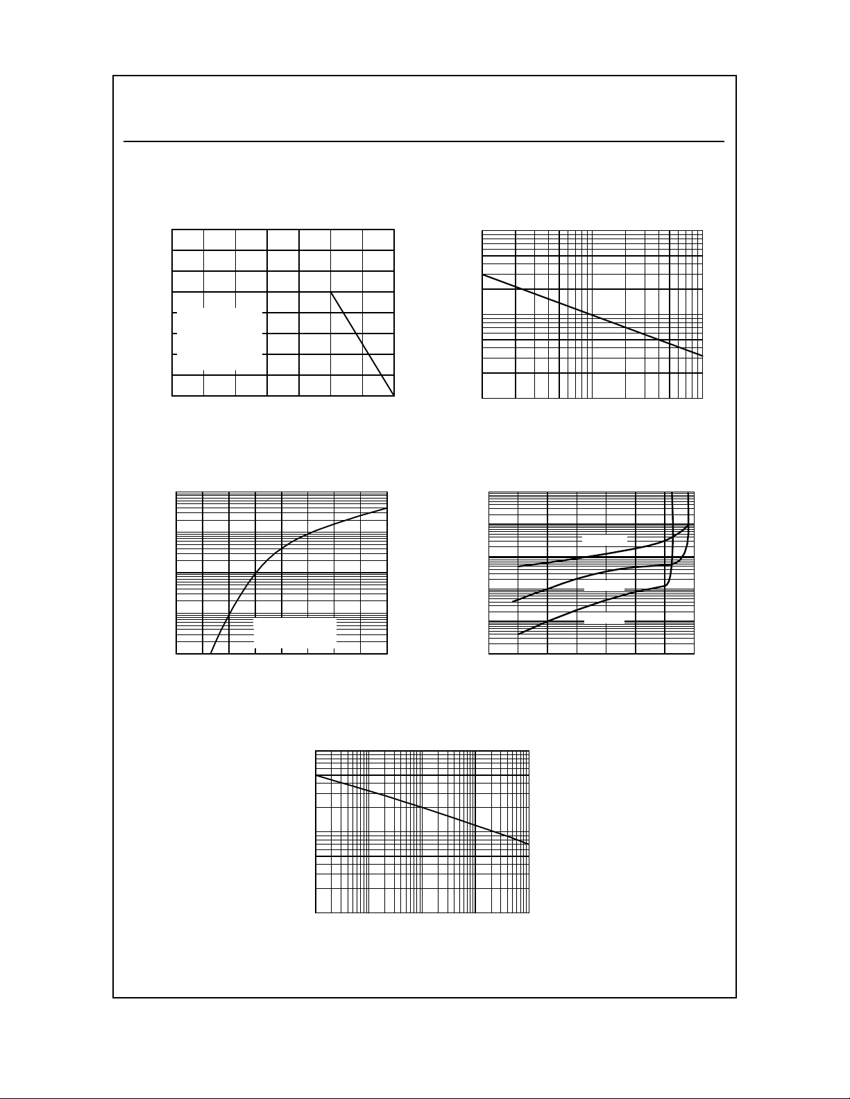
T ypical Characteristics
GF1A-GF1M
Surface Mount Glass Passivated Rectifier
(continued)
Forward Current Derating Curve
1.6
1.4
1.2
1
RESISTIVE OR
0.8
INDUCTIVE LOAD
P.C.B. MOUN T ED
0.6
ON 0.2 x 0.2 "
(5.0 x 5.0 m m)
0.4
COPPE R PAD AREAS
FORWARD CURRE NT (A)
0.2
0
0 25 50 75 100 125 150 175
LEAD TEMPERATURE ( C)
º
Forward Charact eristics
100
10
1
0.1
FORWARD CURRE NT (A)
0.01
0.4 0.6 0.8 1 1.2 1.4 1.6 1.8 2
T = 25 C
º
A
Pulse Width = 300µS
2% Duty Cycle
FORWARD VOL TAGE (V)
Non-Repetitive Surge Current
100
50
20
10
5
2
1
PEAK FORWARD SURGE CURRENT (A)
1 2 5 10 20 50 100
NUMBER OF CYCLES AT 60Hz
Reverse Characteris tics
100
10
µ
1
0.1
0.01
REVERSE CURRENT ( A)
0.001
0 20406080100120140
PERCENT OF RATED PEA K REVERSE VOL TAGE (%)
T = 125 C
º
A
º
T = 75 C
A
T = 25 C
º
A
Typical Junction Capacitance
100
50
20
10
5
2
JUNCTIO N CAPACIT A NCE (pF)
1
0.01 0.1 1 10 100
REVERSE VOLTAGE (V)
GF1A-GF1M, Rev. E
Page 3
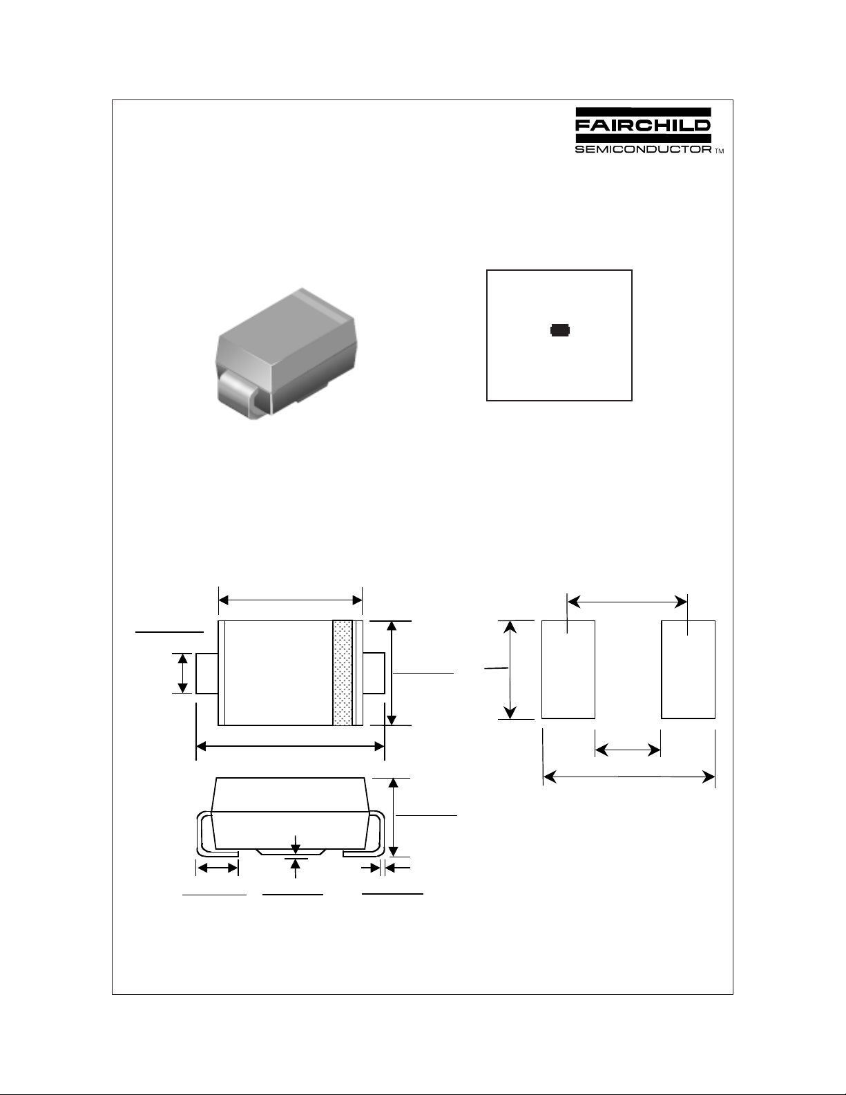
SMA/DO-214AC Package Dimensions
SMA/DO-214AC (FS PKG Code P5)
1:1
Scale 1:1 on letter size paper
Dimensions shown below are in:
inches [millimeters]
Part Weight per unit (gram): 0.064
0.062 (1.575)
0.055 (1.397)
0.060 (1.524)
0.030 (0.762)
0.181 (4.597)
0.157 (3.988)
2
0.208 (5.283)
0.188 (4.775)
0.008 (0.203)
0.002 (0.051)
0.114 (2.896)
1
0.098 (2.489)
0.096 (2.438)
0.078 (1.981)
0.012 (0.305)
0.006 (0.152)
1.67
1.47
Minimum Recommended
3.93
3.73
+
2.38
2.18
5.49
5.29
Land Pattern
August 1999, Rev. A
Page 4
TRADEMARKS
The following are registered and unregistered trademarks Fairchild Semiconductor owns or is authorized to use and is
not intended to be an exhaustive list of all such trademarks.
ACEx™
Bottomless™
CoolFET™
CROSSVOLT™
2
CMOS
E
TM
FACT™
FACT Quiet Series™
FAST
FASTr™
GTO™
HiSeC™
ISOPLANAR™
MICROWIRE™
POP™
PowerTrench
QFET™
QS™
Quiet Series™
SuperSOT™-3
SuperSOT™-6
SuperSOT™-8
SyncFET™
TinyLogic™
UHC™
VCX™
DISCLAIMER
FAIRCHILD SEMICONDUCTOR RESERVES THE RIGHT TO MAKE CHANGES WITHOUT FURTHER
NOTICE TO ANY PRODUCTS HEREIN TO IMPROVE RELIABILITY, FUNCTION OR DESIGN. FAIRCHILD
DOES NOT ASSUME ANY LIABILITY ARISING OUT OF THE APPLICATION OR USE OF ANY PRODUCT
OR CIRCUIT DESCRIBED HEREIN; NEITHER DOES IT CONVEY ANY LICENSE UNDER ITS PATENT
RIGHTS, NOR THE RIGHTS OF OTHERS.
LIFE SUPPORT POLICY
FAIRCHILD’S PRODUCTS ARE NOT AUTHORIZED FOR USE AS CRITICAL COMPONENTS IN LIFE SUPPORT
DEVICES OR SYSTEMS WITHOUT THE EXPRESS WRITTEN APPROVAL OF FAIRCHILD SEMICONDUCTOR CORPORATION.
As used herein:
1. Life support devices or systems are devices or
systems which, (a) are intended for surgical implant into
the body, or (b) support or sustain life, or (c) whose
failure to perform when properly used in accordance
with instructions for use provided in the labeling, can be
reasonably expected to result in significant injury to the
user.
2. A critical component is any component of a life
support device or system whose failure to perform can
be reasonably expected to cause the failure of the life
support device or system, or to affect its safety or
effectiveness.
PRODUCT STA TUS DEFINITIONS
Definition of Terms
Datasheet Identification Product Status Definition
Advance Information
Preliminary
No Identification Needed
Obsolete
Formative or
In Design
First Production
Full Production
Not In Production
This datasheet contains the design specifications for
product development. Specifications may change in
any manner without notice.
This datasheet contains preliminary data, and
supplementary data will be published at a later date.
Fairchild Semiconductor reserves the right to make
changes at any time without notice in order to improve
design.
This datasheet contains final specifications. Fairchild
Semiconductor reserves the right to make changes at
any time without notice in order to improve design.
This datasheet contains specifications on a product
that has been discontinued by Fairchild semiconductor.
The datasheet is printed for reference information only.
Rev. E
 Loading...