

Datasheet GAL20XV10B-20LP, GAL20XV10B-20LJ, GAL20XV10B-15LP, GAL20XV10B-15LJ, GAL20XV10B-10LP Datasheet (Lattice Semiconductor Corporation)
...Page 1
GAL20XV10
High-Speed E2CMOS PLD
Generic Array Logic™
Features
• HIGH PERFORMANCE E2CMOS ® TECHNOLOGY
— 10 ns Maximum Propagation Delay
— Fmax = 100 MHz
— 7 ns Maximum from Clock Input to Data Output
— TTL Compatible 16 mA Outputs
— UltraMOS® Advanced CMOS Technology
• 50% to 75% REDUCTION IN POWER FROM BIPOLAR
— 90mA Maximum Icc
— 75mA Typical Icc
• ACTIVE PULL-UPS ON ALL PINS
• E2 CELL TECHNOLOGY
— Reconfigurable Logic
— Reprogrammable Cells
— 100% Tested/100% Yields
— High Speed Electrical Erasure (<100 ms)
— 20 Year Data Retention
• TEN OUTPUT LOGIC MACROCELLS
— XOR Gate Capability on all Outputs
— Full Function and Parametric Compatibility with
PAL12L10, 20L10, 20X10, 20X8, 20X4
— Registered or Combinatorial with Polarity
• PRELOAD AND POWER-ON RESET OF ALL REGISTERS
• APPLICATIONS INCLUDE:
— High Speed Counters
— Graphics Processing
— Comparators
• ELECTRONIC SIGNA TURE FOR IDENTIFICATION
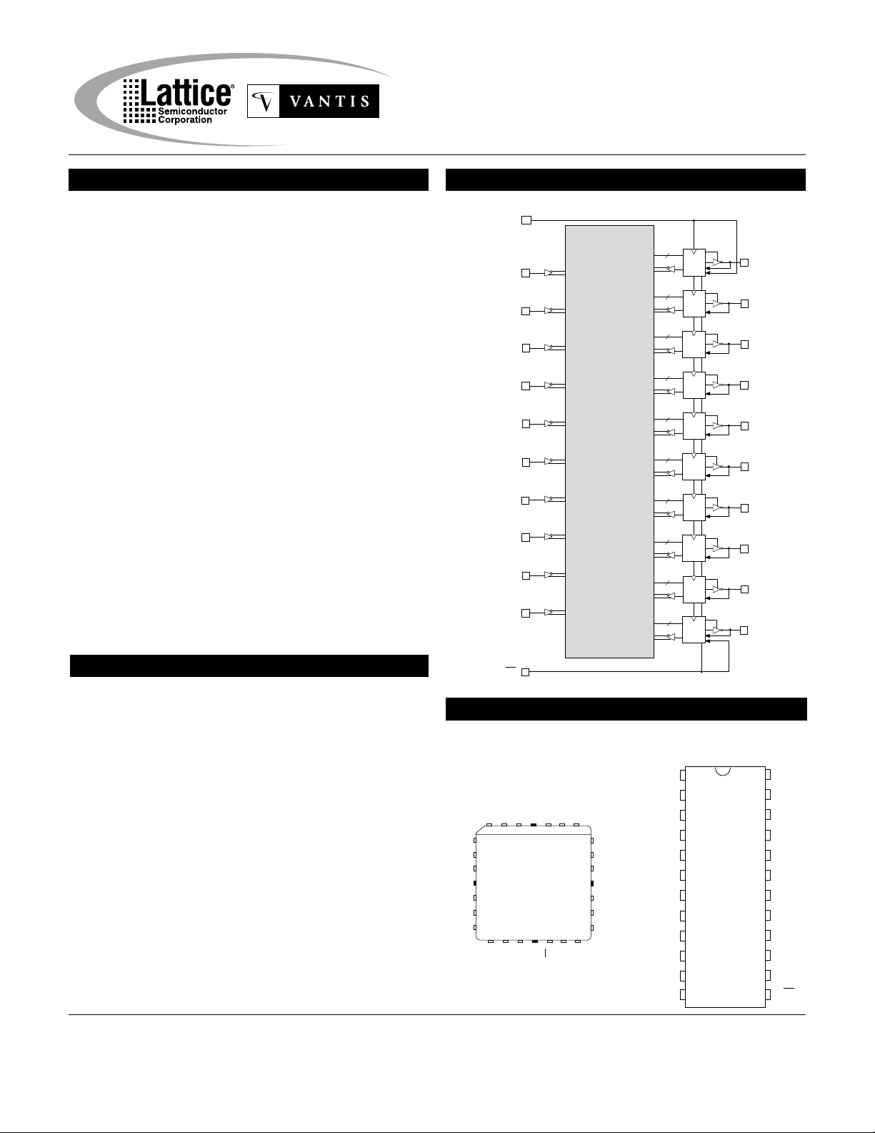
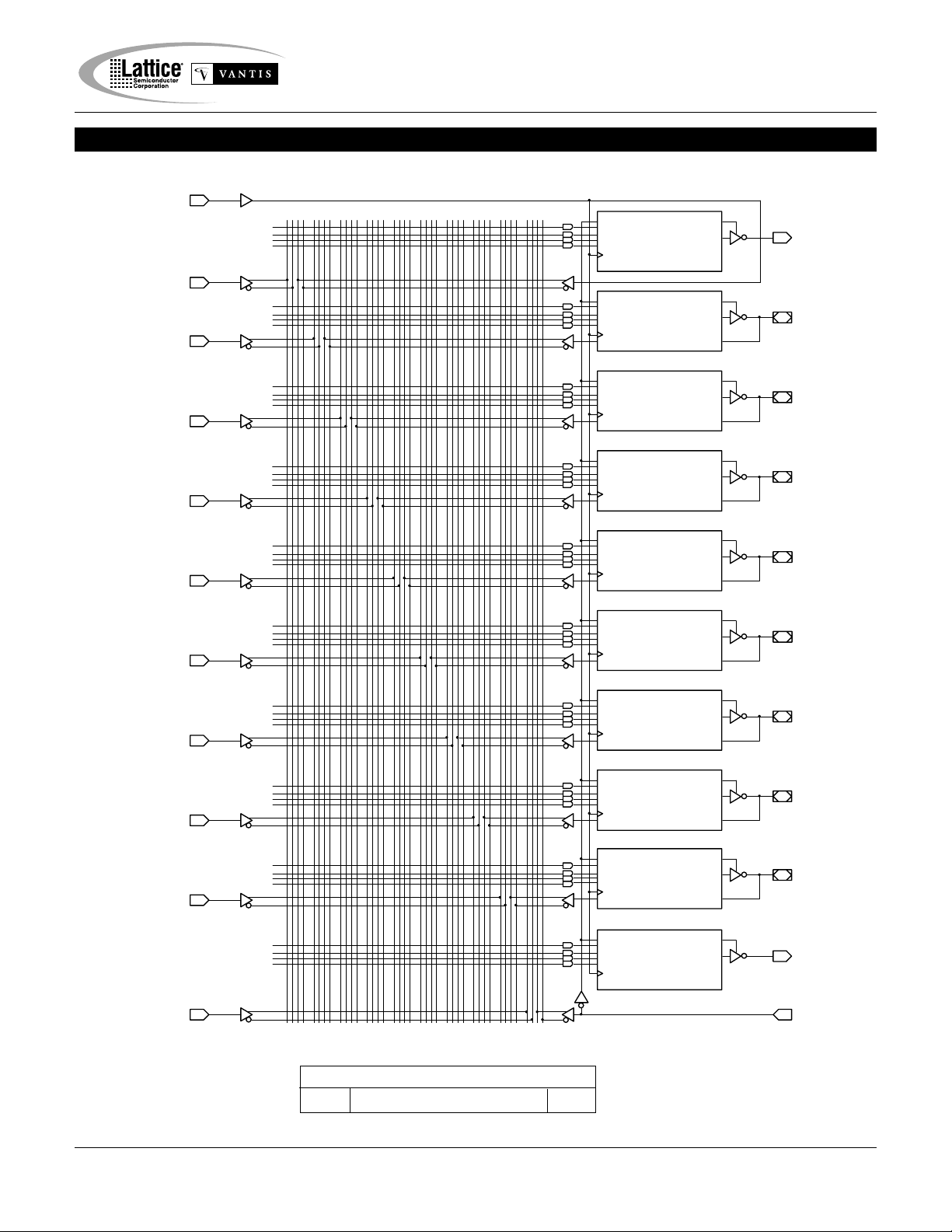
Functional Block Diagram
I/CLK
I
I
I
I
I
I
(40 X 40)
I
AND-ARRAY
PROGRAMMABLE
I
I
I
4
OLMC
4
OLMC
4
OLMC
4
OLMC
4
OLMC
4
OLMC
4
OLMC
4
OLMC
4
OLMC
4
OLMC
I/O/Q
I/O/Q
I/O/Q
I/O/Q
I/O/Q
I/O/Q
I/O/Q
I/O/Q
I/O/Q
I/O/Q
Description
The GAL20XV10 combines a high performance CMOS process
with electrically erasable (E2) floating gate technology to provide
Pin Configuration
I/OE
the highest speed Exclusive-OR PLD available in the market. At
I
I
I
I
I
I
I
I
I
I
DIP
1
GAL
20XV10
6
12
Vcc
24
I/O/Q
I/O/Q
I/O/Q
I/O/Q
I/O/Q
18
I/O/Q
I/O/Q
I/O/Q
I/O/Q
I/O/Q
13
I/OE
90mA maximum Icc (75mA typical Icc), the GAL20XV10 provides
a substantial savings in power when compared to bipolar counterparts. E2CMOS technology offers high speed (<100ms) erase
PLCC
I/CLK
times providing the ability to reprogram, reconfigure or test the devices quickly and efficiently .
The generic architecture provides maximum design flexibility by
allowing the Output Logic Macrocell (OLMC) to be configured by
the user. An important subset of the many architecture configurations possible with the GAL20XV10 are the PAL® architectures
listed in the macrocell description section of this document. The
GAL20XV10 is capable of emulating these PAL architectures with
full function and parametric compatibility.
Unique test circuitry and reprogrammable cells allow complete AC,
DC, and functional testing during manufacturing. As a result, Lattice
I
4
5
I
I
I
7
GAL20XV10
NC
I
9
I
I
11
12
I
I
2
T op View
14 16 18
I
I/CLK
GND
I/O/Q
I/O/Q
NC
Vcc
26
28
25
I/O/Q
I/O/Q
23
I/O/Q
NC
I/O/Q
21
I/O/Q
19
I/O/Q
NC
I/OE
I/O/Q
I/O/Q
Semiconductor delivers 100% field programmability and functionality of all GAL products. In addition, 100 erase/write cycles and
data retention in excess of 20 years are specified.
Copyright © 1997 Lattice Semiconductor Corp. All brand or product names are trademarks or registered trademarks of their respective holders. The specifications and information herein are subject
to change without notice.
LATTICE SEMICONDUCTOR CORP., 5555 Northeast Moore Ct., Hillsboro, Oregon 97124, U.S.A. July 1997
Tel. (503) 681-0118; 1-888-ISP-PLDS; FAX (503) 681-3037; http://www.latticesemi.com
20xv10_02
1
GND
Page 2
GAL20XV10 Ordering Information
Commercial Grade Specifications
)sn(dpT)sn(usT)sn(ocT)Am(ccI#gniredrOegakcaP
016709PL01-B01VX02LAGPIDcitsalPniP-42
JL01-B01VX02LAGCCLPdaeL-82
518809PL51-B01VX02LAGPIDcitsalPniP-42
JL51-B01VX02LAGCCLPdaeL-82
02010109PL02-B01VX02LAGPIDcitsalPniP-42
JL02-B01VX02LAGCCLPdaeL-82
Part Number Description
Specifications GAL20XV10
GAL20XV10B
Device Name
Speed (ns)
PowerL = Low Power
XXXXXXXX XX X X X
_
Grade
Package
Blank = Commercial
P = Plastic DIP
J = PLCC
2
Page 3
Output Logic Macrocell (OLMC)
Specifications GAL20XV10
The following discussion pertains to configuring the Output Logic
Macrocell. It should be noted that actual implementation is
accomplished by development software/hardware and is completely transparent to the user.
The GAL20XV10 has two global architecture configurations that
allow it to emulate P AL architectures. The Input mode emulates
combinatorial PAL devices, with the I/CLK and I/OE pins used as
inputs. The Feedback mode emulates registered P AL devices with
the I/CLK pin used as the register clock and the I/OE pin as an
output enable for all registers. The following is a list of P AL architectures that the GAL20XV10 can emulate. It also shows the
global architecture mode used to emulate the P AL architecture.
P AL Architectures Emulated by
GAL20XV10
PAL12L10
PAL20L10
PAL20X10
PAL20X8
PAL20X4
INPUT MODE
The Input mode architecture is defined when the global
architecture bit SYN = 1. In this mode, the I/CLK pin becomes an
input to the AND array and also provides the clock source for
all registers. The I/OE pin becomes an input into the AND array
and provides the output enable control for any macrocell configured as an Exclusive-OR function. Feedback into the AND array
is provided from macrocells 2 through 9 only. In this mode,
macrocells 1 and 10 have no feedback into the AND array.
FEEDBACK MODE
The Feedback mode architecture is defined when the global
architecture bit SYN = 0. In this mode the I/CLK pin becomes a
dedicated clock source for all registers. The I/OE pin is a dedicated output enable control for any macrocell configured as an
Exclusive-OR function. The I/CLK and I/OE pins are not available to the AND array in this mode. Feedback into the AND array
is provided on all macrocells 1 through 10.
FEATURES
Each Output Logic Macrocell has four possible logic function
configurations controlled by architecture control bits AC0 and AC1.
Four product terms are fed into each macrocell.
GAL20XV10 Global
OLMC Mode
Input Mode
Input Mode
Feedback Mode
Feedback Mode
Feedback Mode
Exclusive-OR macrocells. In Feedback mode, the state of the
register is available to the AND array via an internal feedback
path on all macrocells. In Input mode, the state of the register
is available to the AND array via an internal feedback path on
macrocells 2 through 9 only , macrocells 1 and 10 have no feedback
into the AND array.
REGISTERED CONFIGURATION
The Macrocell is set to Registered configuration when AC0 = 1 and
AC1 = 0. Three of the four product terms are used as sum-ofproduct terms for the D input of the register. The inverting output
buffer is enabled by the fourth product term. The output is enabled while this product term is true. The XOR bit controls the polarity of the output. The register is clocked by the low-to-high transition of the I/CLK. In Feedback mode, the state of the register
is available to the AND array via an internal feedback path on
all macrocells. In Input mode, the state of the register is available
to the AND array via an internal feedback path on macrocells
2 through 9 only, macrocells 1 and 10 have no feedback into the
AND array .
XOR COMBINA TORIAL CONFIGURATION
The Macrocell is set to the Exclusive-OR Combinatorial configuration when AC0 = 0 and AC1 = 1. The four product terms are segmented into two OR-sums of two product terms each, which are
then combined by an Exclusive-OR gate and fed to an output
buffer. The inverting output buffer is enabled by the I/OE pin,
which is an active low output enable that is common to all XOR
macrocells. In Feedback mode, the state of the I/O pin is available to the AND array via an internal feedback path on all
macrocells. In Input mode, the state of the I/O pin is available to
the AND array via an input buf fer path on macrocells 2 through
9 only , macrocells 1 and 10 have no input into the AND array.
COMBINAT ORIAL CONFIGURATION
The Macrocell is set to Combinatorial mode when AC0 = 1 and
AC1 = 1. Three of the four product terms are used as sum-ofproduct terms for the combinatorial output. The XOR bit controls
the polarity of the output. The inverting output buffer is enabled
by the fourth product term. The output is enabled while this product
term is true. In Feedback mode, the state of the I/O pin is available to the AND array via an internal feedback path on all
macrocells. In Input mode, the state of the I/O pin is available
to the AND array via an input buffer path on macrocells 2 through
9 only , macrocells 1 and 10 have no input into the AND array.
XOR REGISTERED CONFIGURA TION
The Macrocell is set to the Exclusive-OR Registered configuration
when AC0 = 0 and AC1 = 0. The four product terms are segmented into two OR-sums of two product terms each, which are
then combined by an Exclusive-OR gate and fed into a D-type
register. The register is clocked by the low-to-high transition of the
I/CLK pin. The inverting output buffer is enabled by the
I/OE pin, which is an active low output enable common to all
3
Page 4
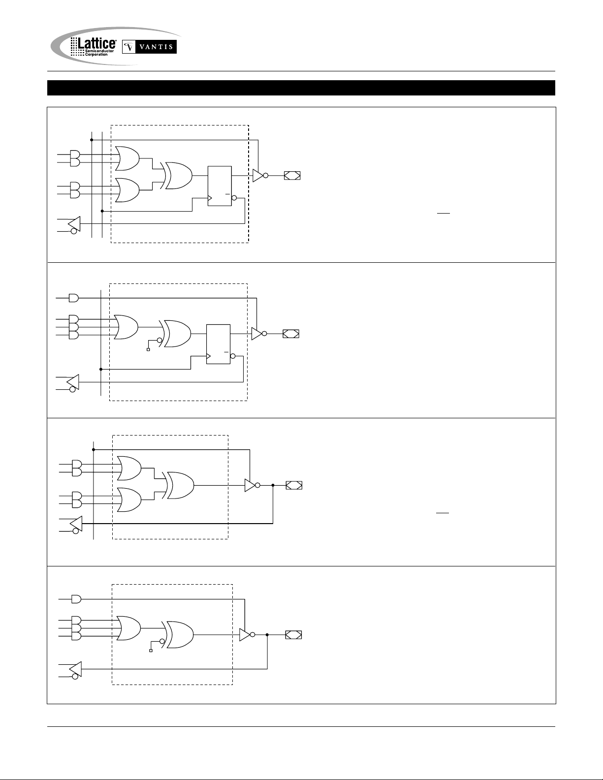
Input Mode
OE
CLK
CLK
XOR
Specifications GAL20XV10
XOR Registered Configuration
- SYN = 1.
- AC0 = 0.
D
Q
Q
Registered Configuration
D
Q
Q
- AC1 = 0.
- OLMC 1 and OLMC10 do not have the
feedback path.
- Pin 1(2) can be CLK and/or Input.
- Pin 13(16) can be OE and/or Input.
- SYN = 1.
- AC0 = 1.
- AC1 = 0.
- XOR = 1 defines Active Low Output.
- XOR = 0 defines Active High Output.
- OLMC 1 and OLMC10 do not have the
feedback path.
- Pin 1(2) can be CLK and/or Input.
- OE controlled by product term.
OE
XOR
XOR Combinatorial Configuration
- SYN = 1.
- AC0 = 0.
- AC1 = 1.
- OLMC 1 and OLMC10 do not have the
feedback path.
- Pin 13(16) can be OE and/or Input.
Combinatorial Configuration
- SYN = 1.
- AC0 = 1.
- AC1 = 1.
- XOR = 1 defines Active Low Output.
- XOR = 0 defines Active High Output.
- OLMC 1 and OLMC10 do not have the
feedback path.
- OE controlled by product term.
4
Page 5
Input Mode Logic Diagram
1(2)
0
120
2(3)
160
280
3(4)
Specifications GAL20XV10
DIP (PLCC) Package Pinouts
2812 16 20 24 32 36048
OLMC
XOR - 1600
AC0 - 1610
AC1 - 1620
OLMC
XOR - 1601
AC0 - 1611
AC1 - 1621
23(27)
22(26)
4(5)
5(6)
6(7)
7(9)
8(10)
9(11)
320
440
480
600
640
760
800
920
960
1080
1120
1240
OLMC
XOR - 1602
AC0 - 1612
AC1 - 1622
OLMC
XOR - 1603
AC0 - 1613
AC1 - 1623
OLMC
XOR - 1604
AC0 - 1614
AC1 - 1624
OLMC
XOR - 1605
AC0 - 1615
AC1 - 1625
OLMC
XOR - 1606
AC0 - 1616
AC1 - 1626
OLMC
XOR - 1607
AC0 - 1617
AC1 - 1627
21(25)
20(24)
19(23)
18(21)
17(20)
16(19)
10(12)
11(13)
1280
1400
1440
1560
40-USER ELECTRONIC SIGNA TURE FUSES
1631, 1632, .... .... 1669, 1670
Byte4 Byte3 .... .... Byte1 Byte0
5
OLMC
XOR - 1608
AC0 - 1618
AC1 - 1628
OLMC
XOR - 1609
AC0 - 1619
AC1 - 1629
15(18)
14(17)
13(16)
SYN - 1630
Page 6

Feedback Mode
OE
CLK
CLK
XOR
Specifications GAL20XV10
XOR Registered Configuration
- SYN = 0.
D
Q
Q
Registered Configuration
D
Q
Q
- AC0 = 0.
- AC1 = 0.
- Dedicated CLK input on Pin 1(2).
- Dedicated OE input on Pin 13(16).
- SYN = 0.
- AC0 = 1.
- AC1 = 0.
- XOR = 1 defines Active Low Output.
- XOR = 0 defines Active High Output.
- Dedicated CLK input on Pin 1(2).
- OE controlled by product term.
- Pin 13(16) is not connected to this configura tion.
OE
XOR
XOR Combinatorial Configuration
- SYN = 0.
- AC0 = 0.
- AC1 = 1.
- Dedicated OE input on Pin 13(16).
- Pin 1(2) is not connected to this configura tion.
Combinatorial Configuration
- SYN = 0.
- AC0 = 1.
- AC1 = 1.
- XOR = 1 defines Active Low Output.
- XOR = 0 defines Active High Output.
- OE controlled by product term.
- Both pin1(2) and pin 13(16) are not con nected to this configuration.
6
Page 7

Feedback Mode Logic Diagram
1(2)
0
120
2(3)
Specifications GAL20XV10
DIP (PLCC) Package Pinouts
2812 16 20 24 32 36048
OLMC
XOR - 1600
AC0 - 1610
AC1 - 1620
23(27)
3(4)
4(5)
5(6)
6(7)
7(9)
8(10)
160
280
320
440
480
600
640
760
800
920
960
1080
OLMC
XOR - 1601
AC0 - 1611
AC1 - 1621
OLMC
XOR - 1602
AC0 - 1612
AC1 - 1622
OLMC
XOR - 1603
AC0 - 1613
AC1 - 1623
OLMC
XOR - 1604
AC0 - 1614
AC1 - 1624
OLMC
XOR - 1605
AC0 - 1615
AC1 - 1625
OLMC
XOR - 1606
AC0 - 1616
AC1 - 1626
22(26)
21(25)
20(24)
19(23)
18(21)
17(20)
9(11)
10(12)
11(13)
1120
1240
1280
1400
1440
1560
40-USER ELECTRONIC SIGNA TURE FUSES
1631, 1632, .... .... 1669, 1670
Byte4 Byte3 .... .... Byte1 Byte0
7
OLMC
XOR - 1607
AC0 - 1617
AC1 - 1627
OLMC
XOR - 1608
AC0 - 1618
AC1 - 1628
OLMC
XOR - 1609
AC0 - 1619
AC1 - 1629
16(19)
15(18)
14(17)
13(16)
SYN - 1630
Page 8

Specifications GAL20XV10
Absolute Maximum Ratings
Supply voltage Vcc.......................................–0.5 to+7V
Input voltage applied ..........................–2.5 to
Off-state output voltage applied .........–2.5 to
Storage T emperature ............................... –65 to 150°C
Ambient Temperature with
Power Applied .......................................... –55 to 125°C
1.Stresses above those listed under the “Absolute Maximum
Ratings” may cause permanent damage to the device. These
are stress only ratings and functional operation of the device at
these or at any other conditions above those indicated in the
operational sections of this specification is not implied (while programming, follow the programming specifications).
(1)
VCC +1.0V
VCC +1.0V
Recommended Operating Conditions
Commercial Devices:
Ambient T emperature (
Supply voltage (
with Respect to Ground ..................... +4.75 to +5.25V
TA) .............................0 to +75°C
VCC)
DC Electrical Characteristics
Over Recommended Operating Conditions (Unless Otherwise Specified)
SYMBOL PARAMETER CONDITION MIN. TYP.3MAX. UNITS
VIL Input Low Voltage VSS – 0.5 — 0.8 V
VIH Input High Voltage 2.0 — VCC+1 V
1
IIL
Input or I/O Low Leakage Current 0V ≤ VIN ≤ VIL (MAX.) ——–100 µA
IIH Input or I/O High Leakage Current 3.5V ≤ VIN ≤ VCC ——10 µA
VOL Output Low Voltage IOL = MAX. Vin = VIL or VIH ——0.5 V
VOH Output High Voltage IOH = MAX. Vin = VIL or VIH 2.4 ——V
IOL Low Level Output Current ——16 mA
IOH High Level Output Current ——–3.2 mA
2
IOS
Output Short Circuit Current VCC = 5V VOUT = 0.5V TA= 25°C –50 —–150 mA
COMMERCIAL
ICC Operating Power VIL = 0.5V VIH = 3.0V L -10/-15/-20 — 75 90 mA
Supply Current f
1) The leakage current is due to the internal pull-up on all input and I/O pins. See Input Buffer section for more information.
2) One output at a time for a maximum duration of one second. Vout = 0.5V was selected to avoid test problems by tester
ground degradation. Characterized but not 100% tested.
3) Typical values are at V CC = 5V and TA = 25 °C
toggle = 15MHz Outputs Open
8
Page 9

AC Switching Characteristics
Specifications GAL20XV10
Over Recommended Operating Conditions
COM
PARAMETER UNITS
TEST
COND.
DESCRIPTION
1
-10
MIN. MAX.
COM
-15
MIN. MAX.
COM
-20
MIN. MAX.
tpd A Input or I/O to Combinatorial Output 3 10 3 15 3 20 ns
tco A Clock to Output Delay 2 7 2 8 2 10 ns
tcf
2
— Clock to Feedback Delay — 4 — 4 — 4ns
tsu — Setup Time, Input or Feedback before Clock↑ 6 — 8 — 10 — ns
th — Hold Time, Input or Feedback after Clock↑ 0 — 0 — 0 — ns
fmax
A Maximum Clock Frequency with 76.9 — 62.5 — 50 — MHz
3
A Maximum Clock Frequency with 100 — 83.3 — 71.4 — MHz
A Maximum Clock Frequency with 100 — 83.3 — 71.4 — MHz
External Feedback, 1/(tsu + tco)
Internal Feedback, 1/(tsu + tcf)
No Feedback
twh — Clock Pulse Duration, High 4 — 6 — 7 — ns
twl — Clock Pulse Duration, Low 4 — 6 — 7 — ns
ten
tdis
B Input or I/O to Output Enabled 3 10 3 15 3 20 ns
B OE to Output Enabled 2 9 2 10 2 15 ns
C Input or I/O to Output Disabled 3 9 3 15 3 20 ns
C OE to Output Disabled 2 9 2 10 2 15 ns
1) Refer to Switching Test Conditions section.
2) Calculated from fmax with internal feedback. Refer to fmax Description section.
3) Refer to fmax Description section.
Capacitance (TA = 25°C, f = 1.0 MHz)
SYMBOL PARAMETER MAXIMUM* UNITS TEST CONDITIONS
I Input Capacitance 8 pF VCC = 5.0V, VI = 2.0V
C
CI/O I/O Capacitance 8 pF VCC = 5.0V, VI/O = 2.0V
*Characterized but not 100% tested
9
Page 10

Switching Waveforms
Specifications GAL20XV10
INPUT or
I/O FEEDBACK
COMBINATORIAL
OUTPUT
VALID INPUT
t
pd
Combinatorial Output
INPUT or
I/O FEEDBACK
t
dis
OUTPUT
Input or I/O Feedback to Enable/Disable
t
wl
CLK
t
wh
1/ fmax
(w/o fdbk)
Clock Width
INPUT or
I/O FEEDBACK
CLK
REGISTERED
OUTPUT
VALID INPUT
t
su
t
t
1/ fmax
(external fdbk)
h
co
Registered Output
OE
dis
t
en
OUTPUT
OEOE
OE to Output Enable/Disable
OEOE
CLK
REGISTERED
FEEDBACK
t
1/fmax (internal fdbk)
cf
t
en
t
su
t
fmax with Feedback
Input/Output Equivalent Schematics
PIN
(Vref Typical = 3.2V)
ESD
Protection
Circuit
PIN
Active Pull-up
Circuit
Vcc
Vref
ESD
Protection
Circuit
Typical Input T ypical Output
Vcc
Vcc
10
Data
Output
Feedback
Tri-State
Control
Active Pull-up
Circuit
Vcc
Feedback
(To Input Buffer)
Vref
PIN
(Vref Typical = 3.2V)
PIN
Page 11

fmax Descriptions
Specifications GAL20XV10
CLK
LOGIC
ARRAY
t
su
REGISTER
t
co
fmax with External Feedback 1/(tsu+tco)
Note: fmax with external feedback is calculated from measured
tsu and tco.
CLK
LOGIC
ARRAY
t
su + th
REGISTER
fmax with No Feedback
Note: fmax with no feedback may be less than 1/(twh + twl). This
is to allow for a clock duty cycle of other than 50%.
CLK
LOGIC
ARRAY
REGISTER
t
cf
t
pd
fmax with Internal Feedback 1/(tsu+tcf)
Note: tcf is a calculated value, derived by subtracting tsu from
the period of fmax w/internal feedback (tcf = 1/fmax - tsu). The
value of tcf is used primarily when calculating the delay from
clocking a register to a combinatorial output (through registered
feedback), as shown above. For example, the timing from clock
to a combinatorial output is equal to tcf + tpd.
Switching Test Conditions
Input Pulse Levels GND to 3.0V
Input Rise and Fall Times 3ns 10% – 90%
Input Timing Reference Levels 1.5V
Output Timing Reference Levels 1.5V
Output Load See Figure
3-state levels are measured 0.5V from steady-state active
level.
Output Load Conditions (see figure)
T est Condition R
A
Active High ∞ 390Ω 50pF
B
Active Low 300Ω 390Ω 50pF
Active High ∞ 390Ω 5pF
C
Active Low 300Ω 390Ω 5pF
1 R2 CL
300Ω 390Ω 50pF
11
+5V
R
1
FROM OUTPUT (O/Q)
UNDER TEST
R
2
INCLUDES TEST FIXTURE AND PROBE CAPACITANCE
*C
L
C *
L
TEST POINT
Page 12

Specifications GAL20XV10
Electronic Signature
An electronic signature word is provided in every GAL20XV10
device. It contains 40 bits of reprogrammable memory that contains user defined data. Some uses include user ID codes, revision numbers, pattern identification or inventory control codes. The
signature data is always available to the user independent of the
state of the security cell.
NOTE: The electronic signature bits, if programmed to any value
other then zero(0) will alter the checksum of the device.
Security Cell
A security cell is provided in every GAL20XV10 device as a deterrent to unauthorized copying of the device pattern. Once programmed, this cell prevents further read access of the device
pattern information. This cell can be only be reset by reprogramming the device. The original pattern can never be examined once
this cell is programmed. The Electronic Signature is always available regardless of the security cell state.
Device Programming
GAL devices are programmed using a Lattice Semiconductorapproved Logic Programmer, available from a number of manufacturers. Complete programming of the device takes less than a
second. Erasing of the device is transparent to the user, and is done
automatically as part of the programming cycle.
Latch-Up Protection
GAL20XV10 devices are designed with an on-board charge pump
to negatively bias the substrate. The negative bias is of sufficient
magnitude to prevent input undershoots from causing the circuitry
to latch. Additionally , outputs are designed with n-channel pullups
instead of the traditional p-channel pullups to eliminate any possibility of SCR induced latching.
Input Buffers
GAL20XV10 devices are designed with TTL level compatible input buffers. These buffers have a characteristically high impedance, and present a much lighter load to the driving logic than bipolar TTL devices.
GAL20XV10 input buffers have active pull-ups within their input
structure. This pull-up will cause any un-terminated input or
I/O to float to a TTL high (logical 1). Lattice Semiconductor
recommends that all unused inputs and tri-stated I/O pins be
connected to another active input, Vcc, or GND. Doing this will tend
to improve noise immunity and reduce Icc for the device.
T ypical Input Pull-up Characteristic
0
-20
-40
Input Current (µA)
-60
1.0 2.0 3.0 4.0 5.0
0
Input Voltage (Volts)
Power-Up Reset
Circuitry within the GAL20XV10 provides a reset signal to all registers during power-up. All internal registers will have their Q outputs
set low after a specified time (
on the registered output pins (if they are enabled) will always be
high on power-up, regardless of the programmed polarity of the
output pins. This feature can greatly simplify state machine design
by providing a known state on power-up. The timing diagram for
power-up is shown below. Because of the asynchronous nature
tpr, 1µs MAX). As a result, the state
Vcc (min.)
Vcc
CLK
INTERNAL REGISTER
Q - OUTPUT
FEEDBACK/EXTERNAL
OUTPUT REGISTER
of system power-up, some conditions must be met to provide a valid
power-up reset of the GAL20XV10. First, the V
CC rise must be
monotonic. Second, the clock input must be at static TTL level as
shown in the diagram during power up. The registers will reset
within a maximum of
tpr time. As in normal system operation, avoid
clocking the device until all input and feedback path setup times
have been met. The clock must also meet the minimum pulse width
requirements.
t
su
t
wl
t
pr
Internal Register
Reset to Logic "0"
Device Pin
Reset to Logic "1"
12
Page 13

Typical AC and DC Characteristic Diagrams
Specifications GAL20XV10
Normalized Tpd vs Vcc
1.2
1.1
1
0.9
Normalized Tpd
0.8
4.50 4.75 5.00 5.25 5.50
Supply Voltage (V)
Normalized Tpd vs Temp
1.3
1.2
1.1
1
0.9
Normalized Tpd
0.8
0.7
-55 -25 0 25 50 7 5 100 125
PT H->L
PT L->H
Temperature (deg. C)
PT H->L
PT L->H
Normalized Tco vs Vcc
1.2
1.1
1
0.9
Normalized Tco
0.8
4.50 4.75 5.00 5.25 5.50
Supply Voltage (V)
Normalized Tco vs Temp
1.3
1.2
1.1
1
0.9
Normalized Tco
0.8
0.7
-55 -25 0 25 50 75 100 125
RISE
FALL
Temperature (deg. C)
RISE
FALL
Normalized Tsu vs Vcc
1.2
1.1
1
0.9
Normalized Tsu
0.8
4.50 4.75 5.00 5.25 5.50
PT H->L
PT L->H
Supply Voltage (V)
Normalized Tsu vs Temp
1.4
1.3
1.2
1.1
1
0.9
Normalized Tsu
0.8
0.7
-55 -25 0 25 50 75 100 125
PT H->L
PT L->H
Temperature (deg. C)
Delta Tpd vs # of Outputs
Switching
0
-0.5
-1
-1.5
Delta Tpd (ns)
-2
12345678910
Number of Outputs Switching
Delta Tpd vs Output Loading
12
10
8
6
4
2
Delta Tpd (ns)
0
-2
0 50 100 150 200 250 300
RISE
FALL
Output Loading (pF)
RISE
FALL
Delta Tco vs # of Outputs
Switching
0
-0.5
-1
-1.5
Delta Tco (ns)
-2
12345678910
Number of Outputs Switching
Delta Tco vs Output Loading
12
10
8
6
4
2
Delta Tco (ns)
0
-2
0 50 100 150 200 250 300
RISE
FALL
Output Loading (pF)
RISE
FALL
13
Page 14

Typical AC and DC Characteristic Diagrams
Specifications GAL20XV10
Vol vs Iol
3
2.5
2
1.5
Vol (V)
1
0.5
0
0.00 20.00 40.00 60.00 80.00 100.00
Iol (mA)
Normalized Icc vs Vcc
1.20
1.10
1.00
0.90
Normalized Icc
0.80
4.50 4.75 5.00 5.25 5.50
Supply Voltage (V)
Voh vs Ioh
5
4
3
2
Voh (V)
1
0
0.00 10.00 20.00 30.00 40.00 50.00 60.00
Ioh(mA)
Normalized Icc vs Temp
1.2
1.1
1
0.9
Normalized Icc
0.8
-55 -25 0 25 50 75 100 125
Temperature (deg. C)
Voh vs Ioh
4.5
4.25
4
Voh (V)
3.75
3.5
0.00 1.00 2.00 3.00 4.00
Ioh(mA)
Normalized Icc vs Freq.
1.70
1.60
1.50
1.40
1.30
1.20
1.10
1.00
0.90
Normalized Icc
0.80
0.70
0 255075100
Frequency (MHz)
Delta Icc vs Vin (1 input)
10
8
6
4
Delta Icc (mA)
2
0
0.00 0.50 1.00 1.50 2.00 2.50 3.00 3.50 4.00
Vin (V)
Input Clamp (Vik)
0
20
40
60
Iik (mA)
80
100
120
-2.00 -1.50 -1.00 -0.50 0.00
Vik (V)
14
 Loading...