

Page 1
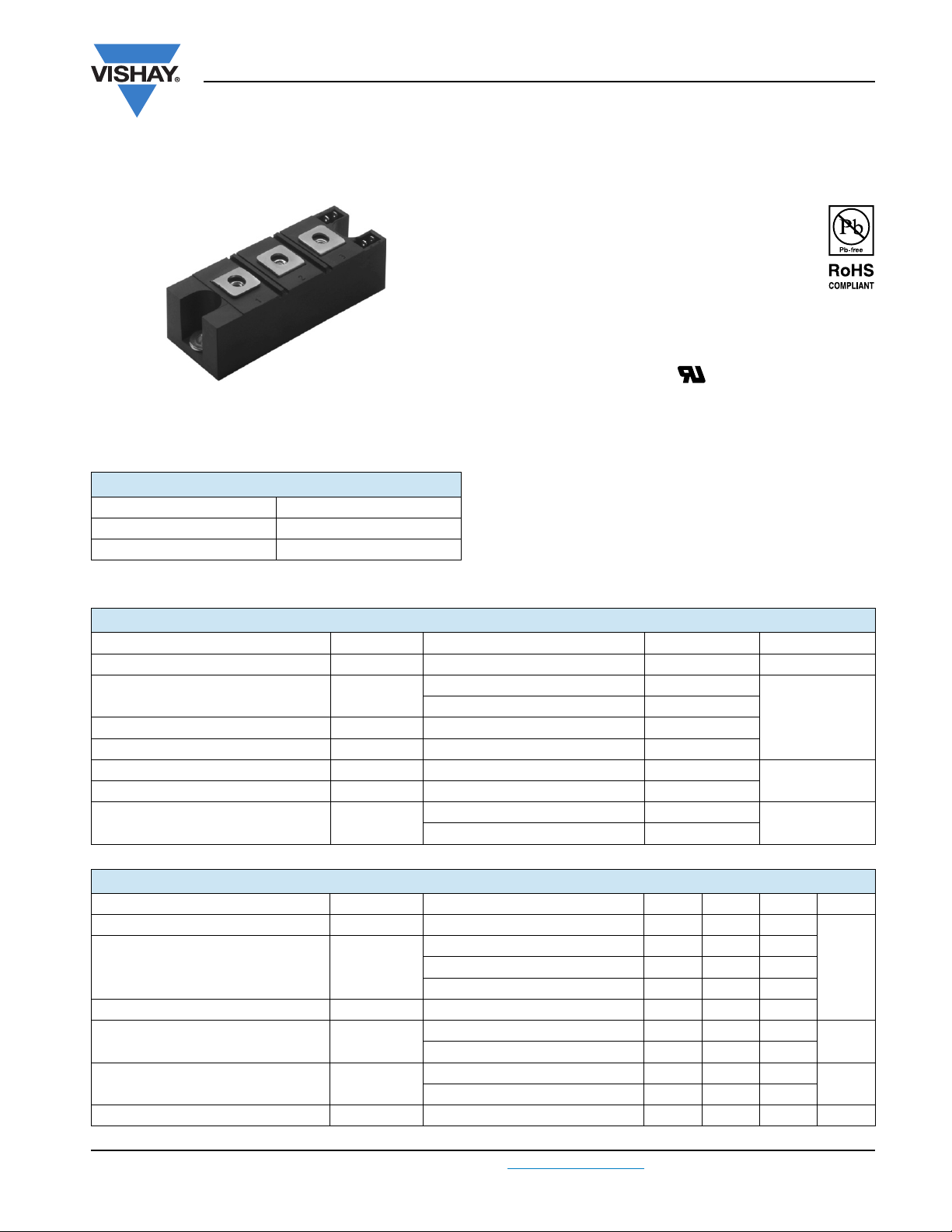
INT-A-PAK
PRODUCT SUMMARY
V
CES
DC 220 A
I
C
at 100 A, 25 °C 1.11 V
V
CE(on)
Vishay High Power Products
"Half-Bridge" IGBT INT-A-PAK
(Standard Speed IGBT), 100 A
FEATURES
• Standard speed PT IGBT technology
• Standard speed: DC to 1 kHz, optimized for
hard switching speed
2O3
®
antiparallel diodes with fast recovery
DBC
600 V
•FRED Pt
• Very low conduction losses
•Al
• UL approved file E78996
• Compliant to RoHS directive 2002/95/EC
• Designed for industrial level
BENEFITS
• Optimized for high current inverter stages (AC TIG welding
machines)
• Direct mounting to heatsink
• Very low junction to case thermal resistance
•Low EMI
GA100TS60SFPbF
ABSOLUTE MAXIMUM RATINGS
PARAMETER SYMBOL TEST CONDITIONS MAX. UNITS
Collector to emitter voltage V
Continuous collector current I
Pulsed collector current I
Peak switching current I
Gate to emitter voltage V
RMS isolation voltage V
Maximum power dissipation P
CES
C
CM
LM
GE
ISOL
D
TC = 25 °C 220
= 130 °C 100
T
C
Any terminal to case, t = 1 min 2500
TC = 25 °C 780
T
= 100 °C 312
C
600 V
440
440
± 20
A
V
W
ELECTRICAL SPECIFICATIONS (TJ = 25 °C unless otherwise specified)
PARAMETER SYMBOL TEST CONDITIONS MIN. TYP. MAX. UNITS
Collector to emitter breakdown voltage V
Gate threshold voltage V
Collector to emitter leakage current I
Diode forward voltage drop V
Gate to emitter leakage current I
BR(CES)
CE(on)
GE(th)
CES
FM
GES
VGE = 0 V, IC = 1 mA 600 - -
VGE = 15 V, IC = 100 A - 1.11 1.28
= 200 A - 1.39 -
I
C
= 15 V, IC = 100 A, TJ = 125 °C - 1.08 1.22
V
GE
IC = 0.25 mA 3 - 6
VGE = 0 V, VCE = 600 V - - 1
V
= 0 V, VCE = 600 V, TJ = 125 °C - - 10
GE
IC = 100 A, VGE = 0 V - 1.44 1.96
I
= 100 A, VGE = 0 V, TJ = 125 °C - 1.25 1.54
C
VGE = ± 20 V - - ± 250 nA
www.vishay.com
mA
VCollector to emitter voltage V
V
Page 2
GA100TS60SFPbF
Vishay High Power Products
"Half-Bridge" IGBT INT-A-PAK
(Standard Speed IGBT), 100 A
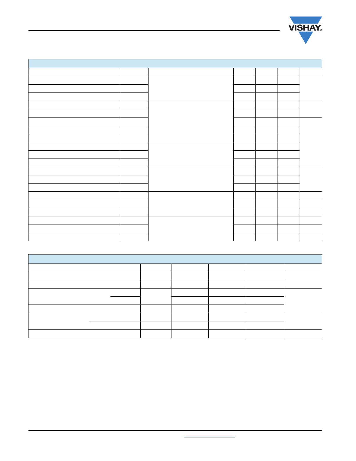
SWITCHING CHARACTERISTICS (TJ = 25 °C unless otherwise specified)
PARAMETER SYMBOL TEST CONDITIONS MIN. TYP. MAX. UNITS
Total gate charge Q
Gate to collector charge Q
Rise time t
Fall time t
Turn-on switching energy E
Turn-off switching energy E
Total switching energy E
Turn-on switching energy E
Turn-off switching energy E
Total switching energy E
Input capacitance C
Reverse transfer capacitance C
Diode reverse recovery time t
Diode peak reverse current I
Diode recovery charge Q
Diode reverse recovery time t
Diode peak reverse current I
Diode recovery charge Q
ge
gc
on
off
on
off
ies
oes
res
rr
rr
rr
rr
g
r
f
ts
IC = 100 A
= 400 V
V
CC
= 15 V
V
GE
IC = 100 A
V
= 480 V
CC
= 15 V
V
GE
= 15 Ω
R
g
T
= 25 °C
J
IC = 100 A, VCC = 480 V
= 15 V, Rg = 15 Ω
V
GE
= 125 °C
T
ts
J
VGE = 0 V
= 30 V
V
CC
f = 1.0 MHz
IF = 50 A
dI
/dt = 200 A/μs
F
= 200 V
V
rr
RR
IF = 50 A
dI
/dt = 200 A/μs
F
V
= 200 V, TJ = 125 °C
rr
RR
- 640 700
- 108 120
- 230 300
-0.45-
-1.0-
-46
-2329
-2735
-612
-3540
-4152
- 16 250 -
- 1040 -
- 190 -
- 91 155 ns
-10.615 A
- 500 900 nC
- 180 344 ns
- 17 20.5 A
- 1633 2315 nC
nCGate to emitter charge Q
μs
mJ
pFOutput capacitance C
THERMAL AND MECHANICAL SPECIFICATIONS
PARAMETER SYMBOL MIN. TYP. MAX. UNITS
Operating junction temperature range T
Storage temperature range T
Junction to case
per switch
Case to sink per module R
Mounting torque
case to heatsink - - 4
case to terminal 1, 2, 3 - - 3
J
Stg
R
thJC
thCS
Weight - 185 - g
- 40 - 150
- 40 - 125
--0.16
-0.1 -
Document Number: 94544
°C
°C/Wper diode - - 0.48
Nm
Page 3
GA100TS60SFPbF
"Half-Bridge" IGBT INT-A-PAK
(Standard Speed IGBT), 100 A
1000
Vge = 15V
100
Tj = 25˚C
, Collector-to-Emitter Current (A)
C
I
10
0.6 0.8 1 1.2 1.4 1.6 1.8
VCE, Collector-to-Emitter Voltage (V)
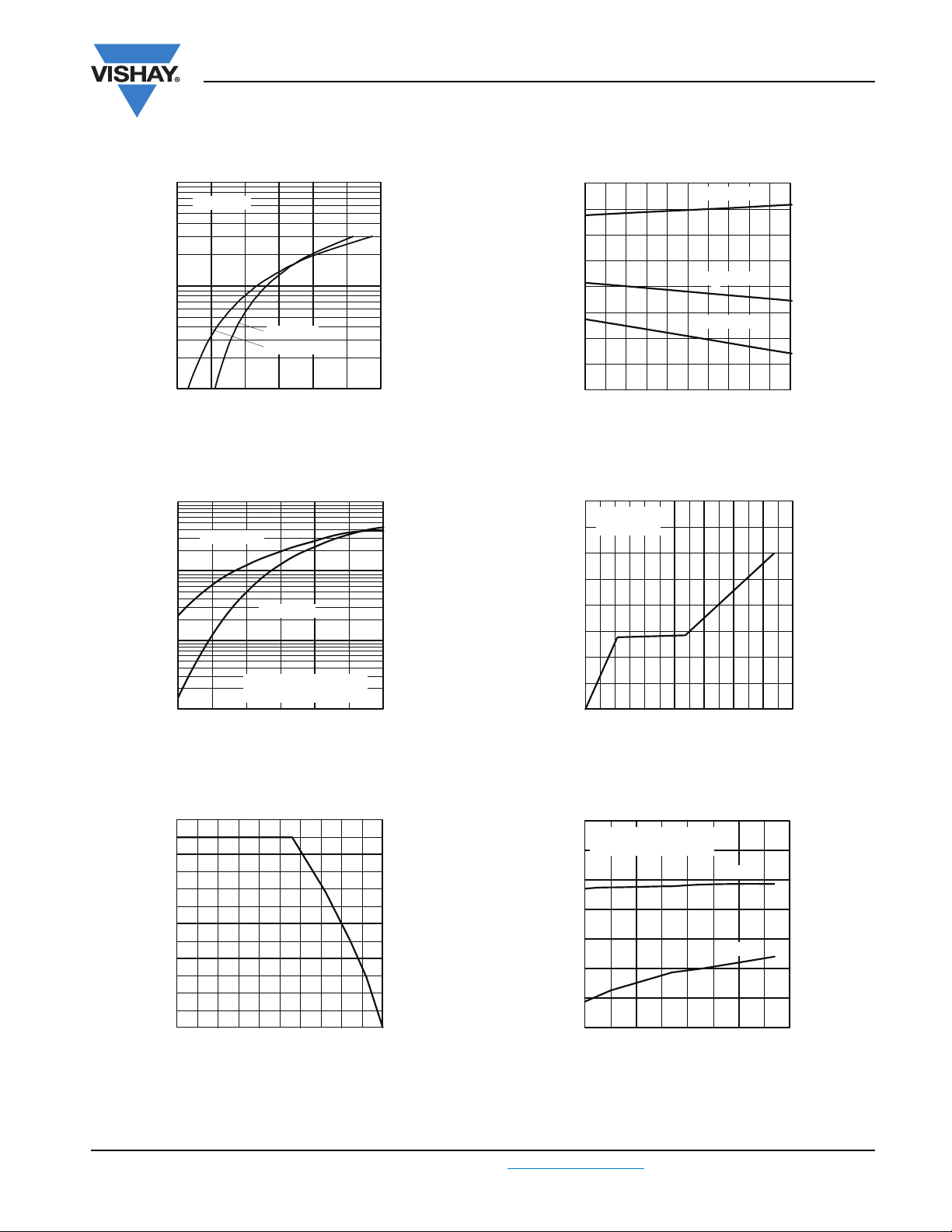
Fig. 1 - Typical Output Characteristics
1000
T = 125˚C
J
100
Tj = 125˚C
Vishay High Power Products
1.5
1.3
1.1
0.9
, Collector-to-Emitter Voltage (V)
CE
V
0.7
25 50 75 100 125 150
TJ, Junction Temperature (°C)
Fig. 4 - Typical Collector to Emitter Voltage vs.
Junction Temperature
20
Vcc = 400V
Ic = 100A
15
I = 200A
C
I = 100A
C
I = 50A
T = 25˚C
J
10
, Collector-to-Emitter Current (A)
C
I
Vce = 10V
380μs PULSE WIDTH
1
5.5 6.5 7.5 8.5
VGE, Gate-to-Emitter Voltage (V)
Fig. 2 - Typical Transfer Characteristics
240
200
160
120
80
40
Maximum DC Collector Current (A)
0
25 50 75 100 125 150
TC, Case Temperature (°C)
10
, Gate-to-Emitter Voltage (V)
5
GE
V
0
0 100 200 300 400 500 600 700
QG, Total Gate Charge (nC)
Fig. 5 - Typical Gate Charge vs.
Gate to Emitter Voltage
35
Tj = 25˚C, Vce = 480V
Vge = 15V, Ic = 100A
30
25
Eoff
20
15
10
Switching Losses (mJ)
Eon
5
0
10 20 30 40 50
RG, Gate Reistance (Ω)
Fig. 3 - Maximum Collector Current vs.
Case Temperature
Fig. 6 - Typical Switching Losses vs.
Gate Resistance
Document Number: 94544 For technical questions, contact: [email protected]
www.vishay.com
Revision: 04-May-10 3
Page 4
GA100TS60SFPbF
Vishay High Power Products
60
Tj = 125˚C
Vce = 480V
50
Vge = 15V
Ω
Rge = 15
40
30
20
Switching Losses (mJ)
10
0
04080120160
IC, Collector-to-Emitter Current (A)
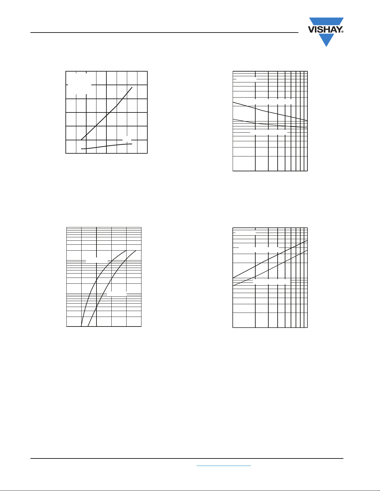
Fig. 7 - Typical Switching Losses vs.
Collector to Emitter Current
Eoff
Eon
"Half-Bridge" IGBT INT-A-PAK
(Standard Speed IGBT), 100 A
1000
Vr = 200V
100
(ns)
rr
t
10
Fig. 9 - Typical Reverse Recovery Time vs. dI
If = 50A, Tj = 125˚C
If = 50A, Tj = 25˚C
dif/dt - A/μs
0001001
/dt
F
1000
(A)
F
100
10
Instantaneous Forward Current - I
1
0 0.5 1 1.5 2 2.5
Tj = 125˚C
Tj = 25˚C
Forward Voltage Drop- VFM (V)
Fig. 8 - Maximum Forward Voltage Drop vs.
Instantaneous Forward Current
100
Vr = 200V
If = 50A, Tj = 125˚C
(A)
10
RRM
I
1
If = 50A, Tj = 25˚C
0001001
dif/dt - A/μs
Fig. 10 - Typical Reverse Recovery Current vs. dI
/dt
F
www.vishay.com For technical questions, contact: [email protected]
Document Number: 94544
4 Revision: 04-May-10
Page 5
GA100TS60SFPbF
"Half-Bridge" IGBT INT-A-PAK
(Standard Speed IGBT), 100 A
10000
(nC)
1000
RR
Q
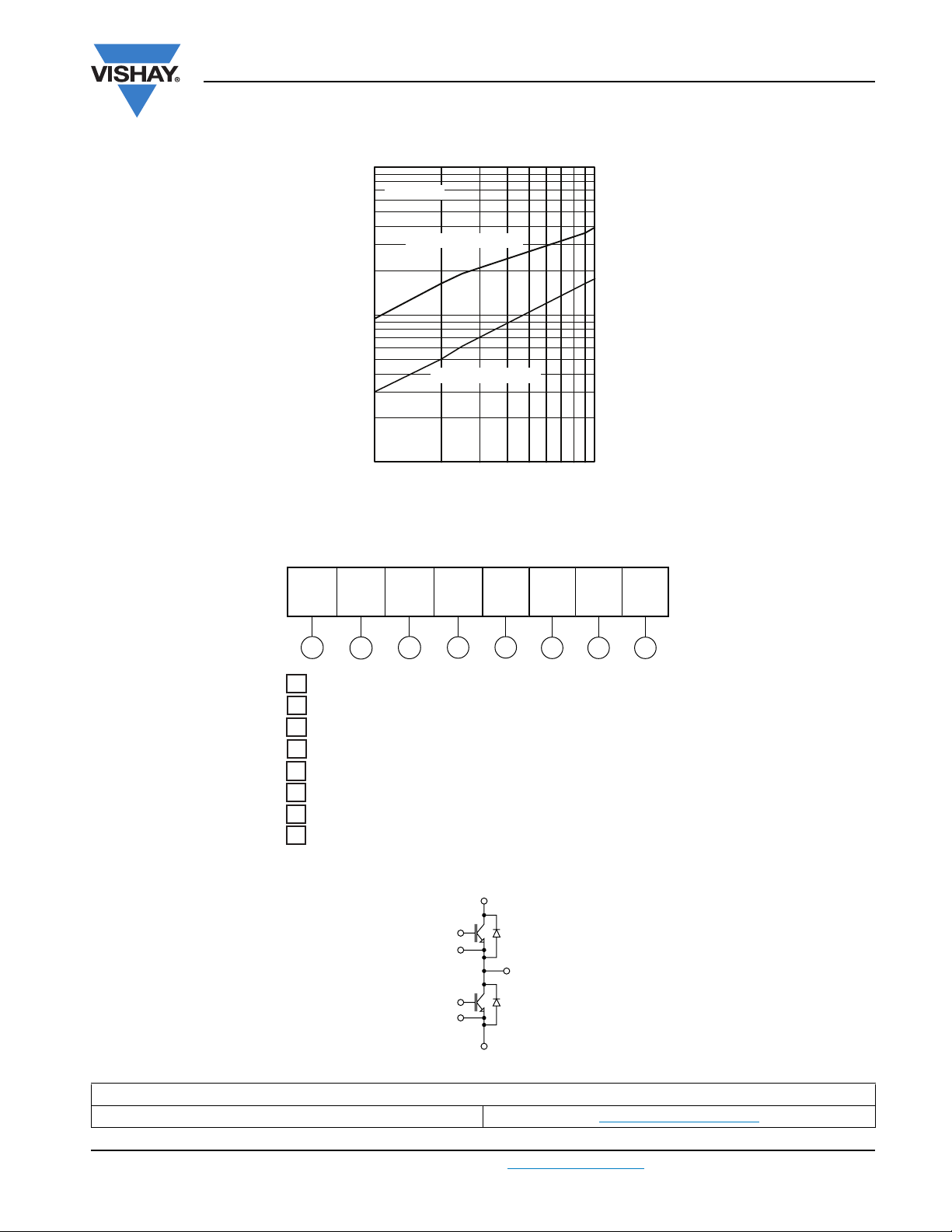
ORDERING INFORMATION TABLE
Vr = 200V
If = 50A, Tj = 125˚C
If = 50A, Tj = 25˚C
100
dif/dt - A/μs
Fig. 11 - Typical Stored Charge vs. dIF/dt
Vishay High Power Products
0001001
Device code
CIRCUIT CONFIGURATION
GA 100 T S 60 S F PbF
51324678
1 - Essential part number IGBT modules
2 - Current rating (100 = 100 A)
3
- Circuit configuration (T = Half bridge)
4 - INT-A-PAK
5 - Voltage code (60 = 600 V)
6 - Speed/type (S = Standard speed IGBT)
7 - Diode type
8 - PbF = Lead (Pb)-free
3
6
7
1
4
5
2
LINKS TO RELATED DOCUMENTS
Dimensions www.vishay.com/doc?95173
www.vishay.com
Page 6
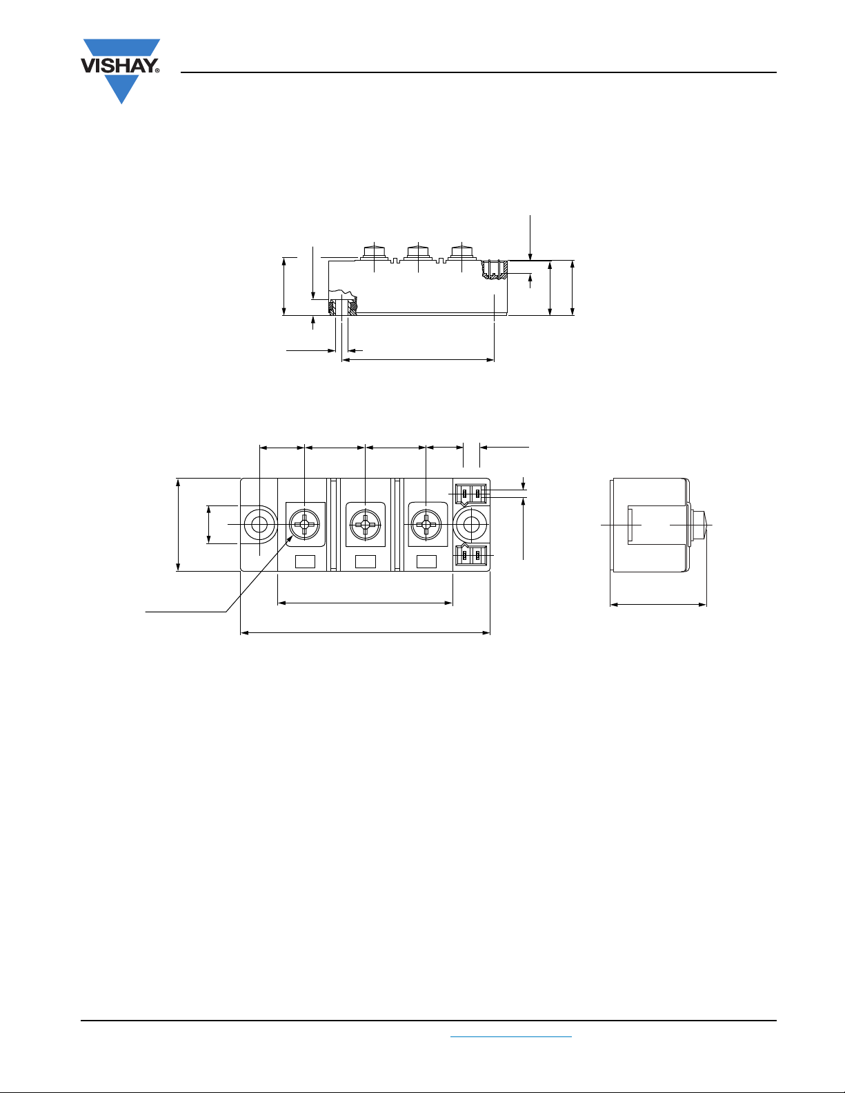
DIMENSIONS in millimeters (inches)
17 (0.67)
23 (0.91)
5 (0.20)
23 (0.91)
14.3
(0.56)
3 screws M6 x 10
66 (2.60)
94 (3.70)
35 (1.38)
14.5
(0.57)
1
2
3
2.8 x 0.8
(0.11 x 0.03)
5
4
7
6
37 (1.44)
80 (3.15)
Ø 6.5
(Ø 0.25)
30
(1.18)
9 (0.33)
7 (0.28)
28 (1.10)
29 (1.15)
Outline Dimensions
Vishay Semiconductors
INT-A-PAK IGBT
www.vishay.com
Page 7

Legal Disclaimer Notice
Vishay
Disclaimer
ALL PRODUCT, PRODUCT SPECIFICATIONS AND DATA ARE SUBJECT TO CHANGE WITHOUT NOTICE TO IMPROVE
RELIABILITY, FUNCTION OR DESIGN OR OTHERWISE.
Vishay Intertechnology, Inc., its affiliates, agents, and employees, and all persons acting on its or their behalf (collectively,
“Vishay”), disclaim any and all liability for any errors, inaccuracies or incompleteness contained in any datasheet or in any other
disclosure relating to any product.
Vishay makes no warranty, representation or guarantee regarding the suitability of the products for any particular purpose or
the continuing production of any product. To the maximum extent permitted by applicable law, Vishay disclaims (i) any and all
liability arising out of the application or use of any product, (ii) any and all liability, including without limitation special,
consequential or incidental damages, and (iii) any and all implied warranties, including warranties of fitness for particular
purpose, non-infringement and merchantability.
Statements regarding the suitability of products for certain types of applications are based on Vishay’s knowledge of typical
requirements that are often placed on Vishay products in generic applications. Such statements are not binding statements
about the suitability of products for a particular application. It is the customer’s responsibility to validate that a particular
product with the properties described in the product specification is suitable for use in a particular application. Parameters
provided in datasheets and/or specifications may vary in different applications and performance may vary over time. All
operating parameters, including typical parameters, must be validated for each customer application by the customer’s
technical experts. Product specifications do not expand or otherwise modify Vishay’s terms and conditions of purchase,
including but not limited to the warranty expressed therein.
Except as expressly indicated in writing, Vishay products are not designed for use in medical, life-saving, or life-sustaining
applications or for any other application in which the failure of the Vishay product could result in personal injury or death.
Customers using or selling Vishay products not expressly indicated for use in such applications do so at their own risk and agree
to fully indemnify and hold Vishay and its distributors harmless from and against any and all claims, liabilities, expenses and
damages arising or resulting in connection with such use or sale, including attorneys fees, even if such claim alleges that Vishay
or its distributor was negligent regarding the design or manufacture of the part. Please contact authorized Vishay personnel to
obtain written terms and conditions regarding products designed for such applications.
No license, express or implied, by estoppel or otherwise, to any intellectual property rights is granted by this document or by
any conduct of Vishay. Product names and markings noted herein may be trademarks of their respective owners.
Document Number: 91000 www.vishay.com
Revision: 11-Mar-11 1
 Loading...