

Page 1
Global Mixed-mode Technology Inc.
G9611
Low-Dropout, 300mA Linear Regulator with Reset
Features
300mA Output Current, with Foldback Current
Limiting
High Ripple Rejection
1.5% Output Accuracy
±±±±
2% Reset Threshold Accuracy
±±±±
Externally Programmable Reset Time Delay
Generator
Internal 300mA P-Channel Pass Transistor
320µA quiescent Current
Thermal Overload Protection
SOP 8 Package
Applications
CD ROM or DVD ROM
Slim-Type CD/DVD
DVD Player
General Description
The G9611 are low-dropout, linear regulator with
reset function supply 3.4V, 3.3V or 2.5V output for
currents up to 300mA. They are available in a
700mW SOP 8 package. Typical dropouts are
320mV at 300mA. Shutdown turns off linear regulator function. Other features include foldback current
limiting and thermal overload protection.
The reset function in G9611 detect V
hysteresis, keeping it asserted for time delay determined by external capacitor. The reset output is active low open-drain output. The detection threshold
are 3.9V or 4.2V.
The output is preset at 3.4V for the G9611A, 3.3V
for the G9611B/C, and 2.5V for G9611D. The reset
threshold is preset at 4.2V for G9611 A/B/D and
3.9V for G9611C.
level with
CC
Ordering Information
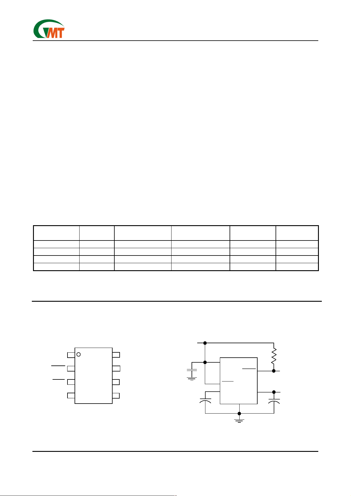
PART
NUMBER
G9611AP1x G9611A 3.4 4.2 -40°C to +85°C SOP 8L
G9611BP1x G9611B 3.3 4.2 -40°C to +85°C SOP 8L
G9611CP1x G9611C 3.3 3.9 -40°C to +85°C SOP 8L
G9611DP1x G9611D 2.5 4.2 -40°C to +85°C SOP 8L
MARKING
REGULATOR
OUTPUT VOLTAGE
Note: X Specify the packing type
U: Tape & Reel T: Tube
Pin configuration
RESET THRESHOLD
VOLTAGE
TEMP.
RANGE
Typical Operation Circuit
PIN-
PACKAGE
V
V
CC
CC
R
R
pull-high
pull-high
Ω
Ω
10k
10k
V
V
IN
1µF
1µF
IN
SHDN
SHDN
C
C
D
D
G9611
G9611
GND
GND
RESET
RESET
V
V
OUT
OUT
OUTPUT
OUTPUT
VOLTAGE
VOLTAGE
10µF
10µF
(Tantalum or Aluminum)
(Tantalum or Aluminum)
N.C
N.C
RESET
RESET
SHDN
SHDN
V
V
G9611
G9611
8
C
8
1
1
2
2
3
3
4
4
IN
IN
8Pin SOP
8Pin SOP
C
D
D
GND
7
GND
7
N.C
N.C
6
6
5
5
V
V
OUT
OUT
Ver: 1.2
Feb 13, 2003
TEL: 886-3-5788833
http://www.gmt.com.tw
1
Page 2
Global Mixed-mode Technology Inc.
G9611
Absolute Maximum Ratings
Supply Voltage (IN or OUT to GND……..-0.3V to +6.5V
Output Short-Circuit Duration…………….…………1 min
Input Voltage …………………..…-0.3V to the greater of
(IN+0.3V) or (OUT + 0.3V)
Continuous Power Dissipation (T
Stresses beyond those listed under "Absolute Maximum Ratings" may cause permanent damage to the device. These are stress rat-
ings only, and functional operation of the device at these or any other conditions beyond those indicated in the operational sections of
the specifications is not implied. Exposure to absolute maximum rating conditions for extended periods may affect device reliability
= +25°C)…...700mW
A
Operating Temperature Range……..…. -40°C to +85°C
Junction Temperature……………….……………+160°C
Storage Temperature Range…..…..….-65°C to +160°C
Lead Temperature (soldering, 10sec)…...….…..+300°C
Electrical Characteristics
VIN=5V, CIN=1µF, C
regulators are at V
PARAMETER SYMBOL CONDITIONS MIN TYP MAX UNITS
Input Voltage VIN 2.5 6.0 V
Output Voltage (Note 1) V
Load Regulation
Line Regulation
Dropout Voltage (Note 2)
Parameter Tempco V
Ripple Rejection PSRR
Output Noise en 20Hz to 100kHz, I
Quiescent Current IQ 320 450 µA
OFF Quiescent Current I
Foldback Current Limit I
Foldback Voltage V
Thermal Shutdown Temperature TSD 160 °C
Thermal Shutdown Hysteresis
SHDN Pin Input High Threshold
SHDN Pin Input Low Threshold
Reset Threshold V
Reset Threshold Hysteresis V
Reset Threshold Tempco 40 ppm/°C
CD Delay Pin Threshold Voltage V
CD Pin Sink Current ICD VCC=1.5V, VCD=0.5V 3 4.3 mA
CD Pin Pullup Resistance RD 100 200 400 kΩ
RESET Output Current Low IOL
RESET Function Operating Voltage VOP
Note 1: (VIN-V
OUT
limits.
Note 2: Dropout Voltage is (V
example, the G9611 is tested by measuring the V
100mV below the measured value. The difference (V
Note 3: Low duty pulse techniques are used during test to maintain junction temperature as close to ambient as possible.
=10µF, SHDN =VIN, TJ =TA=25°C (Note3), unless otherwise noted. Typical values for
OUT
=5V.
IN
G9611A 3.35 3.4 3.45
G9611B/C 3.25 3.3 3.35
OUT
V
G9611D 2.45 2.5 2.55
V
I
∆
LDR
V
∆
LNR
VDO I
∆
40 ppm/°C
OUT
QOFF
LIM
FOLDBACK
TSD 30 °C
∆
V
IH_
SHDN
V
IL_
SHDN
TH-
HYS
TCD
) is limited to keep the product (I
- V
IN
) when V
OUT
=1mA to 300mA, VIN=V
OUT
(V
+0.5V) ≤ V
OUT
=300mA 320 400 mV
OUT
f=120HZ, I
f=120HZ, I
SHDN
V
OUT<VFOLDBACK
V
OUT>VFOLDBACK
0.4V
≤
OUT
OUT
6V, I
≤
IN
=30mA 70
=300mA 65
=30mA. 350
OUT
260 400 580
650 900 1200
0.6 0.78 0.95 V
1.8 2 2.3 V
0.6 0.8 1.1 V
G9611A/B/D 4.11 4.2 4.29
G9611C 3.81 3.9 3.99
G9611A/B/D 150
G9611C 130
VCC = 5V 3.5 3.9 4.3 V
V
=2.5V, V
CC
RESET
sink current>10µA
x (VIN - V
OUT
falls to 100mV below its nominal value at VIN = V
OUT
RESET
OUT
=0.4V
OUT
at VIN = V
- V
IN
+1V 6 15 mV
OUT
=25mA -8 0.3 8 mV
OUT
dB
µVRMS
140 200 µA
mA
V
mV
8 11.5 mA
0.7 0.85 V
)) from exceeding the package power dissipation
+1V. For
OUT
+1V, then VIN is lowered until V
OUT
) is then measured and defined as ∆VDO.
OUT
OUT
falls
Ver: 1.2
Feb 13, 2003
TEL: 886-3-5788833
http://www.gmt.com.tw
2
Page 3
Global Mixed-mode Technology Inc.
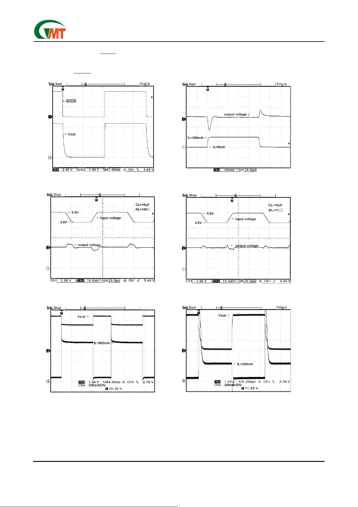
Typical Performance Characteristics
(VIN=5V,CIN=C
=10µF, SHDN =VIN, TJ=25°C, unless otherwise noted)
OUT
SHDN Pin vs. Output
Line Transient Line Transient
Load transient
G9611
Ver: 1.2
Feb 13, 2003
Over Current Response Short Circuit Response
3
TEL: 886-3-5788833
http://www.gmt.com.tw
Page 4

Global Mixed-mode Technology Inc.
Typical Performance Characteristics
Power Supply Rejection Ratio Power Supply Rejection Ratio
Power Supply Rejection Ratio
(continued)
0.305
0.3
0.295
0.29
0.285
0.28
0.275
0.27
Load Current (A)
0.265
0.26
0.255
G9611
Safe Operating Area of G9611 SO-8
TA=25°C
0.5 0.7 0.9 1.1 1.3 1.5 1.7 1.9 2.1 2.3 2.5 2.7
Input -Output Voltage Differential(V)
Ver: 1.2
Feb 13, 2003
4
TEL: 886-3-5788833
http://www.gmt.com.tw
Page 5

Global Mixed-mode Technology Inc.
Pin Description
PIN NO. PIN NAME PIN FUNCTION
1, 6 N.C No Connection.
2
3
4 VIN Regulator Input. Supply voltage can range from 2.5V to 6V.
5 V
7 GND Ground
8 CD External Programmable time delay is set by the capacitor connect to CD pin.
SHUTDOW N
SHDN
SHDN
SHUTDOW N
LOGIC
LOGIC
THERMAL
THERMAL
PROTECTION
PROTECTION
RESET
SHDN
Regulator Output. Sources up to 300mA.
OUT
-
-
+
+
1.24V
1.24V
REFERENCE
REFERENCE
RESET
Open-Drain Output remains low while VIN is below the reset threshold,
and for delay time set by C
SHDN
= High to enable regulator output.
SHDN
= Low to shutdown regulator output.
V
V
IN
IN
MOSFET D RIVER
MOSFET D RIVER
WITH FOLDBACK
WITH FOLDBACK
CURRENT LIMIT
CURRENT LIMIT
D
after VIN rises above the reset threshold.
P
P
V
V
OUT
OUT
R1
R1
G9611
RESET
RESET
-
-
+
+
R
R
D
D
C
C
D
D
Figure 1. Functional Diagram
Detailed Description
The G9611 are low-dropout, low-quiescent current
linear regulators with reset function The regulator in
G9611 supply 3.4V, 3.3V or 2.5V output for load currents up to 300mA. The reset function detect V
illustrated in Figure 1, they consist of a 1.24V reference, error amplifier, MOSFET driver, P-channel pass
transistor, and internal feedback voltage divider, reset
threshold comparator and time delay generator.
The 1.24V bandgap reference is connected to the error amplifier’s inverting input. The error amplifier compares this reference with the feedback voltage and
amplifies the difference. The MOSFET driver reads the
error signal and applies the appropriate drive to the
P-channel pass transistor. If the feedback voltage is
lower than the reference, the pass transistor gate is
pulled lower, allowing more current to pass and increasing the output voltage. If the feedback voltage is
too high, the pass transistor gate is pulled up, allowing
less current to pass to the output.
IN.
As
R2
R2
GND
GND
The G9611 also offer reset function to detect the level
of V
. They assert a reset signal whenever VIN supply
IN
voltage declines below a preset threshold (V
), keep-
TH
ing it asserted for time delay set by capacitor connected to C
reset threshold (V
pin, after VIN has resen above the high
D
+ V
TH
HYS
). The
RESET
is an active
low, open-drain output.
Internal P-Channel Pass Transistor
The G9611 feature a 300mA P-channel MOSFET
pass transistor. This provides several advantages over
similar designs using PNP pass transistors, including
longer battery life. The P-channel MOSFET requires
no base drive, which reduces quiescent current considerably. PNP based regulators waste considerable
amounts of current in dropout when the pass transistor
saturates. They also use high base-drive currents under large loads. The G9611 do not suffer from these
problems and consume only 320µA of quiescent current.
Additional blocks of linear regulator include a foldback
current limiter, thermal sensor, and shutdown logic.
Ver: 1.2
Feb 13, 2003
TEL: 886-3-5788833
http://www.gmt.com.tw
5
Page 6

Global Mixed-mode Technology Inc.
Shutdown
A low input on the SHDN pin shuts down the G9611.
In the off mode, the pass transistor, regulator control
circuit are turned off, Only reset function is turned on,
reducing the supply current below 140µA.
should be connected to V
for normal operation.
IN
Use a fast comparator, Schmitt trigger, or CMOS or
TTL Logic to drive the
SHDN pin in and out of shut-
down. Rise times should be shorter than 1µs. Do not
use slow RC circuits, leave
input to linger between thresholds.
SHDN open, or allow the
Foldback Current Limiting
The G9611 also include a foldback current limiter. It
monitors and controls the pass transistor’s gate voltage, estimating the output current and limiting it to
900mA for output voltages above 0.78V. If the output
voltage drops below 0.78V, implying a short-circuit
condition, the output current is limited to 400mA.
Thermal Overload Protection
Thermal overload protection limits total power dissipation in the G9611. When the junction temperature exceeds T
to the shutdown logic, turning off the pass transistor
and allowing the IC to cool. The thermal sensor will
turn the pass transistor on again after the IC’s junction
temperature cools by 30°C, resulting in a pulsed output during thermal overload conditions.
Thermal overload protection is designed to protect the
G9611 in the event of fault conditions. For continual
operation, the absolute maximum junction temperature
rating of T
Operating Region and Power Dissipation
Maximum power dissipation of the G9611 depends on
the thermal resistance of the case and circuit board,
the temperature difference between the die junction
and ambient air, and the rate of air flow. The power
dissipation across the device is P = I
The resulting maximum power dissipation is:
where (T
the G9611 die junction and the surrounding air,
the thermal resistance of the package chosen, and
is the thermal resistance through the printed circuit
board, copper traces and other materials to the sur-
= +160°C, the thermal sensor sends a signal
J
= +160°C should not be exceeded.
J
OUT
(T
)
P
=
MAX
J-TA
+
θ
CA
)
(
θ
JC
) is the temperature difference between
J -TA
SHDN
(VIN-V
θ
OUT
JC
θ
is
CA
G9611
rounding air. The thermal resistance of SOP-8 is
= 192°C/W .
The power dissipation of G9611 is:
P
= (V
- V
) x I
D
IN
OUT
The worst-case thermal resistance from case to air
(
) requirements are:
θ
CA
(125°C -T
=
θ
CA
P
Use larger copper pad area to obtain specific heat sink
thermal resistance values for larger output current,
higher input-output difference, and higher ambient
temperature.
C
Capacitor Selection
D
The reset timeout delay is set by internally pull-up R
(typical value 200kΩ) and external C
When the voltage at C
old, typically 0.85 V
voltage detector and buffer have built-in hysterisis to
prevent erratic reset operation. For C
reset time delay is 10ms.
Regulator Output Capacitor Selection and Regulator Stability
Normally, use capacitors 0.1µF minimum on the input
and 10µF minimum on the output of the G9611. The
larger input capacitor values provide better supply noise
rejection and line-transient response. Improve load transient response, stability, and power-supply rejection by
using large output capacitors. For stable operation over
the full temperature range and with load current up to
300mA, 10µF tantalum or 47µF aluminum minimum is
recommended. Too small capacitors with small ESR
can result in oscillation.
Transient Considerations
The
).
Typical Operating Characteristics
G9611 load-transient response. Two components of
the output response can be observed on the
load-transient graphs—a DC shift from the output impedance due to the different load currents, and the
transient response. Typical transients for step
changes in the load current from 5mA to 500mA are
0.1V. Increasing the output capacitor’s value attenuates transient spikes.
OUT
)
A
D
.
D
pin exceeds the buffer thresh-
D
, the
CC
RESET
output high. The
= 0.1µF, typical
D
θ
JC
D
show the
Ver: 1.2
Feb 13, 2003
6
TEL: 886-3-5788833
http://www.gmt.com.tw
Page 7

Global Mixed-mode Technology Inc.
Package Information
G9611
C
E
H
L
D
θ
7
(4X)
°
A2
A
y
Note:
1. Package body sizes exclude mold flash and gate burrs
2. Dimension L is measured in gage plane
3. Tolerance 0.10mm unless otherwise specified
Controlling dimension is millimeter converted inch dimensions are not necessarily exact.
4.
e
B
SYMBOL
A 1.35 1.60 1.75 0.053 0.063 0.069
A1 0.10 ----- 0.25 0.004 ----- 0.010
A2 ----- 1.45 ----- ----- 0.057 -----
B 0.33 ----- 0.51 0.013 ----- 0.020
C 0.19 ----- 0.25 0.007 ----- 0.010
D 4.80 ----- 5.00 0.189 ----- 0.197
E 3.80 ----- 4.00 0.150 ----- 0.157
e ----- 1.27 ----- ----- 0.050 -----
H 5.80 ----- 6.20 0.228 ----- 0.244
L 0.40 ----- 1.27 0.016 ----- 0.050
y ----- ----- 0.10 ----- ----- 0.004
θ
MIN. NOM. MAX. MIN. NOM. MAX.
0º ----- 8º 0º ----- 8º
DIMENSION IN MM DIMENSION IN INCH
A1
Taping Specification
Feed Direction
Feed Direction
Typical SOP Package Orientation
Typical SOP Package Orientation
GMT Inc. d oes not assume any responsibility for use of any circuitry described, no circuit patent licenses are implied and GMT Inc. reserves the right at any time without notice to change said circuitry and specifications.
Ver: 1.2
Feb 13, 2003
7
TEL: 886-3-5788833
http://www.gmt.com.tw
 Loading...