

Page 1
Ver: 1.6
Nov 18, 2002
TEL: 886-3-5788833
http://www.gmt.com.tw
1
G960
Global Mixed-mode Technology Inc.
3.3V 1A Low Dropout Regulator
Features
Dropout voltage typically 0.8V @ IO = 1A
Output current in excess of 1A
Output voltage accuracy ±2%
Quiescent current, typically 600µA
Internal short circuit current limit
Internal over temperature protection
Applications
CD-R/W
ADSL
Cable Modem
Set-Top-Box
LAN switch/Hub
Router
DVD-R/W
General Description
The G960 positive 3.3V voltage regulator features
the ability to source 1A of output current with a
dropout voltage of typically 0.8V over the entire operating temperature range. A low quiescent current
is provided over the entire current output current
range. The typical quiescent current is 0.6mA. Furthermore, the quiescent current is smaller when the
regulator is in the dropout mode (V
IN
< 3.3V).
Familiar regulator features such as over temperature and over current protection circuits are provided to prevent it from being damaged by abnormal operating conditions.
Ordering Information
PIN OPTION
ORDER NUMBER PACKAGE TYPE
1 2 3
G960T33T TO220 GND V
OUT
V
IN
G960T36T TO220 V
IN
V
OUT
GND
G960T43U TO252 GND V
OUT
V
IN
G960T45U TO252 V
IN
GND V
OUT
G960T53U TO263 GND V
OUT
V
IN
G960T63U SOT223 GND V
OUT
V
IN
Order Number Identification
GXXX XX X X
Packing Type
Pin Option
Package Type
Part Number
PACKAGE TYPE PIN OPTION PACKING
T3 : TO 220
1 2 3
U & D : Tape & Reel Direction
T4 : TO 252 1 : V
OUT
GND VIN T : Tube
T5 : TO 263 2 : V
OUT
VIN GND
T6 : SOT 223 3 : GND V
OUT
VIN
4 : GND V
IN
V
OUT
5 : V
IN
GND V
OUT
6 : V
IN
V
OUT
GND
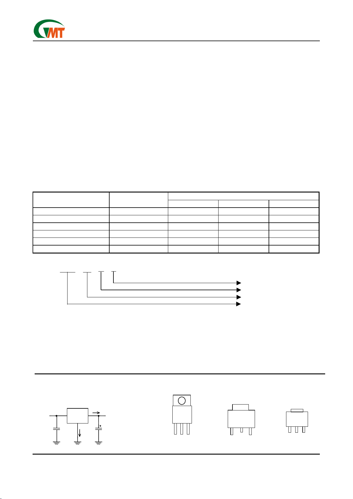
Typical Application Package Type
[Note 4] : Type of C
OUT
G960
C1
0.47µF
IQ
V
IN
V
OUT
I
O
C
OUT
10µF
1
3
TO 220
2
Top View
1
2
3
SOT 223
Top View
1
2
3
TO 252
、、、、
263
Top View
G960
C1
0.47µF
IQ
V
IN
V
OUT
I
O
C
OUT
10µF
1
3
TO 220
2
Top View
1
2
3
SOT 223
Top View
1
2
3
TO 252
、、、、
263
Top View
1
3
TO 220
2
Top ViewTop View
1
2
3
SOT 223
Top View
1
2
3
TO 252
、、、、
263
Top View
Page 2
Ver: 1.6
Nov 18, 2002
TEL: 886-3-5788833
http://www.gmt.com.tw
2
G960
Global Mixed-mode Technology Inc.
Absolute Maximum Ratings
(Note 1)
Input Voltage……………………….……………..……10V
Power Dissipation Internally Limited . (Note 2)
Maximum Junction Temperature.…..………………...150°C
Storage Temperature Range….…...-65°C ≤ T
J
≤+150°C
Lead Temperature, Time for Wave Soldering
TO 220, TO 263 Package…………..………..260°C, 10s
TO 252, SOT 223 Package……………………260°C, 4s
Continuous Power Dissipation (T
A
= +25°C)
SOT 223
(1)
………………………….………………....0.8W
TO 252
(1)
………………………….………………..….1.0W
TO 263
(1)
………………………….………………..….1.6W
TO 220
(1)
………………………….………………..….2.0W
Note
(1)
: See Recommended Minimum Footprint
Operating Conditions
(Note 1)
Input Voltage……………………………………….4V~7V
Temperature Range………….………-40°C ≤ T
J
≤125°C
Electrical Characteristics
VIN =5V, IO = 1A, CIN = 1µF, C
OUT
=10µF, All specifications apply for TA = TJ = 25°C. [Note 3]
PARAMETER CONDITIONS MIN TYP MAX UNITS
Output Voltage 50mA < IO <1A 3.234 3.3 3.366 V
Line Regulation 4V < VIN < 7V, IO = 10mA 20 30 mV
Load Regulation 50mA < IO < 1A 30 50 mV
Output Impedance 200mA DC and 100mA AC, fo = 120Hz 100
mΩ
Quiescent Current V
IN
= 5V 0.6 mA
Ripple Rejection fi = 120Hz, 1V
P-P,
Io = 100mA 42 dB
IO = 1A 0.8 V
Dropout Voltage
I
O
= 100mA 200 mV
Short Circuit Current 1.6 1.9 A
Over Temperature 125 °C
Note 1:
Absolute Maximum Ratings are limits beyond which damage to the device may occur. Operating
Conditions are conditions under which the device functions but the specifications might not be guaranteed. For
guaranteed specifications and test conditions see the Electrical Characteristics.
Note 2:
The maximum power dissipation is a function of the maximum junction temperature, T
Jmax
; total thermal resis-
tance,
θ
JA
, and ambient temperature TA. The maximum allowable power dissipation at any ambient temperature
is T
jmax-TA
/
θ
JA
. If this dissipation is exceeded, the die temperature will rise above 150°C and IC will go into ther-
mal shutdown. For the G960 in the SOT 223 package,
θ
JA
is 156°C/W; in the TO 252 package,
θ
JA
is 125°C/W;
in the TO 263 package,
θ
JA
is 75°C/W, and in the TO 220 package,
θ
JA
is 60°C/W (No heat sink). [See Recom-
mended Minimum Footprint] If the TO 220 package is used with a heat sink,
θ
JA
is the sum of the package
thermal resistance junction-to-case (
θ
JC
) of 3°C/W and the thermal resistance added by the heat sink and thermal interface the thermal resistance can be reduced by increasing the P.C. board copper area thermally connected to the package. The safe operation area of SOT 223, TO 252, TO 263 or TO 220 package, it can see
“Typical Performance Characteristics” (Safe Operating Area).
Note3:
Low duty pulse techniques are used during test to maintain junction temperature as close to ambient as possible.
Note4:
The type of output capacitor should be tantalum or aluminum.
Definitions
Dropout Voltage
The input/output Voltage differential at which the regulator output no longer maintains regulation against further reductions in input voltage. Measured when the
output drops 100mV below its nominal value, dropout
voltage is affected by junction temperature, load current and minimum input supply requirements.
Line Regulation
The change in output voltage for a change in input
voltage. The measurement is made under conditions of
low dissipation or by using pulse techniques such that
average chip temperature is not significantly affected.
Load Regulation
The change in output voltage for a change in load
current at constant chip temperature. The measurement is made under conditions of low dissipation or
by using pulse techniques such that average chip
temperature is not significantly affected.
Maximum Power Dissipation
The maximum total device dissipation for which the
regulator will operate within specifications.
Quiescent Bias Current
Current which is used to operate the regulator chip
and is not delivered to the load.
Page 3
Ver: 1.6
Nov 18, 2002
TEL: 886-3-5788833
http://www.gmt.com.tw
3
G960
Global Mixed-mode Technology Inc.
Typical Performance Characteristics
(VIN=5V, CIN=1µF, C
OUT
=10µF, TA=25°C, unless otherwise noted.)
0
200
400
600
800
1000
1200
0 100 200 300 400 500 600 700 800 900 1000
Load Current (mA)
Dropout Voltage (mV)
3.260
3.280
3.300
3.320
3.340
3.360
3.380
0 100 200 300 400 500 600 700 800 900 1000
Load Current (mA)
Output Voltage (V)
0.4
0.6
0.8
1.0
1.2
1.4
1.6
1.8
2.0
2.2
0 100 200 300 400 500 600 700 800 900 1000
Load Current (mA)
Ground Current (mA)
Line Transient Load Transient
Ch1: Vout (offset =3.30V)
Ch2: Vin (offset=5 .0V)
Iout=100mA
Ch1: Vout (offset =3.30V)
Ch2: Iout (780mA/ div)
Output Voltage vs. Load Current Dropout Voltage vs. Load Current
Ground Current vs. Load Current
Page 4

Ver: 1.6
Nov 18, 2002
TEL: 886-3-5788833
http://www.gmt.com.tw
4
G960
Global Mixed-mode Technology Inc.
Typical Performance Characteristics
(continued)
0
100
200
300
400
500
600
700
800
900
1000
1100
1200
0.0 0.2 0.4 0.6 0.8 1.0 1.2 1.4 1.6 1.8 2.0 2.2 2.4 2.6 2.8 3.0 3.2
Input-Output Voltage Differen tial VIN-VOUT (V)
Output Current (mA)
TA=25
℃
TA=55
℃
TA=85
℃
1oz Copper on SOT 223
Package Mounted on
recommended mimimum
footpr int (R
θ
JA
=156°C/W)
Maximum recommended output current TA=25°C,Still Air
Note: V
IN(max)
<= 6.5V
0.0
0.1
0.2
0.3
0.4
0.5
0.6
0.7
0.8
0.9
1.0
25 35 45 55 65 75 85 95 105 115 125
Amibent Te mperature TA (°C)
Power Dissipation (W)
Still Air
1oz Copper on SOT 223
Package Mounted on
recommend mimimum
footprint (R
θ
JA
=156°C/W)
0.0
0.1
0.2
0.3
0.4
0.5
0.6
0.7
0.8
0.9
1.0
1.1
1.2
25 35 45 55 65 75 85 95 105 115 125
Amibent T emperature TA (°C)
Power Dissipation (W)
Still Air
1oz Copper on TO 252
Package Mounted on
recommend mimimum
footprint (R
θ
JA
=125°C/W)
0
100
200
300
400
500
600
700
800
900
1000
1100
1200
0.0 0.2 0.4 0.6 0.8 1.0 1.2 1.4 1.6 1.8 2.0 2.2 2.4 2.6 2.8 3.0 3.2
Input-Outpu t Voltaage Dif ferential VI N-VOUT (V)
Output Current (mA)
TA=25
℃
TA=55
℃
TA=85
℃
1oz Copper on TO 263
Package Mounted on
recommended mimimum
footprint (R
θ
JA
=75°C/W)
Maximum recommended output current TA=25°C,Still Air
0.0
0.2
0.4
0.6
0.8
1.0
1.2
1.4
1.6
1.8
25 35 45 55 65 75 85 95 105 115 125
Amibent T emperature TA (℃)
Power Dissipation (W)
Still Air
1oz Copper on TO 263
Package Mounted on
recommend mimimum
footprint (R
θ
JA
=75°C/W)
0
100
200
300
400
500
600
700
800
900
1000
1100
1200
0.0 0.2 0.4 0.6 0.8 1.0 1.2 1.4 1.6 1.8 2.0 2.2 2.4 2.6 2.8 3.0 3.2
Input-Outpu t Voltaage Dif ferential VI N-VOUT (V)
Output Current (mA)
TA=25
℃
TA=55
℃
TA=85
℃
Maximum recommended output current TA=25°C,Still Air
1oz Copper on TO 252
Package Mounted on
recommended
mimimum footprint
(
R
=125°C/W
)
Note: V
IN(max)
<= 6.5V
Safe Operating Area of SOT 223 Maximum Power Dissipation of SOT 223
Safe Operating Area of TO 252 Maximum Power Dissipation of TO 252
Maximum Power Dissipation of TO 263Safe Operating Area of TO 263
Note: V
IN(max)
<= 6.5V
Page 5

Ver: 1.6
Nov 18, 2002
TEL: 886-3-5788833
http://www.gmt.com.tw
5
G960
Global Mixed-mode Technology Inc.
Typical Performance Characteristics
(continued)
0
100
200
300
400
500
600
700
800
900
1000
1100
1200
0.0 0.2 0.4 0.6 0.8 1.0 1.2 1.4 1.6 1.8 2.0 2.2 2.4 2.6 2.8 3.0 3.2
Input-Output Voltaage Differential VIN-V
OUT
(V)
Output Current (mA)
TA=25
℃
TA=55
℃
TA=85
℃
Maximum recommended output current TA=25°C,Still Air
No Heat Sink
Mounted on TO 220 recommended
mimimum footprint, without heat s ink
(R
θ
JA
=60°C/W)
0.0
0.2
0.4
0.6
0.8
1.0
1.2
1.4
1.6
1.8
2.0
2.2
2.4
25 35 45 55 65 75 85 95 105 115 125
Amibent Temperature TA (°C)
Power Dissipation (W)
Maximum Power Dissipation of TO 220
No Heat Sink
Still Air
1oz Copper on TO 220 Package
Mounted on recommend mimimum
=
°
Safe Operating Area of TO 220
Note: V
IN(max)
<= 6.5V
Recommended Minimum Footprint
Page 6

Ver: 1.6
Nov 18, 2002
TEL: 886-3-5788833
http://www.gmt.com.tw
6
G960
Global Mixed-mode Technology Inc.
Package Information
TO-220 (T3) Package
MILLIMETERS INCHES
SYMBOLS
MIN MAX MIN MAX
A 4.318 4.826 0.170 0.190
A1 2.46 2.72 0.097 0.107
b 0.69 0.94 0.027 0.037
b1 1.143 1.397 0.045 0.055
C 0.304 0.460 0.012 0.018
D 3.429 3.683 0.135 0.145
D1 8.53 9.04 0.336 0.356
d 2.62 2.87 0.103 0.113
E 9.906 10.40 0.390 0.410
E1 2.84 5.13 0.112 0.202
e 2.29 2.79 0.090 0.110
e1 4.83 5.33 0.190 0.210
F 1.143 1.397 0.045 0.055
I 3.454 3.962 0.136 0.156
L 13.589 14.351 0.535 0.565
E
R
E1 E1
D
d
I
L
e
b
b1
e1
A
F
D1
C
A1
Page 7

Ver: 1.6
Nov 18, 2002
TEL: 886-3-5788833
http://www.gmt.com.tw
7
G960
Global Mixed-mode Technology Inc.
TO-252 (T4) Package
Notes:
1. Dimensioning and tolerancing per ansi y14.5m, 1982.
2.
Controlling dimension: inch
MILLIMETERS INCHES
SYMBOLS
MIN MAX MIN MAX
A 5.97 6.35 0.235 0.250
B 6.35 6.73 0.250 0.265
C 2.19 2.38 0.086 0.094
D 0.69 0.88 0.027 0.035
E 0.84 1.01 0.033 0.040
F 0.94 1.19 0.037 0.047
G 4.58BSC 0.180BSC
H 0.87 1.01 0.034 0.040
J 0.46 0.58 0.018 0.023
K 2.60 2.89 0.102 0.114
L 2.29BSC 0.090BSC
R 4.45 6.46 0.175 0.215
S 0.51 1.27 0.020 0.050
U 0.51 --- 0.020 ---
V 0.77 1.27 0.030 0.050
Z 3.51 --- 0.138 ---
R
B
V
A
K
S
12
3
F
L
D
G
4
2 PL
0.13 (0.005)
M
T
Z
E
C
T
SEATING
PLANE
U
J
H
Page 8

Ver: 1.6
Nov 18, 2002
TEL: 886-3-5788833
http://www.gmt.com.tw
8
G960
Global Mixed-mode Technology Inc.
TO-263 (T5) Package
MILLIMETERS INCHES
SYMBOLS
MIN MAX MIN MAX
A 4.30 4.70 0.169 0.185
A1 1.22 1.32 0.048 0.055
A2 2.45 2.69 0.104 0.106
b 0.69 0.94 0.027 0.037
b1 1.22 1.40 0.048 0.055
C 0.36 0.56 0.014 0.022
D 8.64 9.652 0.340 0.380
E 9.70 10.54 0.382 0.415
e 2.29 2.79 0.090 0.110
e1 4.83 5.33 0.190 0.210
H 14.60 15.78 0.575 0.625
L 4.70 5.84 0.185 0.230
L1 1.20 1.778 0.047 0.070
L2 2.24 2.84 0.088 0.111
L3 1.40MAX 0.055MAX
e
L3
D
H
e1
b1
b
E
A
A1
C
A2
L2
L
L1
Page 9

Ver: 1.6
Nov 18, 2002
TEL: 886-3-5788833
http://www.gmt.com.tw
9
G960
Global Mixed-mode Technology Inc.
SOT-223 (T6) Package
MILLIMETERS INCHES
SYMBOLS
MIN MAX MIN MAX
A 1.55 1.80 0.061 0.071
A1 0.02 0.12 0.0008 0.0047
B 0.60 0.80 0.024 0.031
B1 2.90 3.10 0.114 0.122
C 0.24 0.32 0.009 0.013
D 6.30 6.70 0.248 0.264
E 3.30 3.70 0.130 0.146
e 2.30 BSC 0.090 BSC
e1 4.60 BSC 0.181 BSC
H 6.70 7.30 0.264 0.287
L 0.90 MIN 0.036 MIN
L2 0.06 BSC 0.0024 BSC
α
0º 10º 0º 10º
Package Orientation
GMT Inc. d oes not assume any responsibility for use of any circuitry described, no circuit patent licenses are implied and GMT Inc. reserves the right at any time without notice to change said circuitry and specifications.
A
B
13°(4X)
A1
e1
e
E
B1
D
H
C
α
13°(4X)
L2
L
Feed Direction
SOT 223 Package Orientation
Feed Direction
TO252
、、、、
263 Package Orientation
Feed Direction
SOT 223 Package Orientation
Feed Direction
TO252
、、、、
263 Package Orientation
 Loading...