

Page 1
Global Mixed-mode Technology Inc.
150mA Low-Dropout Linear Regulators
Features
Low, 52µA Ground Current
Guaranteed 150mA Output Current
Dropout Voltage is 100mV @ 50mA Load
Over-Temperature Protection and Short-Circuit
Protection
Adjustable Mode: from 2.5V to 5.5V
Max. Supply Current in Shutdown Mode < 1µA
Low Output Noise is 170 µV
Applications
Notebook Computers
Cellular Phones
PDAs
Digital still Camera and Video Recorders
Hand-Held Devices
Bar Code Scanners
RMS
G914
General Description
The G914 is a low supply current, low dropout linear
regulator that comes in a space saving SOT23-5 package. The supply current at no-load is 52µA. In the
shutdown mode, the maximum supply current is less
than 1µA. Operating voltage range of the G914 is from
2.5V to 5.5V. The over-current protection limit is set at
370mA typical and 150mA minimum. An overtemperature protection circuit is built-in in the G914 to
prevent thermal overload. These power saving features make the G914 ideal for use in the battery-powered applications such as notebook computers, cellular phones, and PDA’s.
The G914 is a adjustable output version in a small
SOT 23-5 package.
Ordering Information
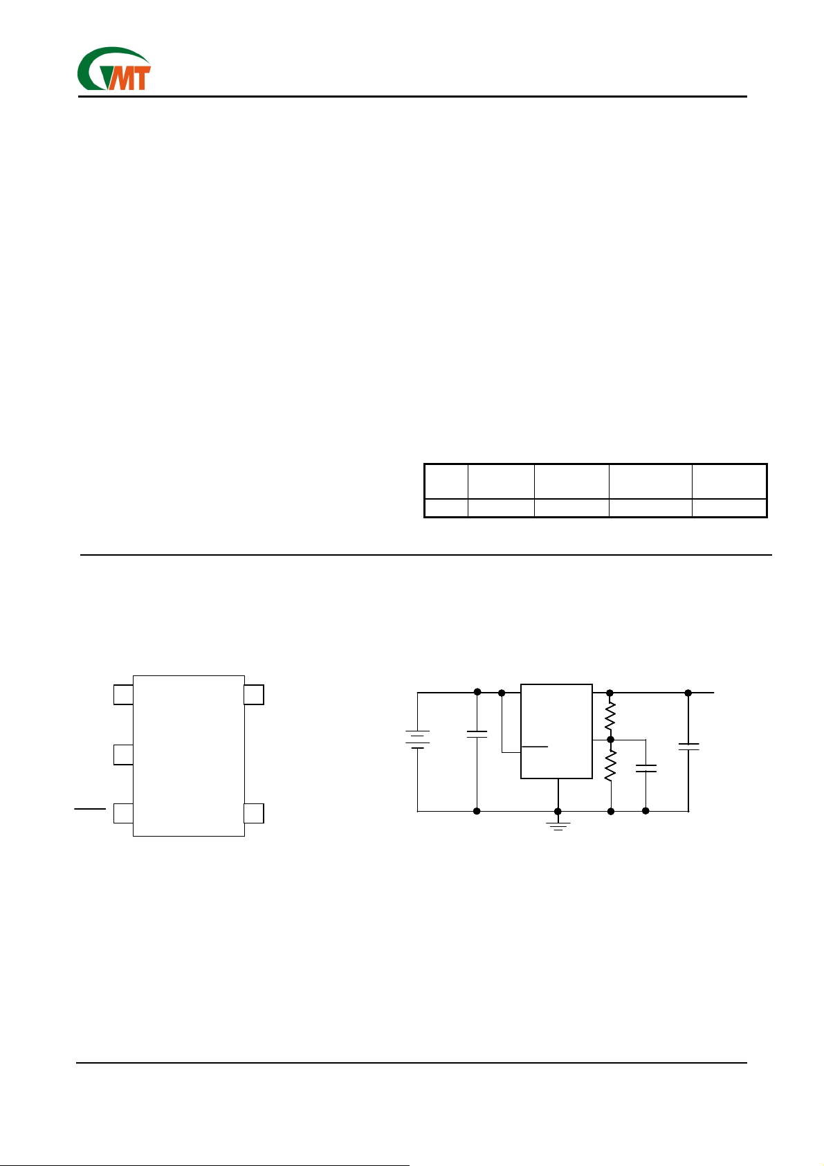
Pin Configuration
1
1
1
IN
IN
IN
2
2
2
GND
GND
GND
SHDN
SHDN
SHDN
3
3
3
G914
G914
G914
SOT23-5
SOT23-5
SOT23-5
PART MARKING VOLTAGE
TEMP.
RANGE
PIN-
PACKAGE
G914 14 Adjustable -40°C~ +85°C SOT 23-5
OUTPUT
OUTPUT
C
C
C
1µF
1µF
1µF
OUT
OUT
OUT
OUTPUT
VOLTAGE
VOLTAGE
VOLTAGE
OUT
OUT
G914
G914
G914
GND
GND
GND
OUT
ADJ
ADJ
ADJ
R1
R1
R1
R2
R2
R2
470pF
470pF
470pF
IN
IN
5
5
5
OUT
OUT
OUT
+
+
+
C
C
-
-
-
BATTERY
BATTERY
BATTERY
4
4
4
ADJ
ADJ
ADJ
V
V
V
OUT
OUT
OUT
C
1µF
1µF
1µF
=1.250 X ( R2/R1+1)
=1.250 X ( R2/R1+1)
=1.250 X ( R2/R1+1)
IN
SHDN
SHDN
SHDN
IN
IN
IN
Adjustable mode
Adjustable mode
Adjustable mode
Ver 0.2 Preliminary
Jul 19, 2002
1
TEL: 886-3-5788833
http://www.gmt.com.tw
Page 2
Absolute Maximum Ratings
VIN to GND……………………………………-0.3V to +7V
Output Short-Circuit Duration………………….….Infinite
SET to GND.……………………………..…..-0.3V to +7V
SHDN to GND…………………..………….-0.3V to +7V
SHDNto IN….…………………..…………..-7V to +0.3V
OUT to GND…………………………-0.3V to (V
Stresses beyond those li sted under "Absolute Maximum Ratings" may cause permanent damage to the device. These are stres s ratings only, and functional operat i on of the device at these or any other condit i ons beyond those indicated in the operational sections of
the specifications is not implied. Exposure to absolute maximum rating c ondi tions for extended periods may affect devi ce reliability.
Global Mixed-mode Technology Inc.
Continuous Power Dissipation (T
SOT23-5……………………………………...…..568 mW
Operating Temperature Range………...-40°C to +85°C
Junction Temperature……………………….……+150°C
….…..……………….…………….…..…..220°C/Watt
θ
JA
Storage Temperature Range………….-65°C to +160°C
Lead Temperature (soldering, 10sec)..…………+300°C
+ 0.3V)
IN
= +25°C)
A
G914
Electrical Characteristics
(V
= V
OUT
+1V;
IN
PARAMETER SYMBOL CONDITIONS MIN TYP MAX UNITS
Input Voltage (Note 2) VIN Note2 5.5 V
Output Voltage Accuracy V
Adjustable Output Voltage Range (Note 3) V
Maximum Output Current 150 mA
Current Limit I
Ground Pin Current IQ
Dropout Voltage (Note 3) V
Line Regulation
Load Regulation
Output Voltage Temperature Coefficient ∆VO / ∆T I
Output Voltage Noise (10HZ to 100KHZ) en IL = 150mA
SHUTDOWN
SHDN
Input Threshold
SHDN
Input Bias Current
Shutdown Supply Current I
ADJ INPUT
ADJ Input Leakage Current I
THERMAL PROTECTION
Thermal Shutdown Temperature T
Thermal Shutdown Hysteres is
Note 1: Limits is 100% production tested at T
maintain junction temperature as close to ambient as possible.
Note 2: V
IN (min)
= V
Note 3: The dropout voltage is defined as (V
= VIN; CIN = C
V
SHDN
+V
OUT
DROP
= 1µF = TA = TJ = +25°C, unless otherwise noted.) (Note 1)
OUT
Variation from specified V
OUT
2.5 5.5 V
OUT
V
LIM
DROP
V
VIN=VO +0.1V to 5.5V , I
∆
LNR
V
I
∆
LDR
= 0V 370 mA
OUT
I
= 0mA
LOAD
= 150mA
I
LOAD
I
= 1mA 2
OUT
I
= 50mA 100
OUT
I
=150mA 340
OUT
= 0mA to 150mA 8 25 mV
OUT
= 40mA, TJ = 25°C to 125°C 40 ppm/°C
OUT
VIH Regulator enabled 2
V
Regulator shutdown 0.4
IL
V
I
SHDN
V
QSHDN
V
ADJ
150 °C
SHDN
T
15 °C
∆
SHDN
= VIN
SHDN
= 0V TA = +25°C 0.06 1 µA
OUT
= 1.3V TA = +25°C 5 30 nA
ADJ
= +25°C. Low duty pulse techniques are used during test to
A
, I
OUT
=1mA -3 3 %
OUT
52 80 µA
= 1m A 0.1 %/V
OUT
C
= 470pF 192
ADJ
C
= 10nF 170
ADJ
T
= +25°C
A
0.007 0.1 µA
µV
mV
RMS
V
.
IN-VOUT
) when V
is 100mV below the value of V
OUT
for VIN = V
OUT
OUT
+2V.
Ver 0.2 Preliminary
Jul 19, 2002
2
TEL: 886-3-5788833
http://www.gmt.com.tw
Page 3

Global Mixed-mode Technology Inc.
Pin Description
NAME
PIN
1 IN Regulator Input. Supply vol tage can range from +2.5V to +5.5V. Bypass with 1µF to GND
2 GND
3
4 ADJ
5 OUT
SHDN
Ground. This pin als o functions as a heatsink . Solder to lar ge pads or the circui t board gr ound plane to
maximize thermal dissipation.
Active-Low Shutdown Input. A logic low reduces the supply current to less than 1µA. Connect to IN for normal
operation.
Adjust (Input): Adjustable regulator feedback input. It can connect to an external res istor divi der for adjustable output voltage. It also must connect ≥470pF ceramic capacit or from ADJ pin to GND for r educe
output noise.
Regulator Output. Fixed or adjus table from +2.5V to +5.5V. Sour ces up to 150mA. Bypass wit h a 1µF,
0.2Ω typical ESR capacit or to GND.
<
FUNCTION
G914
Detailed Description
The block diagram of the G914 is shown in Figure 1. It
consists of an error amplifier, 1.25V bandgap reference, PMOS output transistor, shutdown logic, over
current protection circuit, and over temperature protection circuit.
The G914 can be adjusted to a specific output voltage
by using two external resistors (Figure 2). The resistors set the output voltage based on the following
equation:
V
OUT
=1.250V X
R2
R1
+ 1
IN
IN
SHDN
SHDN
SHUTDOWN
SHUTDOWN
LOGIC
LOGIC
This equation is correct due to the configuration of the
bandgap reference. The bandgap voltage is relative to
the output, as seen in the block diagram. Traditional
regulators normally have the reference voltage relative
to ground and have a different V
equation. Resistor
OUT
values are not critical because ADJ (adjust)has a high
input impedance, but for best results use resistors of
470kΩ or less. A capacitor from ADJ to ground provides greatly improved noise performance.
ERROR
ERROR
AMP.
AMP.
+
+
GND
GND
Ver 0.2 Preliminary
Jul 19, 2002
OVER TEMP. &
OVER TEMP. &
OVER CURRENT
OVER CURRENT
PROTECTION
PROTECTION
1.25V
1.25V
ref
ref
Figure 1. Functional Diagram
3
OUT
OUT
ADJ
ADJ
TEL: 886-3-5788833
http://www.gmt.com.tw
Page 4

+
+
-
-
BATTERY
BATTERY
Over Current Protection
The G914 use a current mirror to monitor the output
current. A small portion of the PMOS output transistor’s current is mirrored onto a resistor such that the
voltage across this resistor is proportional to the output current. This voltage is compared against the reference voltage. Once the output current exceeds the
limit, the PMOS output transistor enters constant current mode. The current is set to 370mA typically.
Over Temperature Protection
To prevent abnormal temperature from occurring, the
G914 has a built-in temperature monitoring circuit.
When it detects the temperature is above 150
output transistor is turned off. W hen the IC is cooled
down to below 135
this way, the G914 will be protected against abnormal
junction temperature during operation.
Shutdown Mode
When the
the G914 enters shutdown mode. All the analog circuits are turned off completely, which reduces the
current consumption to only the leakage current. The
output is disconnected from the input. When the output has no load at all, the output voltage will be discharged to ground through the internal resistor voltage
divider.
Operating Region and Power Dissipation
Since the G914 is a linear regulator, its power dissipation is always given by P = I
maximum power dissipation is given by:
P
D(MAX)
Global Mixed-mode Technology Inc.
OUTPUT
OUT
OUT
OUTPUT
VOLTAGE
VOLTAGE
R
R
L
L
o
C, the
). The
OUT
OUT
OUT
IN
IN
R1
R1
R2
R2
470pF
470pF
C
C
1µF
1µF
C
C
1µF
1µF
G914
G914
ADJ
ADJ
SHDN
SHDN
IN
IN
GND
GND
Figure 2. Adjustable Output Using External
Feedback Resistors
o
C, the output is turned on again. In
pin is connected a logic low voltage,
SHDN
(VIN – V
OUT
= (TJ–TA)/
,=150oC-25oC/220oC/W= 568mW
θ
JA
G914
of the chosen package to the ambient air. In the case
of a SOT23-5 package, the thermal resistance is typically 220
The die attachment area of the G914’s lead frame is
connected to pin 2, which is the GND pin. Therefore,
the GND pin of G914 can carry away the heat of the
G914 die very effectively. To improve the power dissipation, connect the GND pin to ground using a large
ground plane near the GND pin.
Applications Information
Capacitor Selection and Regulator Stability
Normally, use a 1µF capacitor on the input and a 1µF
capacitor on the output of the G914. Larger input capacitor values and lower ESR provide better supply-noise rejection and transient response. A highervalue input capacitor (10µF) may be necessary if large,
fast transients are anticipated and the device is located several inches from the power source.
Power-Supply Rejection and Operation from Sources
Other than Batteries
The G914 is designed to deliver low dropout voltages
and low quiescent currents in battery powered systems. Power-supply rejection is 42dB at low frequencies.
When operating from sources other than batteries,
improve supply-noise rejection and transient response
by increasing the values of the input and output capacitors, and using passive filtering techniques.
Load Transient Considerations
The G914 load-transient response graphs show two
components of the output response: a DC shift of the
output voltage due to the different load currents, and
the transient response. Typical overshoot for step
changes in the load current from 0mA to 100mA is
12mV. Increasing the output capacitor's value and
decreasing its ESR attenuates transient spikes.
Input-Output (Dropout) Voltage
A regulator's minimum input-output voltage differential
(or dropout voltage) determines the lowest usable
supply voltage. In battery-powered systems, this will
determine the useful end-of-life battery voltage. Because the G914 use a P-channel MOSFET pass transistor, their dropout voltage is a function of R
multiplied by the load current.
o
C/Watt.
DS(ON)
Where (T
) is the temperature difference the G914
J–TA
die and the ambient air,
Ver 0.2 Preliminary
Jul 19, 2002
, is the thermal resistance
θ
JA
4
TEL: 886-3-5788833
http://www.gmt.com.tw
Page 5

Layout Guide
An input capacitance of ≅ 1µF is required between the
G914 input pin and ground (the amount of the capacitance may be increased without limit), This capacitor
must be located a distance of not more than 1cm from
the input and return to a clean analog ground.
Input capacitor can filter out the input voltage spike
caused by the surge current due to the inductive effec t
of the package pin and the printed circuit board’s
Global Mixed-mode Technology Inc.
G914
routing wire. Otherwise, the actual voltage at the IN
pin may exceed the absolute maximum rating.
The output capacitor also must be located a distance
of not more than 1cm from output to a clean analog
ground. Because it can filter out the output spike
caused by the surge current due to the inductive effec t
of the package pin and the printed circuit board’s
routing wire. Figure 3 is suggested PCB layout of
G914.
Figure 3. Suggested PCB Layout
*Distance between pin & capacit or must no more than 1cm
Ver 0.2 Preliminary
Jul 19, 2002
5
TEL: 886-3-5788833
http://www.gmt.com.tw
Page 6

Global Mixed-mode Technology Inc.
Package Information
A2
A2
b
b
e1
e1
G914
C
D
D
H
H
E
E
e
e
A
A
A1
A1
C
L
L
1
1
θ
θ
Note:
1. Package body sizes exclude mold flash protrusions or gate burrs
2. Tolerance ±0.1000 mm (4mil) unless otherwise specified
3. Coplanarity: 0.1000mm
Dimension L is measured in gage plane
4.
SYMBOLS
A 1.00 1.10 1.30
A1 0.00 ----- 0.10
A2 0.70 0.80 0.90
b 0.35 0.40 0.50
C 0.10 0.15 0.25
D 2.70 2.90 3.10
E 1.40 1.60 1.80
e ----- 1.90(TYP) ----e1 ----- 0.95 -----
H 2.60 2.80 3.00
L 0.37 ------ -----
1
θ
MIN
1º 5º 9º
DIMENSIONS IN MILLIMETERS
Taping Specification
NOM MAX
Feed Direction
Feed Direction
SOT23-5 Package Orientation
SOT23-5 Package Orientation
Ver 0.2 Preliminary
Jul 19, 2002
6
TEL: 886-3-5788833
http://www.gmt.com.tw
 Loading...