

Page 1
Ver: 1.1
Jun 07, 2002
TEL: 886-3-5788833
http://www.gmt.com.tw
1
G680/G681
Global Mixed-mode Technology Inc.
Microprocessor Reset IC
Features
High ±±±±2% Voltage Threshold Accuracy
Independently Adjustable High- and LowVoltage Thresholds
Fully Specified Over Temperature
Available in Three Output Configurations
Push-Pull
RESET Output (G680L)
Push-Pull RESET Output (G680H)
Open-Drain
RESET Output (G681L)
140ms min Power-On Reset Pulse Width
4µA Supply Current
Power Supply Transient Immunity
5-Pin SOT23-5 Packages
Applications
Computers
Controllers
Intelligent Instruments
Critical µP and µC Power Monitoring
Portable / Battery-Powered Equipment
Automotive
General Description
The G680/G681 are microprocessor (µP) supervisory
circuits used to monitor the power supplies in µP and
digital systems. High- and Low- voltage thresholds can
be adjusted independently, allowing for wide hysteresis. Voltage detection thresholds are accurate to 2%.
These circuits perform a single function: they assert a
reset signal whenever the V
CC
supply voltage declines
below the low-voltage threshold, keeping it asserted
for at least 140ms after V
CC
has risen above the
high-voltage threshold.
The G681L has an open-drain output stage, while the
G680 have push-pull outputs. The G681L’s open-drain
RESET output requires a pull-up resistor that can be
connected to a voltage higher than V
CC
. The G680L
have an active-low
RESET output, while the G680H
has an active-high RESET output. The reset comparator is designed to ignore fast transients on threshold input.
The IC’s power supply is separate from the detector
inputs, allowing the G680/G681 to be powered from a
down-stream supply. Low supply current (4µA, typical)
makes the G680/G681 ideal for use in portable
equipment. The G680/G681 are available in 5 pin SOT
23-5 packages.
Ordering Information
PART TEMP. RANGE PIN-PACKAGE
G680H(L)T1 -40°C ~ +105°C SOT23-5
G681LT1 -40°C ~ +105°C SOT23-5
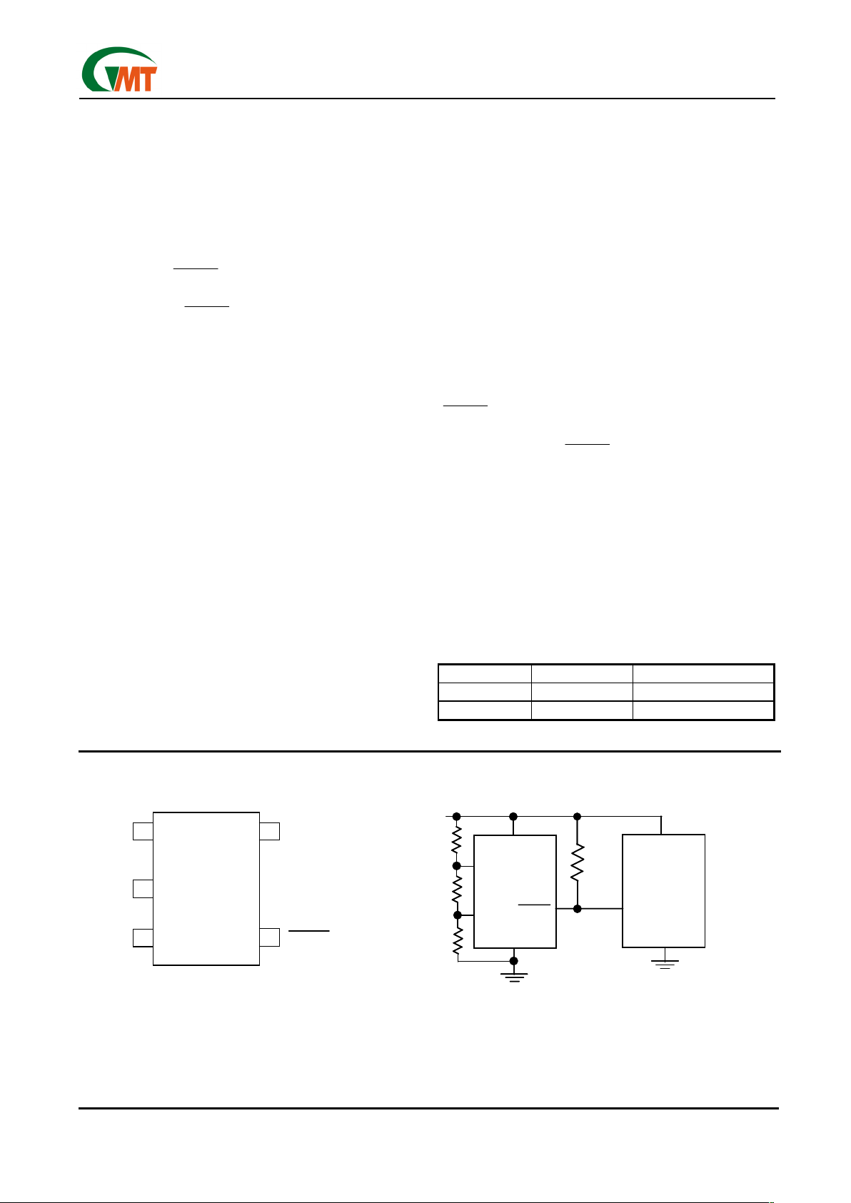
Pin Configuration Typical Operating Circuit
Vcc
RESET(RESET)
SOT23-5
5
4
1
HTH
2
3
GND
LTH
G680/G681
() is for G680H
RESET
INPUT
GND
µP
V
CC
RESET
(RESET)
GND
G680/G681
V
CC
R
PULL-UP
V
CC
*
*G681 ONLY
HTH
LTH
Vcc
RESET(RESET)
SOT23-5
5
4
1
HTH
2
3
GND
LTH
G680/G681
() is for G680H
Vcc
RESET(RESET)
SOT23-5
5
4
1
HTH
2
3
GND
LTH
G680/G681
() is for G680H
RESET
INPUT
GND
µP
V
CC
RESET
(RESET)
GND
G680/G681
V
CC
R
PULL-UP
V
CC
*
*G681 ONLY
HTH
LTH
Page 2
Ver: 1.1
Jun 07, 2002
TEL: 886-3-5788833
http://www.gmt.com.tw
2
G680/G681
Global Mixed-mode Technology Inc.
Absolute Maximum Ratings
Terminal Voltage (with respect to GND)
V
CC
.……………………………..……………-0.3V to +6.0V
Input Voltage (V
LTH
, V
HTH
)…..……….-0.3V to (VCC + 0.3V)
RESET,
RESET (push-pull)....…......-0.3V to (VCC + 0.3V)
RESET (open drain)...…........…........…....-0.3V to +6.0V
Input Current, V
CC
............................……................20mA
Output Current, RESET,
RESET ..….....................20mA
Continuous Power Dissipation (T
A
= +70°C)
SOT23-5…………………………………………….568mW
Operating Temperature Range …....….-40°C to +105°C
Storage Temperature Range..…...…….-65°C to +150°C
Lead Temperature (soldering, 10s) ...…....…......+300°C
Stresses beyond those listed under “Absolute Maximum Ratings” may cause permanent damage to the device. These are stress rat-
ings only, and functional operation of the device at these or any other conditions beyond those indicated in the operational sections of
the specifications is not implied. Exposure to absolute maximum rating conditions for extended periods may affect device reliability.
Electrical Characteristics
(VCC = full range, TA = -40°C to +105°C, unless otherwise noted. Typical values are at TA = +25°C, VCC = 3.3V (Note 1)
PARAMETER SYMBOL CONDITION MIN TYP MAX UNITS
VCC Range 2.5 5.5 V
Supply Current (SOT23)
I
CC
V
CC
<5.5V
4 7.5
µA
Reset Threshold VTH 1.23 1.25 1.29 V
Reset Threshold Tempco 70 ppm/°C
V
LTH
to Reset Delay (Note 2) V
LTH
= VTH to VTH – 100mV 15 µs
VCC = 2.5V 80 250 550
Reset Active Timeout Period
V
CC
= 5.5V 500
ms
RESET
(RESET) Output Current Low
I
OL
V
CC
= 2.5V, V
RESET
(V
RESET
) = 0.5V,
RESET
Asserted or RESET not asserted
8 mA
RESET
Output Current High
(push-pull G680)
I
OH
V
CC
= 2.5V, V
RESET
(V
RESET)
= 2V,
RESET
not asserted or RESET asserted.
2 mA
Note 1: Production testing done at TA = +25°C; limits over temperature guaranteed by design.
Note 2:
RESET output is for G680L/G681L; While RESET output is for G680H.
Selector Guide
PART / SUFFIX OUTPUT TYPE
TOP MARK
G680LT1
Push-pull
RESET
680Ax
G680HT1 Push-pull RESET 680Bx
G681LT1
Open-Drain
RESET
681Ax
Page 3
Ver: 1.1
Jun 07, 2002
TEL: 886-3-5788833
http://www.gmt.com.tw
3
G680/G681
Global Mixed-mode Technology Inc.
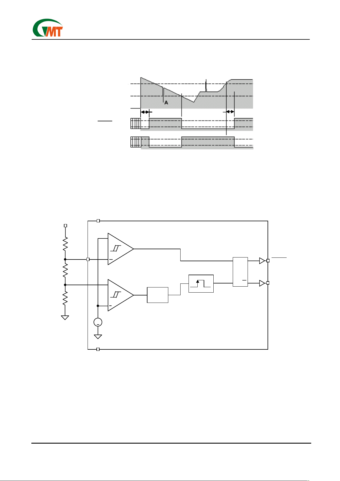
Timing Diagram
Functional Diagram
V
BATT
V
RESET
V
RESET
Propagation delays not shown for clarity.
V
HTH
V
LTH
0V
t
RST
t
RST
A
V
OH
V
OL
V
OH
V
OL
V
BATT
V
RESET
V
RESET
Propagation delays not shown for clarity.
V
HTH
V
LTH
0V
t
RST
t
RST
A
V
OH
V
OL
V
OH
V
OL
+
+
High-Voltage Detect
Delay
Line
RQ
SQ
One Shot
Low-Voltage Detect
+
1.24V
Bandgap
Reference
GND
G680/G681
RESET
RESET
V
DD
LTH
HTH
+
+
High-Voltage Detect
Delay
Line
RQ
SQ
One Shot
Low-Voltage Detect
+
1.24V
Bandgap
Reference
GND
G680/G681
RESET
RESET
V
DD
LTH
HTH
Page 4

Ver: 1.1
Jun 07, 2002
TEL: 886-3-5788833
http://www.gmt.com.tw
4
G680/G681
Global Mixed-mode Technology Inc.
Typical Operating Characteristics
(VCC = full range, TA = -40°C to +105°C, unless otherwise noted. Typical values are at TA = +25°C, VCC = 5V
for 463/438/400 versions, V
CC
= 3.3V for 308/293 versions, and VCC = 3V for 263 version.)
Power -Down Reset Delay
vs. Temperature
0
10
20
30
40
50
60
70
-40-20 0 20406080
Temperature(°C)
Power-Down Reset Delay(
μ
S)
VOD=10mV
V
OD=VTH-
VLTH
VOD=100mV
V
OD
=200mV
Supply Current vs.
Temperature
0
0.5
1
1.5
2
2.5
3
3.5
4
4.5
5
-40-200 20406080
Temperature (°C)
Supply Current (uA)
Vcc=5V
Vcc=3.3V
Vcc=2.5V
Normalized Reset Threshold
vs. Temperature
0.986
0.988
0.99
0.992
0.994
0.996
0.998
1
1.002
-40-30-20-100 10202730405060708090
Temperature (°C)
Normalized Reset Threshold (V)
Reset Timeout Period
vs. Temperature
0
100
200
300
400
500
600
700
800
-40-30-20-100 102030405060708090
Temperature (°C)
Reset Timeout Period (ms)
VCC=5.5V
V
CC
=3V
Page 5

Ver: 1.1
Jun 07, 2002
TEL: 886-3-5788833
http://www.gmt.com.tw
5
G680/G681
Global Mixed-mode Technology Inc.
Pin Description
PIN NAME FUNCTION
1 HTH
High-Voltage Theshold (Input): Analog input to a comparator. When the level on this pin initially
rises above V
TH
, the delay generator cycles and the
RESET
remains low or RESET remains high
for a minimum of 140ms.
2 GND Ground
3 LTH
Low-Voltage Threshold (Input): Analog input to a comparator. This is the voltage monitor input
assigned to detect a low voltage condition. When the level on this pin falls below V
TH
,
RESET
or
RESET is asserted and the condition is latched until V
HTH
> VTH.
4
RESET
(RESET)
Reset (Output): Push-pull output. This output is asserted and latched when V
LTH
<VTH, indicating
a low voltage condition. This state remains latched until V
HTH
> VTH. The polarity of this signal
(active-high or low) is determined by the part number suffix. See ordering information.
5 VCC Power Supply (Input): Independent supply input for internal circuitry.
Detailed Description
A microprocessor’s (µP’s) reset input starts the µP in a
known state. The G681L/G680L/G680H assert reset to
prevent code-execution errors during power-up,
power-down, or brownout conditions. They assert a
reset signal whenever the threshold voltage declines
below V
TH
, keeping it asserted for at least 140ms after
threshold voltage input has risen above the reset
threshold. The G681L uses an open-drain output, and
the G680L/G680H have a push-pull output stage.
Connect a pull-up resistor on the G681L’s
RESET out-
put to any supply between 0 and 5.5V.
Battery voltage is monitored by a comparator via a
voltage divider network. The divided voltage is compared to an internal reference voltage. When the voltage at the LTH input pin drops below the internal reference voltage, the output is asserted. At this point,
the voltage at HTH is assumed to be below the reference voltage.
Figure1. Maximum Transient Duration without
Causing a Reset Pulse vs. Reset Comparator Overdrive
Applications Information
Negative-Going VCC Transients
In addition to issuing a reset to the µP during
power-up, power-down, and brownout conditions, the
G681L/G680H/G680L are relatively immune to shortduration negative-going V
LTH
transients (glitches).
Figure1. shows typical transient duration vs. reset
comparator overdrive, for which the G681L/G680H/
G680L do not generate a reset pulse. The graph was
generated using a negative-going pulse applied to
V
LTH
, starting 0.1V above the actual reset threshold
and ending below it by the magnitude indicated (reset
comparator overdrive). The graph indicates the maximum pulse width a negative-going V
LTH
transient can
have without causing a reset pulse. As the magnitude
of the transient increases (goes farther below the reset
threshold), the maximum allowable pulse width decreases. Typically, a V
LTH
transient that goes 100mV
below the reset threshold and lasts 7µs or less will not
cause a reset pulse. A 0.1µF bypass capacitor
mounted as close as possible to the V
LTH
pin provides
additional transient immunity.
Programming the Thresholds
The low-voltage threshold is calculated using:
R1+R2+R3
V
BAT (Io)
= V
REF
R2+R3
The low-voltage threshold is calculated using:
R1+R2+R3
V
BAT (hi)
= V
REF
R3
where, for both equations:
V
BAT (hi)
= 1.245V
In order to provide the additional criteria needed to
solve for the resistor values, the resistors can be selected such that they have a given total value, that is,
R1 + R2 + R3 = R
TOTAL
.
0
50
100
150
200
250
300
350
1 10 100 1000
Reset Comparator Overdrive, VTH- V
LTH
(mV)
Maximum Transient Duration (us)
G680
Page 6

Ver: 1.1
Jun 07, 2002
TEL: 886-3-5788833
http://www.gmt.com.tw
6
G680/G681
Global Mixed-mode Technology Inc.
A value such as 1MΩ for R
TOTAL
is a reasonable value
because it draws minimum battery current but has no
measurable effect on accuracy.
When working with large resistors, a small amount of
leakage current can cause voltage offsets that
degrade system accuracy.
The maximum recommended total resistance from
V
BAT
to ground is 3MΩ.
Figure 2. Example Circuit
Once the desired trip points are determined, set the
V
BAT(hi)
threshold first.
For example, use a total of 1M = R1 + R2 + R3. For a
typical single-cell lithium ion battery, 3.6V is a good
“high threshold” because at 3.6V the battery is moderately charged. Solving for R3:
1MΩ
V
BAT (hi)
= 1.245
R3
R3 = 344kΩ
Once R3 is determined, the equation for V
BAT (lo)
can
be used to determine R2. A single lithium-ion cell
should not be discharged below 2.5V. Many applications limit the drain to 3.1V. Using 3.1V for the V
BAT (lo)
threshold allows calculation of the two remaining resistor values.
1MΩ
V
BAT (lo)
=3.1V = 1.245
R2+344k
R2 = 56kΩ
R1 = 1MΩ - R2 - R3
R 1=600kΩ
The accuracy of the resistors can be chosen based
upon the accuracy required by the system.
Figure 3. Interfacing to µPs with Bidirectional Re
set I/O
Interfacing to µPs with Bidirectional Reset Pins
Since the
RESET output on the G681L is open drain,
this device interfaces easily with µPs that have bidirectional reset pins, such as the Motorola 68HC11.
Connecting the µP supervisor’s
RESET output di-
rectly to the microcontroller’s (µC’s)
RESET pin with
a single pull-up resistor allows either device to assert
reset (Figure 3).
.
V
BATT
VCC
LTH
HTH
RESET
RESET
R1
R2
R3
604k
1%
56k
1%
340k
1%
G680/G681
V
BATT
VCC
LTH
HTH
RESET
RESET
R1
R2
R3
604k
1%
56k
1%
340k
1%
G680/G681
RESET
INPU T
GND
µP
V
CC
RESET
GND
G681
V
CC
V
CC
MOTOROLA
68HCXX
R
PULL-UP
RESET
INPU T
GND
µP
V
CC
RESET
GND
G681
V
CC
V
CC
MOTOROLA
68HCXX
R
PULL-UP
Page 7

Ver: 1.1
Jun 07, 2002
TEL: 886-3-5788833
http://www.gmt.com.tw
7
G680/G681
Global Mixed-mode Technology Inc.
Package Information
Note:
1. Package body sizes exclude mold flash protrusions or gate burrs
2. Tolerance ±0.1000 mm (4mil) unless otherwise specified
3. Coplanarity: 0.1000mm
4. Dimension L is measured in gage plane
DIMENSIONS IN MILLIMETERS
SYMBOLS
MIN NOM MAX
A 1.00 1.10 1.30
A1 0.00 ----- 0.10
A2 0.70 0.80 0.90
b 0.35 0.40 0.50
C 0.10 0.15 0.25
D 2.70 2.90 3.10
E 1.40 1.60 1.80
e ----- 1.90(TYP) -----
e1 ----- 0.95 -----
H 2.60 2.80 3.00
L 0.37 ------ -----
θ
1
1º 5º 9º
Taping Specification
GMT Inc. d oes not assume any responsibility for use of any circuitry described, no circuit patent licenses are implied and GMT Inc. reserves the right at any time without notice to change said circuitry and specifications.
E
e
D
H
θ
1
L
C
b
A2
A1
A
e1
E
e
D
H
θ
1
L
C
b
A2
A1
A
e1
Feed Direction
SOT23-5 Package Orientation
Feed Direction
SOT23-5 Package Orientation
 Loading...