

Page 1
Global Mixed-mode Technology Inc.
G525A
USB High-Side Power Switch Advance Information
Features
Typical 110m
5.0V
1A minimum continuous load current
3.0V to 5.5V operating range
100 µA typical on-state supply current
1 µA typical standby supply current
Output can be forced higher than input when
operating in off state.
1.4A Typical current limit
Thermal shutdown protection
2.4V typical under-voltage lockout (UVLO)
Open-drain fault flag pin
Slow turn-on (soft-start) and fast turnoff
Logic level enable pin, available with active-
high or active-low version
UL Approved_#E232223
, Low MOSFET on resistance, at
ΩΩΩΩ
Applications
High-side power protection switch
USB power management
USB host and self-powered hubs
USB Bus-powered hubs
Hot plug-in power supplies
Battery-charger circuits
General Description
The G525A is an integrated high-side power switch
optimized for self-powered and bus-powered Universal
Serial Bus (USB) applications.
The G525A satisfies the USB standards. The switch's
low on-resistance meets USB voltage drop requirements. When the output load exceeds current-limit
threshold, G525A switches into constant mode and
limit the output current to a safe level, which is typically
1.4A, well below the UL 25VA safety requirements. An
open-drain flag output is also available to indicate fault
conditions to the local USB controller. Soft start eliminates the momentary voltage drop on the upstream port
that may occur when the switch is enabled in
bus-powered applications.
Besides, a thermal shutdown circuit is included to prevent catastrophic switch failure caused by increasing
power dissipation when continuous heavy loads or
short circuit occurs. A under-voltage lockout (UVLO)
circuit ensures that the device remains off unless there
is a valid input voltage present, and an enable input
that is compatible with both 3.3V and 5V logic.
The G525A is a UL recognized component and is
available in active-high and active-low versions in 8-pin
SOP packages.
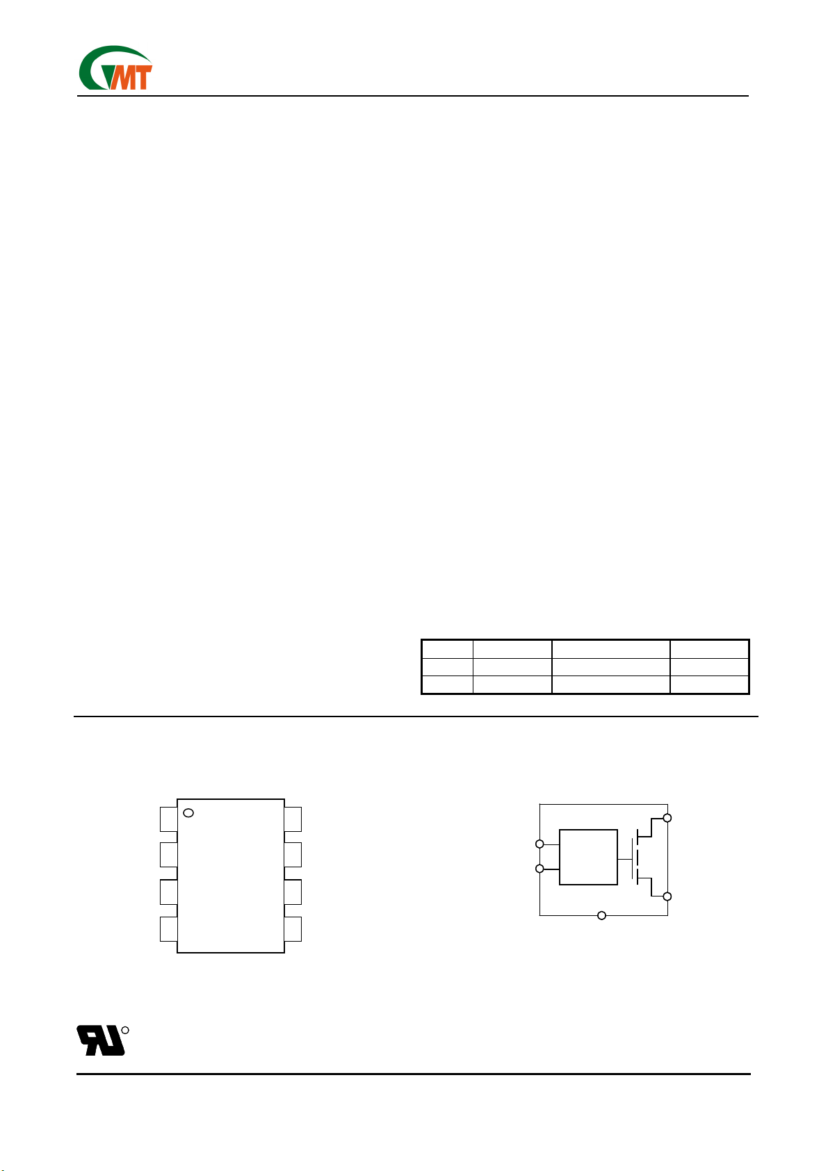
Pin Configuration
G525A
G525A
1
1
EN
EN
2
2
FLG
FLG
3
3
GND
GND
NC
NC
4
4
8 Pin SOP
8 Pin SOP
Ordering Information
PART ENABLE TEMP. RANGE PACKAGE
G525A1 Active High
G525A2 Active Low
8
8
OUT
OUT
(EN)1
IN
IN
7
7
6
6
OUT
OUT
5
5
NC
NC
(EN)1
(FLG)2
(FLG)2
-40°C to +85°C
-40°C to +85°C
G525A
G525A
Gate
Gate
Control
Control
3 (GND)
3 (GND)
8 Pin Function Block
8 Pin Function Block
8-Pin SOP
8-Pin SOP
6,8 (OUT)
6,8 (OUT)
7 (IN)
7 (IN)
R
R
UL Recognized Component
UL Recognized Component
Ver: 1.2
Nov 11, 2002
1
TEL: 886-3-5788833
http://www.gmt.com.tw
Page 2
Global Mixed-mode Technology Inc.
G525A
Absolute Maximum Ratings
Supply Voltage (VIN)..…………….….………...…..+6.0V
Fault Flag Voltage (V
Fault Flag Current (I
Output Voltage (V
Output Current (I
Enable Input (V
EN
Storage Temperature (T
)..…………..……...……..+6.0V
FLG
)……………………………50mA
FLG
)..…………………………….+6.0V
OUT
).………………….Internally Limited
OUT
)……………………………-0.3V to 6V
)….………....-65°C to +150°C
S
Operating Ratings
Supply Voltage (VIN).……………………….+3V to +5.5V
Operating Temperature (T
Thermal Resistance
SOIC (
)……………………………………160°C/W
θ
JA
)…………….-40°C to +85°C
A
Lead Temperature (Soldering 5 sec.)……………260°C
ESD protection*………………..…………….……….2kV
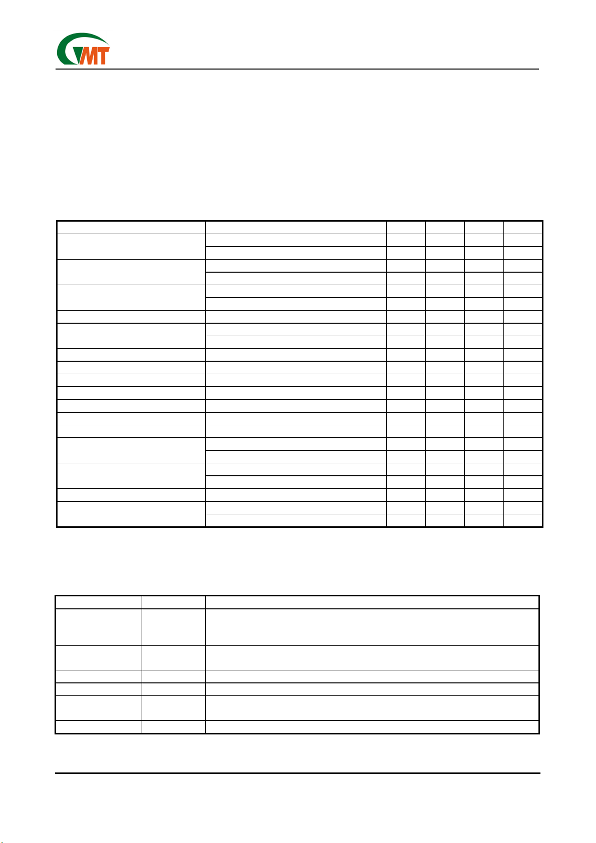
Electrical Characteristics
(VIN=+5V; TA=25°C.)
PARAMETER CONDITION MIN TYP MAX UNITS
switch off, OUT = open 1 5 µA
IN Supply Current
EN Enable Threshold
EN Input Current
EN Input Capacitance 1 pF
Switch Resistance
OUT Turn-On Delay RL = 10Ω 0.03 ms
OUT Turn-On Rise Time RL = 10Ω, CL=100µF 0.5 ms
OUT Turn-Off Delay RL = 10Ω 1 20 µs
OUT Turn-Off Fall Time RL = 10Ω 1 20 µs
OUT Leakage Current 1 10 µA
Short Circuit Current Limit Enable into load 1.0 1.4 2.0 A
Circuit Limit Threshold Ramped load applied to enabled output 2.0 2.7 3.5 A
Threshold
FLG Output Resistance
FLG Off Current V
UVLO Threshold
Devices are ESD protected, however, handling precautions are recommended.
*
For the G525A1, off is ≤ 1.0 and on is ≥2.5V. For the G525A2, off is ≥ 2.5V and on is ≤ 1.0V. The enable input,
**
**
switch on, OUT = open 100 160 µA
**
low to high transition 2.5 V
high to low transition ** 0.8 V
V
= V
EN
V
= V
EN
VIN = 5V , I
V
= 3.3V , I
IN
TJ increasing 135 °C Overtemperature Shutdown
T
decreasing 125 °C
J
VIN = 5V, IL=10mA 10 25
V
= 3.3V, IL =10mA 15 40
IN
FLAG
V
= increasing 2.5 V
IN
V
= decreasing 2.3 V
IN
= 2.5V 0.01 1 µA
OH(min)
= 1.0V 0.01 1 µA
OL(max)
= 500mA 110 140 mΩ
OUT
= 500mA 130 180 mΩ
OUT
Ω
Ω
= 5V 0.01 1 µA
CTRL, has approximately 200mV of hysteresis.
Pin Description
PIN NUMBER PIN NAME PIN FUNCTION
: Logic level enable input. High input >2.4V typical.
: Active-low, open-drain output. Indicates overcurrent,
.
: Output MOSFET source, which also supplies IC's internal circuitry. Con-
: Output MOSFET drain. Typically connect to switched side of load.
2
1 EN
2 FLG
3 GND
4,5 NC Not internally connected.
7 IN
6,8 OUT
Ver: 1.2
Nov 11, 2002
Enable (input)
Low input <2.2V typical (1 for active high, 2 for active low).
Make sure EN never floating.
Open-Drain Fault Flag (Output)
thermal shutdown and UVLO.
Ground
Input Supply
nect to positive supply.
Switch Output
TEL: 886-3-5788833
http://www.gmt.com.tw
Page 3
Global Mixed-mode Technology Inc.
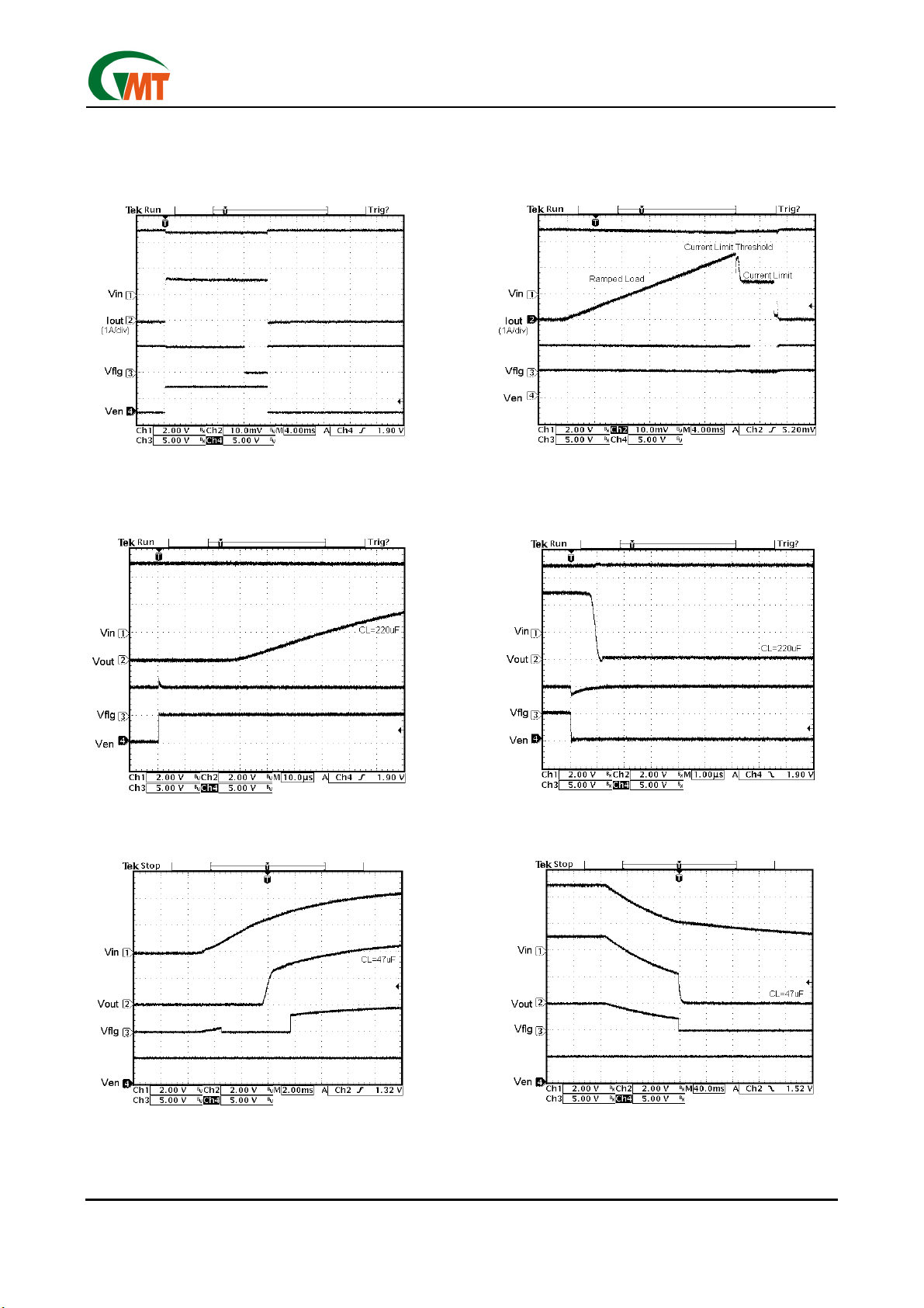
TYPICAL PERFORMANCE CHARACTERISTICS
(VIN= 5V, TA=25
C, G525A1, unless otherwise noted.)
°°°°
G525A
Flag Delay After OC
Output Turn-On Delay
Iout Ramp Chart
Output Turn-Off Delay
Ver: 1.2
Nov 11, 2002
Power Up (UVLO)
3
Power Down (UVLO)
TEL: 886-3-5788833
http://www.gmt.com.tw
Page 4

Global Mixed-mode Technology Inc.
TYPICAL PERFORMANCE CHARACTERISTICS
(VIN= 5V,TA=25
C, G525A1, unless otherwise noted.)
°°°°
G525A
Turn-On Characteristics
Turn-On Characteristics
Turn-On Characteristics
Turn-On Characteristics
Short Circuit Response
(Short Applied to Output)
Ver: 1.2
Nov 11, 2002
4
TEL: 886-3-5788833
http://www.gmt.com.tw
Page 5

Global Mixed-mode Technology Inc.
Typical Applications
Upstream
Upstream
V
V
BUS
BUS
100mA max.
100mA max.
V
V
BUS
BUS
D
D
+
+
D
D
-
-
GND
GND
1µF
1µF
Data
Data
IN
IN
G912
G912
OUT
OUT
GND
GND
10k
10k
3.3V USB Controller
3.3V USB Controller
VIN
VIN
OVERCURRENT
OVERCURRENT
1 µF
1 µF
GND
GND
ON/OFF
ON/OFF
100k
100k
G525A
G525A
EN
EN
FLG
FLG
GND
GND
NC
NC
OUT
OUT
IN
IN
OUT
OUT
NC
NC
V
V
CC
CC
5.0V
5.0V
150 µF
150 µF
0.1 µF
0.1 µF
Ferrite
Ferrite
Beads
Beads
+
+
Data
Data
G525A
V
V
BUS
BUS
D
D
+
+
USB
USB
D
D
-
-
Port
Port
GND
GND
Single-Port Self-Powered USB Hub Application
Function Block Diagrams
EN
EN
Clock
Clock
BandGap
BandGap
Reference
Reference
UVLO
UVLO
GND
GND
Thermal Sense
Thermal Sense
IN
IN
Gate Control
Gate Control
Overcurrent
Overcurrent
Limiting
Limiting
CMP
CMP
Current
Current
Sense
Sense
OUT
OUT
FLG
FLG
Functional Description
The G525A1 and G525A2 are high-side 1-channel
switches with active-high and active-low enable inputs,
respectively. Fault conditions turn off or inhibit turn-on
of the output transistors and activate the open-drain
error flag transistors to pull FLG pin to ground.
Input and Output
IN (input) is the power supply connection to the logic
circuitry and the source of the output MOSFET. OUT
(output) is the drain of the output MOSFET. In a typical
application, current flows through the switch from IN to
OUT toward the load. Both OUT pins must be
connected together to the load.
Ver: 1.2
Nov 11, 2002
The output MOSFET and driving circuit are also designed to allow the MOSFET drain to be externally
forced to a higher voltage than the source (V
OUT
when the switch is off. In this situation, the G525A
avoids undesirable drain-to-body diode current flow by
connecting the body to the most positive voltage. If
V
OUT >VIN
from V
when switch is enabled, current will flow
to VIN.
OUT
Thermal Shutdown
Thermal shutdown protects G525A from excessive
power dissipation. If the die temperature exceeds
135°C, the MOSFETS switch is shut off and a fault
flag is activated. 10°C of hystersis prevents the switch
TEL: 886-3-5788833
http://www.gmt.com.tw
5
> VIN)
Page 6

from turning on until the die temperature drops to
125°C. Thermal shutdown circuit functions only when
the switch is enabled.
Undervoltage Lockout
UVLO (undervoltage lockout) prevents the output
MOSFET from turning on until IN (input voltage) exceeds 2.5V typically. After the switch turns on, if the
voltage drops below 2.3V typically, UVLO shuts off the
output MOSFET and signals the fault flag. UVLO detection functions only when the switch is enabled.
Current Sensing and Limiting
The current limit threshold is preset internally. The
preset level prevents damage to the output MOSFET
and external load but allows a minimum current of
0.5A through the output MOSFET.
A current sense circuit senses the output current of
MOSFET switch. If output current exceeds the current
limit threshold, the output MOSFET switch is shut off
and a fault flag is pulled low. The reaction to an overcurrent is measured with the following scenarios:
Switch Enabled into Heavy Load
If the switch is powered on or enabled into a heavy
load or short-circuit, the switch immediately goes into
a constant-current mode, reducing the output voltage.
The fault flag goes low until the load is reduced or
thermal shutdown occurs. See the "Enable into Short
Circuit" graph.
Global Mixed-mode Technology Inc.
G525A
Fault Flag
FLG is a 2-channel, open-drain MOSFET output. The
fault-flag is active (low) for one or more of the following conditions: current limiting, undervoltage, or thermal shutdown. The flag output MOSFET is capable of
sinking a 10mA load to typically 100mV above ground.
Applications Information
Supply filtering
A 0.1µF to 1µF bypass capacitor from IN to GND, located near the G525A, is strongly recommended to
control supply transients. Without a bypass capacitor,
an output short may cause sufficient ringing on the
input (from supply lead inductance) to damage internal
control circuitry.
Input transients must not exceed the absolute maximum supply voltage (V
ration.
Figure 1. Supply Bypassing
G525A
G525A
EN
EN
1
1
= 6V) even for a short du-
IN max
3.0V to 5.5V
3.0V to 5.5V
8
8
OUT
OUT
Heavy Load Applied to Enabled Switch
When a heavy load is applied, a large current may
flow from the switch. The current limit circuit may shut
the switch off briefly, then fold back into constant-current mode. In that case, the fault flag falls
until the load is reduced. See the “Short Applied to
Output” graph and the "Ramped Load to Enable Device" graph.
G525A
G525A
V
V
BUS
BUS
USB Host
USB Host
GND
GND
Cable
Cable
4.7
4.7
µF
µF
1
1
EN
EN
2
2
FLG
FLG
3
3
GND
GND
NC
NC
4
4
Bus Powered Hub
Bus Powered Hub
OUT
OUT
IN
IN
OUT
OUT
NC
NC
0.1 µF
0.1 µF
8
8
7
7
6
6
5
5
USB
USB
Controller
Controller
7
2
2
FLG
FLG
3
3
GND
GND
4
4
NC
NC
C
C
BULK
BULK
Downstream USB Device
Cable
Cable
Downstream USB Device
IN
IN
OUT
OUT
NC
NC
7
6
6
5
5
Capacitive
Capacitive
Load
Load
0.1 µF to 1 µF
0.1 µF to 1 µF
Ver: 1.2
Nov 11, 2002
Figure 2. Soft Start
6
TEL: 886-3-5788833
http://www.gmt.com.tw
Page 7

EN, the enable Input
EN, with 0.2V hysteresis, must be driven logic high or
logic low for a clearly defined input. Floating the input
may cause unpredictable operation. EN should not be
allowed to go negative with respect to GND.
Soft Start
The G525A is high impedance when off and slowly
becomes a low impedance as it turns on. This reduces
inrush current and related voltage drop that results
from charging a capacitive load, satisfying the USB
voltage drop requirements, for bus-powered applications as shown in Figure 2.
The soft start circuit shown in Figure 3 can be utilized
to meet USB transient regulation specifications with
large load capacitances (C
will provide inrush current limiting for these applications.
Global Mixed-mode Technology Inc.
18
18
EN
V
V
BUS
BUS
USB Hub
USB Hub
GND
GND
Cable
Cable
Figure 3. Inrush Current-Limit Application
>10µF). The G525A
BULK
4.7
4.7
µF
µF
EN
2
2
FLG
FLG
3
3
GND
GND
NC
NC
4
4
USB Peripheral
USB Peripheral
G525A
G525A
OUT
OUT
OUT
OUT
IN
IN
NC
NC
USB
USB
USB
Controller
Controller
Controller
7
7
USB
USB
C
C
BULK
BULK
USB
Function
Function
Function
6
6
5
5
G525A
Transient Overcurrent Filter
V
V
+
+
10k
OVERCURRENT
OVERCURRENT
To USB
To USB
10k
10k
10k
0.1 µF
0.1 µF
1
1
2
2
3
3
4
4
G525A
G525A
EN
EN
FLG
FLG
GND
GND
NC
NC
OUT
OUT
OUT
OUT
NC
NC
8
8
IN
IN
7
7
6
6
5
5
Figure 4. Transient Filter
The inrush current from the connection of a heavy capacitive load may cause the fault flag to fall for a short
duration while the switch is in a constant-current mode,
for charging the capacitance. If needed, a simple 1ms
RC low-pass filter in series with the fault flag circuit
will prevent erroneous overcurrent reporting (see Figure 4).
Ver: 1.2
Nov 11, 2002
TEL: 886-3-5788833
http://www.gmt.com.tw
7
Page 8

Global Mixed-mode Technology Inc.
Package Information
7 °(4X)
E
H
D
A2
A
G525A
C
L
θ
y
Note:
1. Package body sizes exclude mold flash and gate burrs
2. Dimension L is measured in gage plane
3. Tolerance 0.10mm unless otherwise specified
4. Controlling dimension is millimeter converted inch dimensions are not necessarily exact.
SYMBOL
A 1.35 1.60 1.75 0.053 0.063 0.069
A1 0.10 ----- 0.25 0.004 ----- 0.010
A2 ----- 1.45 ----- ----- 0.057 -----
B 0.33 ----- 0.51 0.013 ----- 0.020
C 0.19 ----- 0.25 0.007 ----- 0.010
D 4.80 ----- 5.00 0.189 ----- 0.197
E 3.80 ----- 4.00 0.150 ----- 0.157
e ----- 1.27 ----- ----- 0.050 -----
H 5.80 ----- 6.20 0.228 ----- 0.244
L 0.40 ----- 1.27 0.016 ----- 0.050
y ----- ----- 0.10 ----- ----- 0.004
θ
MIN. NOM. MAX. MIN. NOM. MAX.
0º ----- 8º 0º ----- 8º
DIMENSION IN MM DIMENSION IN INCH
e
B
A1
Taping Specification
Feed Direction
Feed Direction
Typical SOP Package Orientation
Typical SOP Package Orientation
GMT Inc. d oes not assume any responsibility for use of any circuitry described, no circuit patent licenses are implied and GMT Inc. reserves the right at any ti me without notice to change said circuitry and specifications.
Ver: 1.2
Nov 11, 2002
8
TEL: 886-3-5788833
http://www.gmt.com.tw
 Loading...