

Datasheet G5250A1T1U, G5250A1TOU, G5250A2T1U, G5250A2TOU, G5250B1T1U Datasheet (GMT) [ru]
...Page 1
G5
250
Global Mixed-mode Technology Inc.
Power Distribution Switch
Features
85mΩΩΩΩ High-Side MOSFET
Available with 4 Versions of Current Limits with
Foldback
Operating Range:2.7V to 5.5V
400µS Typical Rise Time
Under Voltage Lockout
65µA Quiescent Supply Current
1µA Maximum Shutdown Supply Current
Logic Level Enable Pin, Available with
Active-High or Active-Low Version
No Reverse Current when Power Off
Deglitched Open-Drain Over-Current Flag
Output (OC)
Available for 3 Kinds of Pin Out (G5250 E/F/G/H)
(G5250 I/J/K/L) (G5250M/N/P)
Output Shutdown Pull-Low Resistor (G5250
I/J/K/L/M/N)
SOT-23-5 and TSOT-23-5 Package
UL Approved_#E232223
Nemko IEC 60950-1 CB/CCA_scheme certification Report #67291
CSA Approved #230321
Applications
High-Side Power Protection Switch
USB Power Management
USB Host and Self-Powered Bubs
USB Bus-Powered Hubs
Hot Plug-In Power Supplies
Battery-Charger Circuits
General Description
The G5250 is an integrated 85mΩ power switch for
self-powered and bus-powered Universal Serial Bus
(USB) applications.
Several Protection features include current limiting
with foldback, and thermal shutdown to prevent catastrophic switch failure caused by increasing power dissipation when continuous heavy loads or short circuit
occurs. And a built-in charge pump is used to drive the
N-channel MOSFET that is free of parasitic body diode to eliminate any reversed current flow across the
switch when it is powered off.
G5250E/F/G/H, G5250I/J/K/L and G5250M/N/P has
open- drain
over-temperature event and has typical 9ms deglitch
timeout period.
OC
output reports over-current or
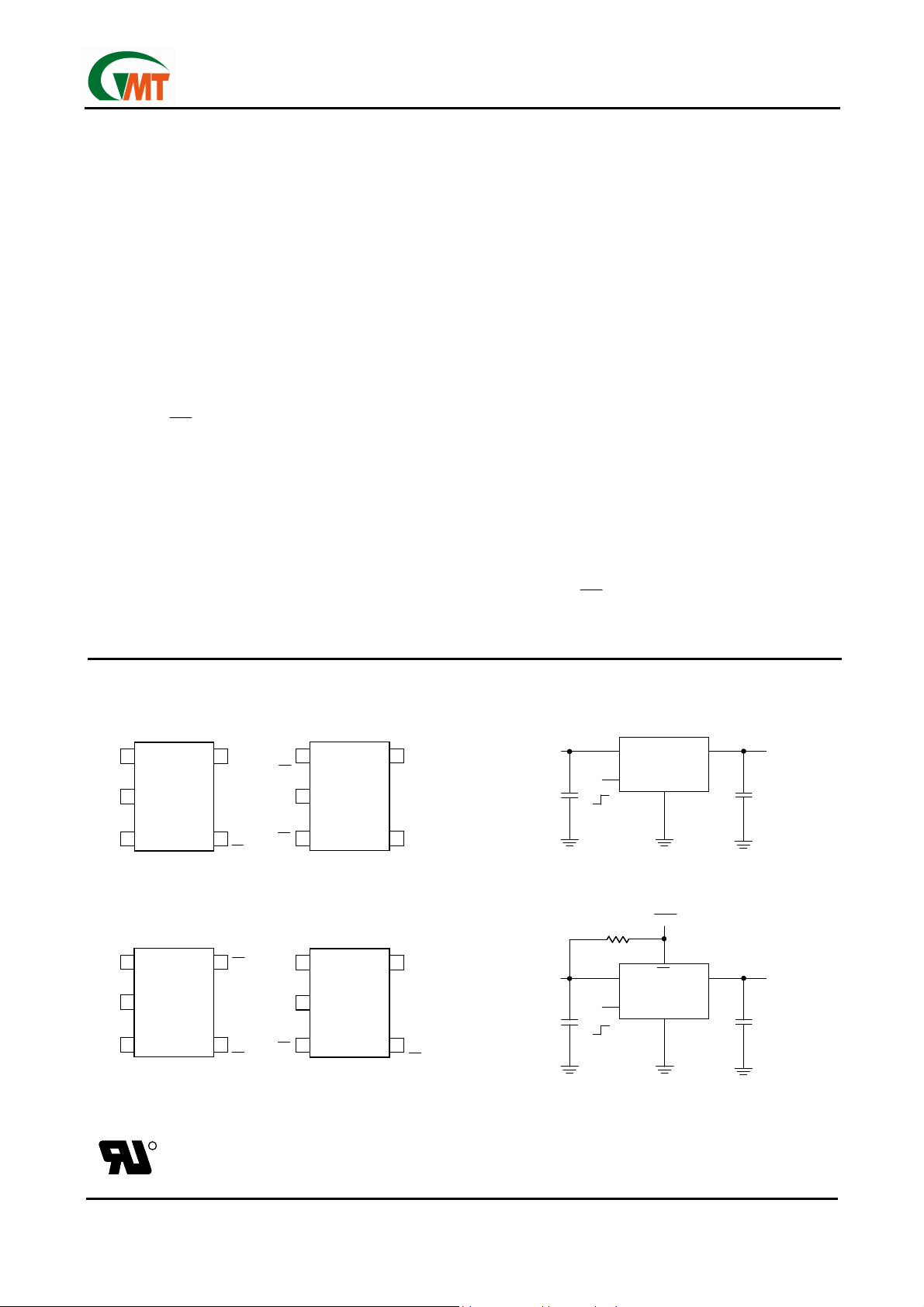
Pin Configuration Typical Application Circuit
G5250A/B/C/D
OFF
OFF
ON
ON
G5250A/B/C/D
IN
IN
EN
EN
GND
GND
OUT
OUT
OUT
OUT
GND
GND
IN23
IN23
G5250A/B/C/D
G5250A/B/C/D
1
1
SOT-23-5/TSOT-23-5
SOT-23-5/TSOT-23-5
G5250I/J/K/L
G5250I/J/K/L
V
V
IN
C
C
1µF
1µF
IN
IN
IN
OUT
EN 5
1
EN 5
5
5
OUT
OUT
EN
EN
4
4
(EN)
(EN)
1
(EN)
(EN)
2
2
GND
GND
OC
OC
3
3
SOT-23-5/TSOT-23-5
SOT-23-5/TSOT-23-5
OUT
IN
IN
4
4
G5250E/F/G/H,G5250I/J/K/L,G5250M/N/P
OUT
OUT
G5250E/F/G/H
G5250E/F/G/H
1
1
5
5
OC
OC
OUT
OUT
2
2
GND
GND
GND
GND
IN
IN
3
3
SOT-23-5/TSOT-23-5 SOT-23-5/TSOT-23-5
SOT-23-5/TSOT-23-5 SOT-23-5/TSOT-23-5
EN
EN
4
4
(EN)
(EN)
OC
OC
G5250M/N/P
G5250M/N/P
1
1
2
2
3
3
IN
IN
5
5
EN
EN
4
4
(EN)
(EN)
G5250E/F/G/H,G5250I/J/K/L,G5250M/N/P
FLAG
FLAG
OC
OC
IN
IN
EN
EN
GND
GND
OUT
OUT
V
V
C
C
1µF
1µF
100kΩ
100kΩ
IN
IN
ON
ON
IN
IN
OFF
OFF
R
R
C
C
OUT
OUT
22µF
22µF
C
C
OUT
OUT
22µF
22µF
V
V
OUT
OUT
V
V
OUT
OUT
UL Recognized Component
UL Recognized Component
Ver: 2.1
Aug 01, 2011
1
TEL: 886-3-5788833
http://www.gmt.com.tw
Page 2

G5
250
Global Mixed-mode Technology Inc.
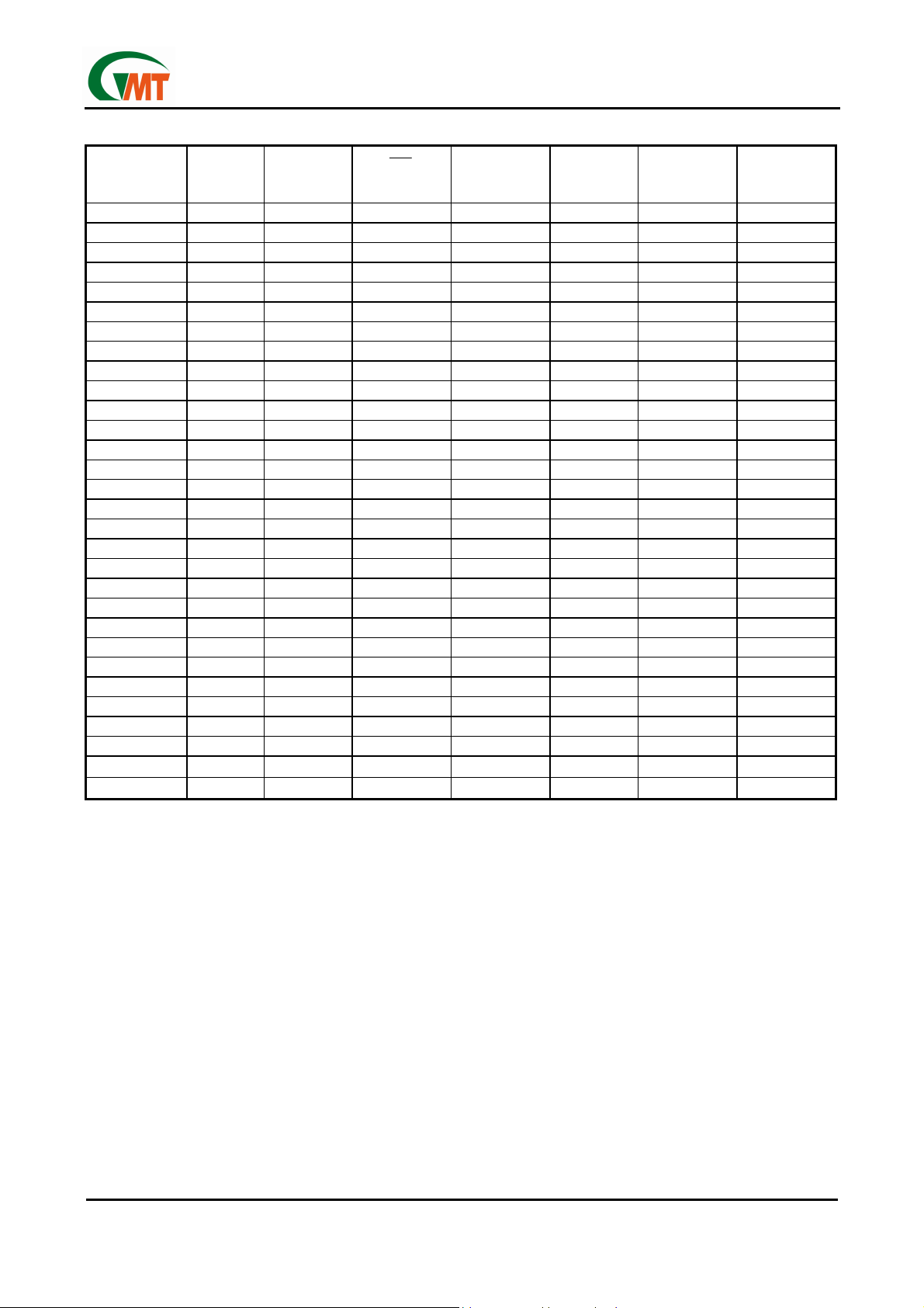
Ordering Information
ORDER
NUMBER
G5250A1T1U 50A1x Active High
G5250A2T1U 50A2x Active Low
G5250B1T1U 50B1x Active High
G5250B2T1U 50B2x Active Low
G5250C1T1U 50C1x Active High
G5250C2T1U 50C2x Active Low
G5250D1T1U 50D1x Active High
G5250D2T1U 50D2x Active Low
G5250E1T1U 50E1x Active High
G5250E2T1U 50E2x Active Low
G5250F1T1U
G5250F2T1U
G5250G1T1U 50G1x Active High
G5250G2T1U 50G2x Active Low
G5250H1T1U 50H1x Active High
G5250H2T1U 50H2x Active Low
G5250I1T1U
G5250I2T1U
G5250J1T1U
G5250J2T1U
G5250K1T1U 50K1x Active High
G5250K2T1U 50K2x Active Low
G5250L1T1U
G5250L2T1U
G5250M1T1U 50M1x Active High
G5250M2T1U 50M2x Active Low
G5250N1T1U 50N1x Active High
G5250N2T1U 50N2x Active Low
G5250P1T1U 50P1x Active High
G5250P2T1U 50P2x Active Low
Note: T1: SOT-23-5
U: Tape & Reel
MARKING ENABLE
50F1x Active High
50F2x Active Low
50I1x Active High
50I2x Active Low
50J1x Active High
50J2x Active Low
50L1x Active High
50L2x Active Low
OC
OUTPUT
No No 2.5A -40°C to +85°C SOT-23-5
No No 2.5A -40°C to +85°C SOT-23-5
No No 2.0A -40°C to +85°C SOT-23-5
No No 2.0A -40°C to +85°C SOT-23-5
No No 1.5A -40°C to +85°C SOT-23-5
No No 1.5A -40°C to +85°C SOT-23-5
No No 1.0A -40°C to +85°C SOT-23-5
No No 1.0A -40°C to +85°C SOT-23-5
Yes No 2.5A -40°C to +85°C SOT-23-5
Yes No 2.5A -40°C to +85°C SOT-23-5
Yes No 2.0A -40°C to +85°C SOT-23-5
Yes No 2.0A -40°C to +85°C SOT-23-5
Yes No 1.5A -40°C to +85°C SOT-23-5
Yes No 1.5A -40°C to +85°C SOT-23-5
Yes No 1.0A -40°C to +85°C SOT-23-5
Yes No 1.0A -40°C to +85°C SOT-23-5
Yes Yes 2.5A -40°C to +85°C SOT-23-5
Yes Yes 2.5A -40°C to +85°C SOT-23-5
Yes Yes 2.0A -40°C to +85°C SOT-23-5
Yes Yes 2.0A -40°C to +85°C SOT-23-5
Yes Yes 1.5A -40°C to +85°C SOT-23-5
Yes Yes 1.5A -40°C to +85°C SOT-23-5
Yes Yes 1.0A -40°C to +85°C SOT-23-5
Yes Yes 1.0A -40°C to +85°C SOT-23-5
Yes Yes 1.0A -40°C to +85°C SOT-23-5
Yes Yes 1.0A -40°C to +85°C SOT-23-5
Yes Yes 1.5A -40°C to +85°C SOT-23-5
Yes Yes 1.5A -40°C to +85°C SOT-23-5
Yes Yes 2A -40°C to +85°C SOT-23-5
Yes Yes 2A -40°C to +85°C SOT-23-5
OUTPUT
SHUTDOWN
DISCHARGE
CURRENT
LIMIT
TEMP.
RANGE
PACKAGE
(Green)
Ver: 2.1
Aug 01, 2011
2
TEL: 886-3-5788833
http://www.gmt.com.tw
Page 3
G5
250
Global Mixed-mode Technology Inc.
Ordering Information
ORDER
NUMBER
G5250A1TOU 50A1x Active High
G5250A2TOU 50A2x Active Low
G5250B1TOU 50B1x Active High
G5250B2TOU 50B2x Active Low
G5250C1TOU 50C1x Active High
G5250C2TOU 50C2x Active Low
G5250D1TOU 50D1x Active High
G5250D2TOU 50D2x Active Low
G5250E1TOU 50E1x Active High
G5250E2TOU 50E2x Active Low
G5250F1TOU 50F1x Active High
G5250F2TOU 50F2x Active Low
G5250G1TOU 50G1x Active High
G5250G2TOU 50G2x Active Low
G5250H1TOU 50H1x Active High
G5250H2TOU 50H2x Active Low
G5250I1TOU
G5250I2TOU
G5250J1TOU 50J1x Active High
G5250J2TOU 50J2x Active Low
G5250K1TOU 50K1x Active High
G5250K2TOU 50K2x Active Low
G5250L1TOU 50L1x Active High
G5250L2TOU 50L2x Active Low
G5250M1TOU 50M1x Active High
G5250M2TOU 50M2x Active Low
G5250N1TOU 50N1x Active High
G5250N2TOU 50N2x Active Low
G5250P1TOU 50P1x Active High
G5250P2TOU 50P2x Active Low
Note:TO: TSOT-23-5
U: Tape & Reel
MARKING ENABLE
50I1x Active High
50I2x Active Low
OC
OUTPUT
No No 2.5A -40°C to +85°C TSOT-23-5
No No 2.5A -40°C to +85°C TSOT-23-5
No No 2.0A -40°C to +85°C TSOT-23-5
No No 2.0A -40°C to +85°C TSOT-23-5
No No 1.5A -40°C to +85°C TSOT-23-5
No No 1.5A -40°C to +85°C TSOT-23-5
No No 1.0A -40°C to +85°C TSOT-23-5
No No 1.0A -40°C to +85°C TSOT-23-5
Yes No 2.5A -40°C to +85°C TSOT-23-5
Yes No 2.5A -40°C to +85°C TSOT-23-5
Yes No 2.0A -40°C to +85°C TSOT-23-5
Yes No 2.0A -40°C to +85°C TSOT-23-5
Yes No 1.5A -40°C to +85°C TSOT-23-5
Yes No 1.5A -40°C to +85°C TSOT-23-5
Yes No 1.0A -40°C to +85°C TSOT-23-5
Yes No 1.0A -40°C to +85°C TSOT-23-5
Yes Yes 2.5A -40°C to +85°C TSOT-23-5
Yes Yes 2.5A -40°C to +85°C TSOT-23-5
Yes Yes 2.0A -40°C to +85°C TSOT-23-5
Yes Yes 2.0A -40°C to +85°C TSOT-23-5
Yes Yes 1.5A -40°C to +85°C TSOT-23-5
Yes Yes 1.5A -40°C to +85°C TSOT-23-5
Yes Yes 1.0A -40°C to +85°C TSOT-23-5
Yes Yes 1.0A -40°C to +85°C TSOT-23-5
Yes Yes 1.0A -40°C to +85°C TSOT-23-5
Yes Yes 1.0A -40°C to +85°C TSOT-23-5
Yes Yes 1.5A -40°C to +85°C TSOT-23-5
Yes Yes 1.5A -40°C to +85°C TSOT-23-5
Yes Yes 2A -40°C to +85°C TSOT-23-5
Yes Yes 2A -40°C to +85°C TSOT-23-5
OUTPUT
SHUTDOWN
DISCHARGE
CURRENT
LIMIT
TEMP.
RANGE
PACKAGE
(Green)
Ver: 2.1
Aug 01, 2011
3
TEL: 886-3-5788833
http://www.gmt.com.tw
Page 4
G5
250
Absolute Maximum Ratings
Supply Voltage (VIN) . . . . . . . . . . . . . . . . . . . . . . . 6V
Output Voltage (V
Output Current (I
Enable Input (VEN) . . . . . . . . . . . . . . . . . . -0.3V to 6V
Thermal Resistance Junction to Ambient, (θJA)*
SOT-23-5/TSOT-23-5 . . . . . . . . . . . . . . . . . 250°C/W
Continuous Power Dissipation (TA=25°C)*
SOT-23-5/TSOT-23-5 . . . . . . . . . . . . . . . . . . . . . . 0.4W
Thermal Resistance Junction to Case, (θJc)
SOT-23-5/TSOT-23-5 . . . . . . . . . . . . . . . . . .60°C/W
* Please refer to Minimum Footprint PCB Layout Section.
Global Mixed-mode Technology Inc.
Storage Temperature (TS) . . . . . . . . .-65°C to +150°C
) . . . . . . . . . . . . . . . . . . . . . ..6V
OUT
) . . . . . . . . . . . .Internally Limited
OUT
Junction Temperature . . . . . . . . . . . . . . . . . . . . .150°C
Reflow Temperature (soldering, 10sec) . . . . . . . 260°C
ESD protection . . . . . . . . . . . . . . . . . . . . . . . . . . . . 2kV
Operating Ratings
Supply Voltage (VIN) . . . . . . . . . . . . . . . . .+3V to +5.5V
Operating Temperature (TA). . . . . . . . .-40°C to +85°C
Electrical Characteristics
VIN = 5V, CIN=1µF, C
PARAMETER CONDITION MIN TYP MAX UNITS
Input Voltage Rage
Output MOS R
Supply Current --- 65 95 µA
Output Turn-on Rising Time RL=10Ω, 90% Settling --- 400
Output Turn-off Falling Time RL=5Ω, C
Current Limit Threshold
Short-circuit Current
EN Input Threshold 1.4 1.6 1.8 V
Shutdown Supply Current --- 0.1 1 µA
Shutdown Pull-low Resistance G5250 I/J/K/L/M/N only --- 75 150
Output Leakage Current EN=”0”, V
VIN Under Voltage Lockout 2.2 2.5 2.7 V
VIN Under Voltage Hysteresis
Thermal Limit --- 135
Thermal Limit Hysteresis --- 20 --- °C
OCDeglitch G5250E/F/G/H/I/J/K/L/M/N/P,OC assertion or deassertion
OCOutput Low Voltage
OCOff-State Current
DS(ON)
=1µF, RL=10ΩΩΩΩ TA = 25°C, unless otherwise noted.
OUT
G5250A1/G5250A2/G5250E1/G5250E2/G5250I1/G5250I2,
I
=2A
OUT
G5250B1/G5250B2/G5250F1/G5250F2/G5250J1/G5250J2/
G5250P1/G5250P2, I
G5250C1/G5250C2/G5250G1/G5250G2/G5250K1/G5250K2,
G5250N1/G5250N2, I
G5250D1/G5250D2/G5250H1/G5250H2/G5250L1/G5250L2/
G5250M1/G5250M2, I
=1µF, 90% Settling --- 1.8 ---
OUT
G5250A1/G5250A2/G5250E1/G5250E2/G5250I1/G5250I2,
V
=4V, 2.7V<VIN<5.5V
OUT
G5250B1/G5250B2/G5250F1/G5250F2/G5250J1/G5250J2/
G5250P1/G5250P2, V
G5250C1/G5250C2/G5250G1/G5250G2/G5250K1/G5250K2/
G5250N1/G5250N2, V
G5250D1/G5250D2/G5250H1/G5250H2/G5250L1/G5250L2/
G5250M1/G5250M2, V
G5250A1/G5250A2/G5250E1/G5250E2/G5250I1/G5250I2,
V
=0V, 2.7V<VIN<5.5V
OUT
G5250B1/G5250B2/G5250F1/G5250F2/G5250J1/G5250J2/
G5250P1/G5250P2, V
G5250C1/G5250C2/G5250G1/G5250G2/G5250K1/G5250K2/
G5250N1/G5250N2, V
G5250D1/G5250D2/G5250H1/G5250H2/G5250L1/G5250L2/
G5250M1/G5250M2, V
=0V --- 0.5 1 µA
OUT
--- 200
G5250E/F/G/H/I/J/K/L/M/N/P, IOC= 5mA
G5250E/F/G/H/I/J/K/L/M/N/P, VOC= 5V
=1.5A
OUT
=1A
OUT
=0.5A
OUT
=4V, 2.7V<VIN<5.5V
OUT
=4V, 2.7V<VIN<5.5V
OUT
=4V, 2.7V<VIN<5.5V
OUT
=0V, 2.7V<VIN<5.5V
OUT
=0V, 2.7V<VIN<5.5V
OUT
=0V, 2.7V<VIN<5.5V
OUT
2.7 --- 5.5 V
--- 85 95 mΩ
--- µs
2 2.5 3.5
1.5 2 2.8
1.1 1.5 2.1
0.7 1 1.4
0.2 1.6 2.3
0.2 1.3 1.9
0.2 1 1.4
0.2 0.67
4 9 15 ms
--- --- 0.4 V
--- --- 1
1
--- mV
--- °C
ms
A
A
Ω
µ
A
Ver: 2.1
Aug 01, 2011
4
TEL: 886-3-5788833
http://www.gmt.com.tw
Page 5
G5
250
Global Mixed-mode Technology Inc.
Typical Performance Characteristics
(VIN= 5V, G5250B1, CIN=1µF, C
Turn on Delay Time and Rise Time Turn off Delay Time and Fall Time
=1µF, VEN=VIN, TA=25°C, unless otherwise noted.)
OUT
Inrush Current With Different Load Capacitance Thermal Shutdown Response
UVLO Protection at Rising UVLO Protection at Falling
Ver: 2.1
Aug 01, 2011
5
TEL: 886-3-5788833
http://www.gmt.com.tw
Page 6

G5
250
Global Mixed-mode Technology Inc.
Typical Performance Characteristics
Inrush Short Circuit Response Short Circuit Response at Start up
Short-Circuit Current, Device Enable into Short Resistance Load Inrush Response
(continued)
Ver: 2.1
Aug 01, 2011
Capacitance Load Inrush Response Capacitance Load Inrush Response
6
TEL: 886-3-5788833
http://www.gmt.com.tw
Page 7

G5
250
85°C
°
Global Mixed-mode Technology Inc.
Typical Performance Characteristics
Supply Current vs. Input Voltage Shutdown Supply Current vs. Input Voltage
120
VEN = 5V
-45°C
2.5 3.0 3.5 4.0 4.5 5.0 5.5
Input Voltage VIN (V)
25°C
A)
µ
(
Supply Current I
100
Q
80
60
40
20
0
(continued)
5
4
VEN = 0V
3
A)
µ
2
1
0
-1
-2
-3
Shutdown Supply Current (
-4
-5
2.5 3.0 3.5 4.0 4.5 5.0 5.5
Input Voltage VIN (V)
Enable Input Threshold vs. Input Voltage Enable Input Threshold vs. Temperature
2.6
2.4
TA = 25°C
2.2
2.0
1.8
1.6
1.4
1.2
1.0
0.8
0.6
Enable Input Threshold (V)
0.4
0.2
0.0
3.0 3.5 4.0 4.5 5.0 5.5
VEN Rising
VEN Falling
Input Voltage VIN (V)
2.6
2.4
VIN = 5V
2.2
2.0
1.8
1.6
1.4
1.2
1.0
0.8
0.6
Enable Input Threshold (V)
0.4
0.2
0.0
-45 -35 -25 -15 -5 5 15 25 35 45 55 65 75 85
VEN = Rising
VEN Falling
Temperature (°C)
OC Deglitch Time vs. Input Voltage UVLO Threshold vs. Temperature
12
TA = 25°C
11
OC deassertion
10
OC assertion
9
8
OC Deglitch Time (ms)
7
6
2.5 3.0 3.5 4.0 4.5 5.0 5.5
Input Voltage VIN (V)
3.6
3.3
3.0
2.7
2.4
2.1
1.8
1.5
1.2
UVLO Threshold (V)
0.9
0.6
0.3
0.0
-45 -35 -25 -15 -5 5 15 25 35 45 55 65 75 85
VIN Risning
VIN Falling
Temperature (°C)
Ver: 2.1
Aug 01, 2011
7
TEL: 886-3-5788833
http://www.gmt.com.tw
Page 8

G5
250
-45°C
-45°C
85°C
25°C
25°C
-45°C
85°C
Global Mixed-mode Technology Inc.
Typical Performance Characteristics
ON-Resistance vs. Input Voltage ON-Resistance vs. Temperature
200
180
160
140
(mΩ)
120
DS (ON)
100
On-Resistancr R
2.4
2.1
1.8
1.5
1.2
0.9
Short Circuit Current (A)
0.6
0.3
I
= 1A
OUT
85°C
80
60
40
20
0
3.0 3.5 4.0 4.5 5.0 5.5
25°C
Input Voltage VIN (V)
Current Limit Threshold vs. Input Voltage Short Circuit Current vs. Input Voltage
V
= VIN -1V
OUT
-45°C
85°C
25°C
(continued)
200
180
I
= 1A
OUT
160
140
(mΩ)
120
DS (ON)
100
80
60
40
On-Resistance R
20
0
2.1
1.8
1.5
1.2
0.9
0.6
Short Circuit Current IOS (A)
0.3
VIN = 5V
-45 -35 -25 -15 -5 5 15 25 35 45 55 65 75 85
V
= 0V
OUT
-45°C
85°C
VIN =3V
VIN = 4V
Temperature (°C)
25°C
0
3.0 3.5 4.0 4.5 5.0 5.5
Input Voltage VIN (V)
0
3.0 3.5 4.0 4.5 5.0 5.5
Input Voltage VIN (V)
Over-Current Protection Characteristics Over-Current Protection Characteristics
5.1
4.8
4.5
4.2
3.9
3.6
(V)
3.3
OUT
3.0
2.7
2.4
2.1
1.8
1.5
Output Voltage V
1.2
0.9
0.6
0.3
0.0
VIN = 5V
0 0.2 0.4 0.6 0.8 1 1.2 1.4 1.6 1.8 2 2.2 2.4
Output Current I
OUT
(A)
4.0
3.6
VIN = 4V
3.2
2.8
(V)
OUT
2.4
2.0
1.6
1.2
Output Voltage V
0.8
0.4
0.0
0 0.2 0.4 0.6 0.8 1 1.2 1.4 1.6 1.8 2 2.2 2.4
Output Current I
OUT
(A)
Ver: 2.1
Aug 01, 2011
8
TEL: 886-3-5788833
http://www.gmt.com.tw
Page 9

G5
250
: Output MOSFET Drain, which
nect to
Global Mixed-mode Technology Inc.
Pin Description
PIN
G5250A/B/C/D G5250E/F/G/H G5250I/J/K/L G5250M/N/P
1,5 1 5 1 OUT
2 2 2 2 GND
3 3 4 5 IN
4 4 1 4
5 3 3
Block Diagrams
EN
EN
(EN)
(EN)
Clock
Clock
Gate Control
Gate Control
BandGap
BandGap
Reference
Reference
Overcurrent
Overcurrent
Limiting
Limiting
GND
GND
UVLO
UVLO
Thermal Sense
Thermal Sense
* For G5250 I/J/K/L only
* For G5250 I/J/K/L only
Minimum Footprint PCB Layout Section
SOT-23-5/TSOT-23-5
NAME
EN(
PIN FUNCTION
Switch Output
cally connect to switched side of load.
Ground
Input Supply
also supplies IC's internal circuitry. Con
positive supply.
Enable
EN )
OC
: Logic level enable input.
Make sure EN pin never floating.
Overcurrent open-drain OCoutput
CMP
CMP
OC Deglitch logic
OC Deglitch logic
: Output MOSFET Source. Typi-
IN
IN
Current
Current
Sense
Sense
Shutdown
Shutdown
Signal
Signal
OUT
OUT
*
*
OC
OC
(Only for
(Only for
G5250 E/F/G/H,
G5250 E/F/G/H,
G5250 I/J/K/L
G5250 I/J/K/L
G5250M/N/P)
G5250M/N/P)
Ver: 2.1
Aug 01, 2011
9
TEL: 886-3-5788833
http://www.gmt.com.tw
Page 10

G5
250
Global Mixed-mode Technology Inc.
Functional Description
Input and Output
IN (input) is the power supply connection to the logic
circuitry and the drain of the output MOSFET. OUT
(output) is the source of the output MOSFET. In a
typical application, current flows through the switch
from IN to OUT toward the load. Both OUT pins must
be connected together to the load.
Thermal Shutdown
Thermal shutdown protects G5250 from excessive
power dissipation. If the die temperature exceeds
135°C, the MOSFETS switch is shut off. 20°C of hystersis prevents the switch from turning on until the die
temperature drops to 115°C. Thermal shutdown circuit
functions only when the switch is enabled.
Undervoltage Lockout
UVLO (undervoltage lockout) prevents the output
MOSFET from turning on until IN (input voltage) exceeds 2.5V typically. After the switch turns on, if the
voltage drops below 2.3V typically, UVLO shuts off the
output MOSFET.
Current Limiting
The typical current limit value of G5250 is 2.5A, 2A,
1.5A, 1A for G5250A(E)(I) / G5250B(F)(J)/P / G5250C
(G)(K)(N) / G5250D(H)(L)(M) respectively. There is
foldback of current limit when V
Performance Characteristics).
< 1.5V (See Typical
OUT
OC
Function (G5250E/F/G/H, G5250I/J/K/L and
G5250M/N/P)
The
OC
open-drain output is asserted (active low)
when an over current or overtemperature shutdown
condition is encountered after a 9-ms deglitch timeout.
The output remains asserted until the overcurrent or
overtemperature condition is removed.
Applications Information
Supply Filtering
A 1µF bypass capacitor from IN to GND, located
near the G5250, is strongly recommended to control
supply transients. Without a bypass capacitor, an
output short may cause sufficient ringing on the input
(from supply lead inductance) to damage internal
control circuitry.
Input transients must not exceed the absolute maximum supply voltage (V
duration.
EN, the Enable Input
EN must be driven logic high or logic low for a clearly
defined input. Floating the input may cause unpredictable operation. EN should not be allowed to go
negative with respect to GND.
= 6V) even for a short
IN max
Ver: 2.1
Aug 01, 2011
10
TEL: 886-3-5788833
http://www.gmt.com.tw
Page 11

G5
250
Global Mixed-mode Technology Inc.
Test Circuit
Timing Diagrams
Device
Device
Under
Under
Test
Test
OUT
OUT
V
V
OUT
OUT
I
I
OUT
OUT
C
R
C
C
C
OUT
OUT
R
L
L
Current Probe
Current Probe
I
I
L
L
L
L
t
t
R
R
90%
90%
V
V
OUT
OUT
50%
V
V
EN
EN
V
V
OUT
OUT
50%
t
t
ON
ON
10%
10%
Output Rise and Fall Times
Output Rise and Fall Times
90%
90%
Switch Delay Times
Switch Delay Times
90%
90%
t
t
OFF
OFF
10%
10%
10%
10%
t
t
F
F
Ver: 2.1
Aug 01, 2011
11
TEL: 886-3-5788833
http://www.gmt.com.tw
Page 12

G5
250
Global Mixed-mode Technology Inc.
Package Information
Taping Specification
SOT-23-5 Package
PACKAGE Q'TY/REEL
SOT-23-5 3,000 ea
Ver: 2.1
Aug 01, 2011
TEL: 886-3-5788833
http://www.gmt.com.tw
12
Page 13

G5
250
Global Mixed-mode Technology Inc.
Taping Specification
TSOT-23-5 Package
PACKAGE Q'TY/REEL
TSOT-23-5 3,000 ea
GMT Inc. does not assume any responsibility for use of any circuitry described, no circuit patent licenses are implied and GMT Inc. reserves the right at any time without notice to change said circuitry and specifications.
Ver: 2.1
Aug 01, 2011
13
TEL: 886-3-5788833
http://www.gmt.com.tw
Page 14

 Loading...