

Page 1
Ver: 1.1
Oct 02, 2002
TEL: 886-3-5788833
http://www.gmt.com.tw
1
G5111
Global Mixed-mode Technology Inc.
Micro-power Step-Up DC/DC Converters in SOT23-5
Features
Configurable Output Voltage Up to 28V
20µA Quiescent Current
<1µA Shutdown Current
<1µA Shutdown Pin Current
Supply Range from 2.5V to 6.5V
Low V
DS(on)
: 250mV (ISW=300mA)
Tiny SOT23-5 Package
Applications
STN/TFT LCD Bias
Personal Digital Assistants (PDAs)
Handheld Computers
Digital Still Cameras
Cellular Phones
WebPad
White LED Driver
Local 3V to 5V Conversion
General Description
The G5111 boost converter is designed for small/ medium size LCD panel of high bias voltage.
Due to a typical 20µA quiescent current and 2.5V~
6.5V supply voltage range, it is suitable for battery
powered portable applications. Such as PDAs and
Handheld Computers. When the IC sets to shutdown
mode, it only consumes less than 1µA.
Furthermore, the 350mA current limit, 500ns fixed
minimum off-time and tiny SOT23-5 package facilitates the use of smaller inductor and other surface-mount components to minimize the PCB size in
those space-conscious applications.
To control the IC, no other external current is needed
for the shutdown pin. It typically consumes less than
1µA of full supply range.
Ordering Information
PART
TEMP.
RANGE
PIN-
PACKAGE
TOP MARK
G5111 T11 -40°C ~ +85°C SOT23-5 51xx
G5111 T12 -40°C ~ +85°C SOT23-5 52xx
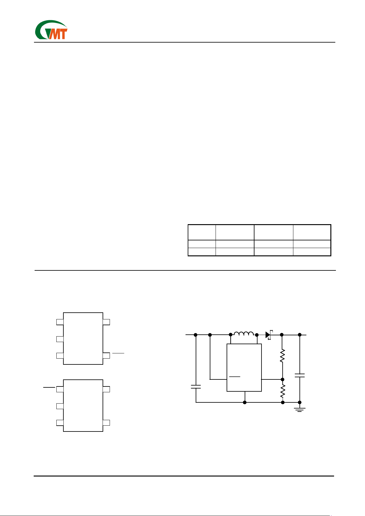
Pin Configuration Typical Application Circuit
G963
VCC
SHDN
SOT23-5
G5111 T11
5
4
1
SW
2
3
GND
FB
VCC
SW
SHDN
FB
GND
G5111
1µF
4.7µF
10µH
62k
V
IN
2.5V to 4.2V
1M
20V
12mA
G963
VCC
SHDN
SOT23-5
G5111 T12
5
4
1
SW
2
3
GND
FB
G963
VCC
SHDN
SOT23-5
G5111 T11
5
4
1
SW
2
3
GND
FB
VCC
SW
SHDN
FB
GND
G5111
1µF
4.7µF
10µH
62k
V
IN
2.5V to 4.2V
1M
20V
12mA
VCC
SW
SHDN
FB
GND
G5111
1µF
4.7µF
10µH
62k
V
IN
2.5V to 4.2V
1M
20V
12mA
G963
VCC
SHDN
SOT23-5
G5111 T12
5
4
1
SW
2
3
GND
FB
Page 2
Ver: 1.1
Oct 02, 2002
TEL: 886-3-5788833
http://www.gmt.com.tw
2
G5111
Global Mixed-mode Technology Inc.
Absolute Maximum Ratings
SW to GND…………………………………..-0.3V to +30V
FB to GND…………… ………………………..-0.3V to V
CC
VCC,
SHDN
to
GND.............................….....-0.3V to +7V
Operating Temperature Range (Note 1) ..-40°C to +85°C
Junction Temperature ......….......….........….........+125°C
Storage Temperature…………........….. –65°C to +150°C
Lead Temperature (Soldering, 10 sec).…………..+300°C
Stress beyond those listed under “Absolute Maximum Rating” may cause permanent damage to the device.
Electrical Characteristics
(VCC = 3.6V,
V
SHDN
= 3.6V, TA =
25°C
)
PARAMETER CONDITIONS MIN TYP MAX UNITS
Input Voltage Range 2.5 6.5 V
Not Switching 20 30 µA
Quiescent Current
V
SHDN
= 0V
0.1 1 µA
FB Comparator Trip Point 1.18 1.2 1.22 V
Output Voltage Line Regulation 2.5V<VIN<6.5V -0.05 %/V
FB Pin Bias Current (Note 2) VFB = 1.2V 30 80 nA
V
FB
> 1V 500 ns
Switch Off Time
V
FB
< 0.6V 1.6 µs
Switch V
DS(ON)
I
SW
= 300mA 250 350 mV
Switch Current Limit 300 350 400 mA
SHDN
Pin Current
0.1 1 µA
SHDN
Input Voltage High
0.9 V
SHDN
Input Voltage Low
0.25 V
Switch Leakage Current Switch Off, VSW = 28V 0.01 5 µA
Note 1: The G5111 are guaranteed to meet performance specifications from 0°C to 85°C. Specifications over the
-40°C to 85°C operating temperature range are assured by design, characterization and correlation with statistical process controls.
Note 2: Bias current flows into the FB pin.
Block Diagram
+
+
VREF
BIAS
SHUTDOWN
LOGIC
C2
SW
L1
SHDN
VCC
C1
R1
R2
VOUT
FB
ERROR
COMP
1.2V
en_sw
GND
PUMP CONTROL
OC
COMP
DRIVER
T
OFF
PULSE
CONTROL
V
OUT
V
IN
+
+
VREF
BIAS
SHUTDOWN
LOGIC
C2
SW
L1
SHDN
VCC
C1
R1
R2
VOUT
FB
ERROR
COMP
1.2V
en_sw
GND
PUMP CONTROL
OC
COMP
DRIVER
T
OFF
PULSE
CONTROL
V
OUT
V
IN
Page 3
Ver: 1.1
Oct 02, 2002
TEL: 886-3-5788833
http://www.gmt.com.tw
3
G5111
Global Mixed-mode Technology Inc.
Typical Performance Characteristics
(VCC=+3.6V, V
SHDN
=+3.6V, L=10µH, TA=25°C, unless otherwise noted.)
Output Voltage vs. Input Voltage
19
19.5
20
20.5
21
2.533.544.555.5
Input Voltage (V)
Output Voltage (V)
Efficiency vs. Load Current
50
55
60
65
70
75
80
85
90
0.1 1 10 100
Load Current (mA)
Efficiency (%)
VIN=2.7V
VIN=3.6V
VIN=4.2V
Quiescent Current vs. Temperature
10
20
30
40
50
-20 0 20 40 60 80 100
Temperature (°C)
Quiescent Current (µA)
VIN=2.7V
VIN=4.2V
Vds_on vs. Temperature
100
200
300
400
500
-20 0 20 40 60 80 100
Temperature (°C)
Switch Vds_on (mV)
VIN=2.7V
VIN=4.2V
Feedback Voltage vs. Temperature
1.18
1.19
1.2
1.21
1.22
-20 0 20 40 60 80 100
Temperature (°C)
Feedback Voltage (V)
VIN=2.7V
VIN=4.2V
Output Voltage vs. Load Current
19
19.5
20
20.5
21
12345678910
Load Current (mA)
Output Voltage (V)
VIN=2.7V
VIN=4.2V
I
OUT
=1mA
I
OUT
=10mA
Page 4

Ver: 1.1
Oct 02, 2002
TEL: 886-3-5788833
http://www.gmt.com.tw
4
G5111
Global Mixed-mode Technology Inc.
Typical Performance Characteristics
(Continued)
FB Bias Current vs. Temperature
15
20
25
30
-20 0 20 40 60 80 100
Temperature (°C)
Feedback Bias Current (nA)
VIN=2.7V
VIN=4.2V
Switch Current Limit vs. Temperature
250
300
350
400
450
-20 0 20 40 60 80 100
Temperature (°C)
Peak Current (mA)
VIN=2.7V
VIN=4.2V
Load Transient
Line Transient
Page 5

Ver: 1.1
Oct 02, 2002
TEL: 886-3-5788833
http://www.gmt.com.tw
5
G5111
Global Mixed-mode Technology Inc.
Pin Description
PIN
T11 T12
NAME FUNCTION
1 4 SW Switch Pin. The drain of the internal NMOS power switch. Connect this pin to inductor.
2 3 GND Ground.
3 5 FB
Feedback Pin. Set the output voltage by selecting values for R1 and R2 (see Block Diagram):
R1 = R2
2.1
V
OUT
-1
4 1
SHDN
Active-Low Shutdown Pin. Tie this pin to logic-high to enable the device or tied it to logic-low
to turn this device off.
5 2 VCC Input Supply Pin. Bypass this pin with a capacitor as close to the device as possible.
Function Description
The G5111 is a boost converter with a NMOS
switch embedded (refer to Block Diagram). The
boost cycle is getting started when FB pin voltage
drop below 1.2V as the NMOS switch turns on.
During the switch on period, the inductor current
ramps up until 350mA current limit is reached. Then
turns the switch off, while the inductor current flows
through external schottky diode, and ramps down to
zero. During the switch off period, the inductor current charges output capacitor and the output voltage
is boosted up. This pumping mechanism continues
cycle by cycle until the FB pin voltage exceed 1.2V
and entering the none switching mode. In this mode,
the G5111 consumes as low as 20uA typically to
save battery power.
Applications Information
Choosing an Inductor
There are several recommended inductors that work
well with the G5111 in Table 1. Use the equations and
recommendations in the next few sections to find the
proper inductance value for your design.
Table 1. Recommended Inductors
PART VALUE((((µH) MAX DCR ((((ΩΩΩΩ) VENDOR
LQH3C4R7
LQH3C100
LQH3C220
4.7
10
22
0.26
0.30
0.92
Murata
www.murata.com
CD43-4R7
CD43-100
CDRH4D18-4R7
CDRH4D18-100
4.7
10
4.7
10
0.11
0.18
0.16
0.20
Sumida
www.sumida.com
DO1608-472
DO1608-103
DO1608-223
4.7
10
22
0.09
0.16
0.37
Coilcraft
www.coilcraft.com
Inductor Selection—Boost Regulator
The appropriate inductance value for the boost regulator application may be calculated from the following
equation. Select a standard inductor close to this
value.
V
OUT-VIN(MIN)+VD
L =
I
LIM
x t
OFF
Where VD = 0.4V (Schottky diode voltage), I
LIM
=
350mA and t
OFF
= 500ns. A larger value can be used
to lightly increase the available output current, but limit
it to about twice the calculating value. When too large
of an inductor will increase the output voltage ripple
without providing much additional output current. In
varying V
IN
condition such as battery power applica-
tions, use the minimum V
IN
value in the above equation. A smaller value can be used to give smaller
physical size, but the inductor current overshoot will
be occurs (see Current Limit Overshoot section).
Inductor Selection—SEPIC Regulator
For a SEPIC regulator using the G5111, the approximate inductance value can be calculated by below
formula. As for the boost inductor selection, a larger or
smaller value can be used.
V
OUT
+ VD
L = 2
I
LIM
x t
OFF
Current Limit Overshoot
The G5111 use a constant off-time control scheme,
the power switch is turned off after the 350mA current
limit is reached. When the current limit is reached and
when the switch actually turns off, there is a 100ns
delay time. During this time, the inductor current exceeds the current limit by a small amount. The formula
below can calculate the peak inductor current.
V
IN(MAX)
- V
SAT
I
PEAK
= I
LIM
+
L
x 100ns
Where V
SAT
= 0.25V (switch saturation voltage). When
the systems with high input voltages and uses smaller
inductance value, the current overshoot will be most
apparent. This overshoot can be useful as it helps
increase the amount of available output current. To
use small inductance value for systems design, the
current limit overshoot can be quite high. Even if it is
internally current limited to 350mA, the power switch of
the G5111 can operate larger currents without any
problem, but the total efficiency will suffer. The I
PEAK
is
keep below 500mA for the G5111 will be obtained
best performance.
Page 6

Ver: 1.1
Oct 02, 2002
TEL: 886-3-5788833
http://www.gmt.com.tw
6
G5111
Global Mixed-mode Technology Inc.
Capacitor Selection
Low ESR (Equivalent Series Resistance) capacitors
should be used at the output to minimize the output
ripple voltage and the peak-to-peak transient voltage.
Multilayer ceramic capacitors (MLCC) are the best
choice, as they have a very low ESR and are available
in very small packages. Their small size makes them a
good match with the G5111’s SOT-23 package. If
solid tantalum capacitors (like the AVX TPS, Sprague
593D families) or OS-CON capacitors are used, they
will occupy more volume than a ceramic ones and the
higher ESR increases the output ripple voltage. Notice
that use a capacitor with a sufficient voltage rating.
A low ESR surface-mount ceramic capacitors also
make a good selection for the input bypass capacitor,
which should be placed as close as possible to the
G5111. A 4.7µF input capacitor is sufficient for most
applications.
Diode Selection
For most G5111 applications, the high switching frequency requires a high-speed rectifier Schottky diodes,
such as the Motorola MBR0530 (0.5A, 30V) with their
low forward voltage drop and fast switching speed, are
recommended. Many different manufacturers make
equivalent parts, but make sure that the component is
rated to operate at least 0.35A. To achieve high efficiency, the average current rating of the Schottky diodes should be greater than the peak switching current. Choose a reverse breakdown voltage greater
than the output voltage.
Lowering Output Voltage Ripple
The G5111 supplies energy to the load in bursts by
ramping up the inductor current, then delivering that
current to the load. To use low ESR capacitors will
help minimize the output ripple voltage, but proper
selection of the inductor and the output capacitor also
plays a big role. If a larger inductance value or a
smaller capacitance value is used, the output ripple
voltage will increase because the capacitor will be
slightly overcharged each burst cycle. To reduce the
output ripple, increase the output capacitance value or
add a 10pF feed-forward capacitor in the feedback
network of the G5111 (see the circuits in the Typical
Applications section). To add this small, inexpensive
10pF capacitor will greatly reduce the output voltage
ripple.
Typical Applications
Boost Converter SEPIC Converter
VCC
SW
SHDN
FB
GND
G5111
C2
22µF
C1
4.7µF
L1
4.7µH
R2
120k
V
IN
2.5V to 4.2V
R1
390k
5V
50mA
D1
L1
10µH
VCC
SW
SHDN
FB
GND
G5111
C2
22µF
C1
4.7µF
R2
270k
V
IN
2.5V to 4.2V
R1
470k
3.3V
60mA
C3
1µF
L1:MURATA LQH3C4R7M24
D1:MOTOROLA MBR0520
L1,L2:MURATA LQH3C100K24
D1:MOTOROLA MBR0520
L2
10µH
D1
VCC
SW
SHDN
FB
GND
G5111
C2
22µF
C1
4.7µF
L1
4.7µH
R2
120k
V
IN
2.5V to 4.2V
R1
390k
5V
50mA
D1
L1
10µH
VCC
SW
SHDN
FB
GND
G5111
C2
22µF
C1
4.7µF
R2
270k
V
IN
2.5V to 4.2V
R1
470k
3.3V
60mA
C3
1µF
L1:MURATA LQH3C4R7M24
D1:MOTOROLA MBR0520
L1,L2:MURATA LQH3C100K24
D1:MOTOROLA MBR0520
L2
10µH
D1
Page 7

Ver: 1.1
Oct 02, 2002
TEL: 886-3-5788833
http://www.gmt.com.tw
7
G5111
Global Mixed-mode Technology Inc.
White LED Driver
R1
30_1%
R2
120k_1%
Dimming Ratio>50:1
Drive 2~8 White LEDs
R3
308k_1%
R4
660k_1%
VBIAS(+3.3V)
PWM Dim
PWM Dimming Control
VH=3.3V
VL=0V
Freq=160~240Hz
D2(Optional)
27V
C2
1µF
D1
MBR0530
L1
10µH/0.5A
SW
VCC
G5111
SHDN
FB
GND
VBAT
2.5V~5.5V
C1
4.7µF
ON/OFF Control
R1
30_1%
R2
120k_1%
Dimming Ratio>50:1
Drive 2~8 White LEDs
R3
308k_1%
R4
660k_1%
VBIAS(+3.3V)
PWM Dim
PWM Dimming Control
VH=3.3V
VL=0V
Freq=160~240Hz
D2(Optional)
27V
C2
1µF
D1
MBR0530
L1
10µH/0.5A
SW
VCC
G5111
SHDN
FB
GND
VBAT
2.5V~5.5V
C1
4.7µF
ON/OFF Control
Page 8

Ver: 1.1
Oct 02, 2002
TEL: 886-3-5788833
http://www.gmt.com.tw
8
G5111
Global Mixed-mode Technology Inc.
Package Information
Note:
1. Package body sizes exclude mold flash protrusions or gate burrs
2. Tolerance ±0.1000 mm (4mil) unless otherwise specified
3. Coplanarity: 0.1000mm
4.
Dimension L is measured in gage plane
DIMENSIONS IN MILLIMETERS
SYMBOLS
MIN NOM MAX
A 1.00 1.10 1.30
A1 0.00 ----- 0.10
A2 0.70 0.80 0.90
b 0.35 0.40 0.50
C 0.10 0.15 0.25
D 2.70 2.90 3.10
E 1.40 1.60 1.80
e ----- 1.90(TYP) -----
e1 ----- 0.95 -----
H 2.60 2.80 3.00
L 0.37 ------ -----
θ
1
1º 5º 9º
Taping Specification
GMT Inc. d oes not assume any responsibility for use of any circuitry described, no circuit patent licenses are implied and GMT Inc. reserves the right at any time without notice to change said circuitry and specifications.
E
e
D
H
θ
1
L
C
b
A2
A1
A
e1
E
e
D
H
θ
1
L
C
b
A2
A1
A
e1
Feed Direction
SOT23-5 Package Orientation
Feed Direction
SOT23-5 Package Orientation
 Loading...