

Datasheet G1-300P-85-2.0, G1-300B-85-2.0, G1-266P-85-1.8, G1-266B-85-1.8, G1-233P-85-1.8 Datasheet (NSC)
...Page 1
© 2000 National Semiconductor Corporation www.national.com
Geode™ GX1 Processor Series Low Power Integrated x86 Solution
General Description
The National Semiconductor®Geode™ GX1 processor
series is a line of integrated processors specifically
designed to power information appliances for entertainment, education, and business. Serving the needs of consumers and business professionals alike, it’s the perfect
solution for IA (information appliance) applications such as
thin clients, interactive set-top boxes, and personal internet
access devices.
The Geode GX1 processorseries is dividedintothreemain
categories as defined by the core operating voltage. Available with core voltages of 2.0V, 1.8V, and 1.6V, it offers
extremely low typical power consumption (1.2W, 1.0W, and
0.8W, respectively) leading to longer battery life and
enabling small form-factor, fanless designs. Typical power
consumption is defined as an average, measured running
Microsoft Windows at 80% Active Idle (Suspend-on-Halt)
with a display resolution of 800x600x8 bpp at 75 Hz.
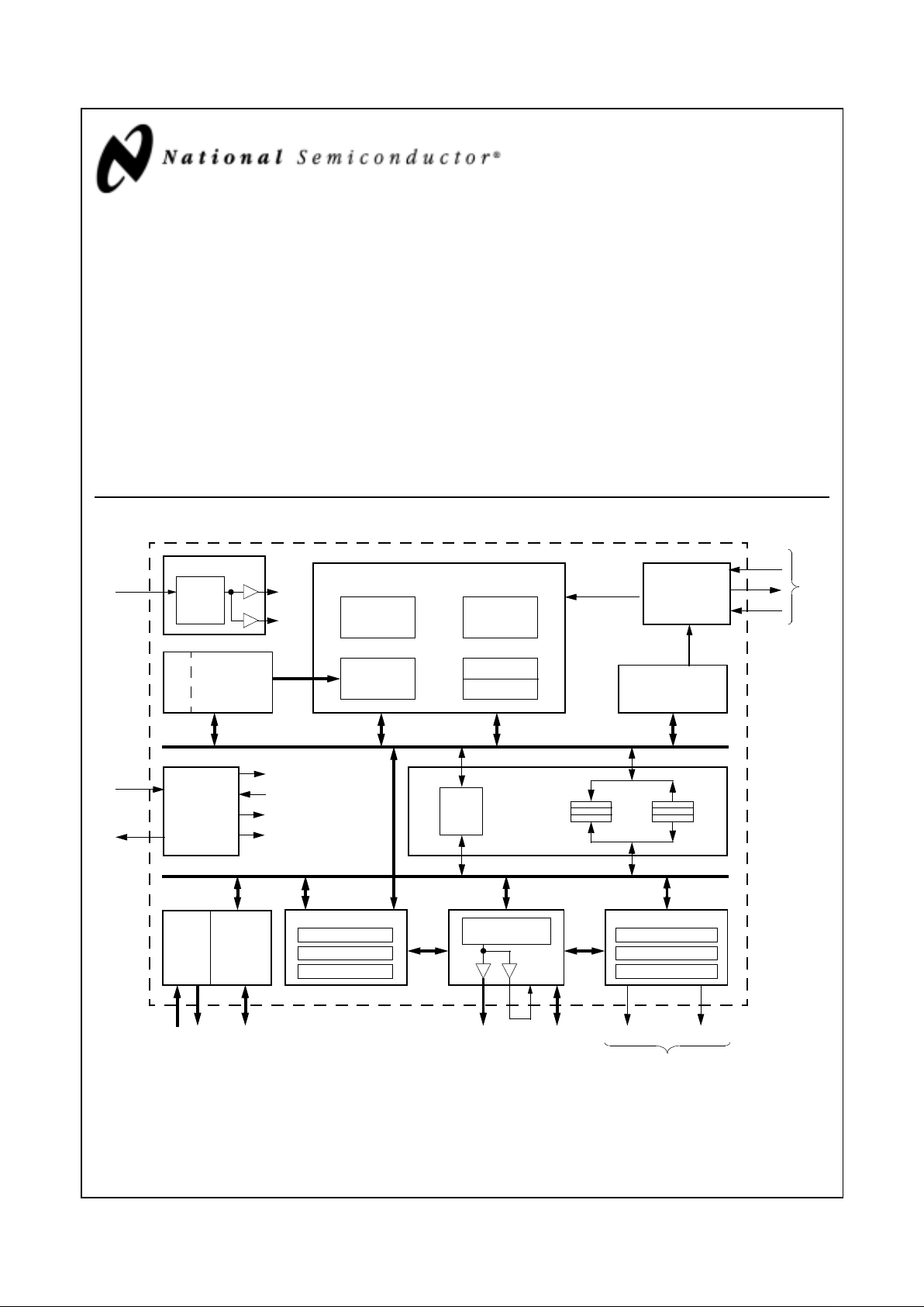
Geode™ GX1 Processor Internal Block Diagram
Interrupt
Floating Point
Clock Module
SYSCLK
Core
X-Bus
x86 Compatible Core
TLB
Instruction
16 KB
Unified L1
Cache
SYSCLK
X-Bus CLK
(128)
FP_Error
INT/NMI
X-Bus
Power
Management
Control
SUSP#
SUSPA#
Core Suspend
Core Acknowledge
X-Bus Suspend
X-Bus Acknowledge
X-Bus (32)
C-Bus (64)
Write
Read
Display Controller
Timing Generator
INTR
IRQ13
3
REQ/GNT
Pairs
PCI 4
SDRAM
Clocks
64-bit RGB YUV
Geode™ Graphics
Scratchpad
Arbiter
SMI#
Geode™ I/O Companio
Clocks
Clocks
Fetch
MMU
Load/Store
Integer
Unit
Unit
Control
Controller
Palette RAM
Compression Buffer
2D Accelerator
ROP Unit
BLT Engine
VGA
Buffers
Buffers
SDRAM
Bus
Arbiter
PCI Host
Controller
multiplied
by “A”
divide by “B”
Companion Interface
April 2000
Geode™ GX1 Processor Series
Low Power Integrated x86 Solution
National Semiconductor and V irtual System Architecture are registered trademarks of National Semiconductor Corporation.
Geode, WebPAD, and VSA, are trademarks of National Semiconductor Corporation.
For a complete listing of National Semiconductor trademarks, please visit www.national.com/trademarks.
Page 2
www.national.com 2 Revision 1.0
Geode™ GX1 Processor Series
While the x86 core provides maximum compatibility with
the vast amount of Internet content available, the intelligent
integration of several other functions, such as audio and
graphics, offers a true system-levelmultimedia solution.
The Geode GX1 processor core is a proven x86 design
that offers competitive performance. It contains integer and
floating point execution units based on sixth-generation
technology. The integer core contains a single, five-stage
execution pipeline and offers advanced features such as
operand forwarding, branch target buffers, and extensive
write buffering. Accesses to the 16 KB write-back L1 cache
are dynamically reordered to eliminate pipeline stalls when
fetching operands.
In addition to the advanced CPU features, the GX1 processor integrates a host of functions typically implemented
with external components. A full function graphics accelerator contains a VGA (video graphics array) controller, bitBLT engine, and a ROP (raster operations) unit for
complete GUI (Graphical User Interface) acceleration
under most operating systems. A display controller contains additional video buffering to enable >30 fps MPEG1
playback and video overlay when used with a National
Semiconductor Geode I/O or graphics companion chip
(e.g., CS5530 or CS9211). Graphics and system memory
accesses are supported by a tightly coupled SDRAM controller which eliminates the need for an external L2 cache.
A PCI host controller supports up to three bus masters for
additional connectivity and multimedia capabilities.
The GX1 processor also incorporates Vir tual System
Architecture
®
(VSA™) technology. VSA technology
enables the XpressGRAPHICS and XpressAUDIO subsystems. Software handlers are available that provide full
compatibility for industry standard VGA and 16-bit audio
functions that are transparent at the operating system level.
Together the National Semiconductor I/O companion and
GX1 processor Geode devices provide a scalable, flexible,
low-power, system-level solution well suited for a wide
array of information appliances ranging from hand-held
personal information access devices to digital set-top
boxes and thin clients.
Features
General Features
Packaging:
— 352-Terminal Ball Grid Array (BGA) or
— 320-Pin Staggered Pin Grid Array (SPGA)
0.18-micron four layer metal CMOS process
Split rail design:
— Available 1.6V, 1.8V, or 2.0V core
— 3.3V I/O interface
Fully static design
Low Typical Power Consumption:
— 0.8W @ 1.6V/200 MHz
— 1.2W @ 2.0V/300 MHz
Note: Typical power consumption is defined as an aver-
age, measured running Windows at 80% Active
Idle (Suspend-on-Halt) with a display resolution of
800x600x8 bpp @ 75 Hz.
Speeds offered up to 300 MHz
Unified Memory Architecture
— Frame buffer and video memory reside in main
memory
— Minimizes PCB (Printed Circuit Board) area require-
ments
— Reduces system cost
Compatiblewith multiple Geode I/O companion devices
provided by National Semiconductor
32-Bit x86 Processor
Supports Intel’s MMX instruction set extension for the
acceleration of multimedia applications
16 KB unified L1 cache
Six-stage pipelined integer unit
Integrated Floating Point Unit (FPU)
Memory Management Unit (MMU) adheres to standard
paging mechanisms and optimizes code fetch performance:
— Load-store reordering gives priority to memory reads
— Memory-read bypassing eliminates unnecessary or
redundant memor y reads
Re-entrant System Management Mode (SMM)
enhanced for VSA technology
Page 3
Revision 1.0 3 www.national.com
Geode™ GX1 Processor Series
Flexible Power Management
Supports a wide variety of standards:
— APM (Advanced PowerManagement) for Legacy
power management
— ACPI (Advanced Configuration and Power Interface)
for Windows power management
– Direct support forall standard processor (C0-C4)
states
— OnNOW design initiative compliant
Supports a wide variety of hardware and software
controlled modes:
— Active Idle (core-only stopped, display active)
— Standby (core and all integrated functions halted)
— Sleep (core and integrated functions halted and all
external clocks stopped)
— Suspend Modulation (automatic throttling of CPU
core via Geode I/O or graphics companion chip)
– Programmableduty cycle for optimal performance/
thermal balancing
— Several dedicated and programmable wake-up
events (via Geode I/O or graphics companion chip)
PCI Host Controller
Several arbitration schemes supported
Directlysupports up to three PCI bus masters,more with
external logic
Synchronous to CPU core
Allows external PCI master accesses to main memory
concurrent with CPU accesses to L1 cache
Virtual Systems Architecture Technology
Innovative architecture allowing OS independent (software) virtualization of hardware functions
Provides XpressGRAPHICS subsystem:
— High performance legacy VGA core compatibility
Note: The GUI acceleration is pure hardware.
Provides 16-bit XpressAUDIO subsystem:
— 16-bit stereo FM synthesis
—OPL3emulation
— Supports MPU-401 MIDIinterface
— Hardware assist provided v ia Geode I/O companion
chip
Additional hardware functions can be supported as
needed
2D Graphics Accelerator
Accelerates BitBLTs, line draw, text:
— Bresenham vector engine
Supports all 256 RasterOperations (ROPs)
Supports transparent BLTs and page flipping for
Microsoft’s DirectDraw
Runs at core clock frequency
Full VGA and VESA mode support
Special "driver level” instructions utilize internal
scratchpad for enhanced performance
Display Controller
Display Compression Technology (DCT) architecture
greatly reduces memory bandwidth consumption of
display refresh
Supports a separate video buffer and data path to
enable video acceleration in Geode I/O and graphics
companion chips
Internal palette RAM for gamma correction
Direct interface to GeodeI/O and graphics companion
chips for CRT and TFT flat panel support eliminates the
need for an external RAMDAC
Hardware cursor
Supports up to 1280x1024x8 bpp and 1024x768x16 bpp
XpressRAM
SDRAM interface tightly coupled to CPU coreand
graphics subsystem for maximum efficiency
64-Bit wide memory bus
Support for:
— Two 168-pin unbuffered DIMMs
— Up to 16 simultaneously open banks
— 16-byte reads (burst length of two)
— Up to 512MB total memory supported
Diverse Operating System Support
Microsoft’s Windows 2000, Windows 95, Windows 98,
and Windows NT in non PC applications; along with
Windows CE and Windows NTE
WindRiverSystem’s VxWorks
QNX Software Systems’ QNX
Linux
Page 4

www.national.com 4 Revision 1.0
Geode™ GX1 Processor Series
Table of Contents
1.0 ArchitectureOverview..............................................10
1.1 INTEGERUNIT ............................................................11
1.2 FLOATINGPOINTUNIT .....................................................11
1.3 WRITE-BACKCACHEUNIT ..................................................11
1.4 MEMORYMANAGEMENTUNIT...............................................11
1.5 INTERNALBUSINTERFACEUNIT.............................................11
1.6 INTEGRATED FUNCTIONS . . . . ..............................................12
1.6.1 Graphics Accelerator . . . ..............................................12
1.6.2 DisplayController....................................................12
1.6.3 XpressRAMMemorySubsystem ........................................12
1.6.4 PCIController.......................................................12
1.7 GEODEGX1/CS5530SYSTEMDESIGNS .......................................13
1.7.1 ReferenceDesigns...................................................16
2.0 SignalDefinitions..................................................19
2.1 PINASSIGNMENTS ........................................................20
2.2 SIGNALDESCRIPTIONS ....................................................31
2.2.1 SystemInterfaceSignals ..............................................31
2.2.2 PCIInterfaceSignals .................................................33
2.2.3 MemoryControllerInterfaceSignals .....................................36
2.2.4 VideoInterfaceSignals ...............................................37
2.2.5 Power,Ground,andNoConnectSignals..................................39
2.2.6 InternalTestandMeasurementSignals...................................39
3.0 ProcessorProgramming............................................41
3.1 COREPROCESSORINITIALIZATION ..........................................41
3.2 INSTRUCTIONSETOVERVIEW...............................................42
3.2.1 LockPrefix .........................................................42
3.3 REGISTERSETS...........................................................43
3.3.1 ApplicationRegisterSet...............................................43
3.3.1.1 GeneralPurposeRegisters ............................................43
3.3.1.2 SegmentRegisters...................................................45
3.3.1.3 InstructionPointerRegister ............................................45
3.3.1.4 EFLAGSRegister....................................................46
3.3.2 SystemRegisterSet .................................................47
3.3.2.1 ControlRegisters....................................................48
3.3.2.2 ConfigurationRegisters...............................................50
3.3.2.3 DebugRegisters.....................................................55
3.3.2.4 TLBTestRegisters...................................................57
3.3.2.5 CacheTestRegisters.................................................59
3.3.3 ModelSpecificRegister ...............................................62
3.3.4 TimeStampCounter .................................................62
3.4 ADDRESSSPACES.........................................................63
3.4.1 I/OAddressSpace...................................................63
3.4.2 MemoryAddressSpace...............................................64
Page 5

Revision 1.0 5 www.national.com
Geode™ GX1 Processor Series
Table of Contents (Continued)
3.5 OFFSET,SEGMENT,ANDPAGINGMECHANISMS ...............................64
3.5.1 Offset Mechanism . . . . . ..............................................64
3.5.2 SegmentMechanisms ................................................66
3.5.2.1 RealModeSegmentMechanism........................................66
3.5.2.2 Virtual8086ModeSegmentMechanism..................................66
3.5.2.3 SegmentMechanisminProtectedMode..................................67
3.5.2.4 SegmentSelectors...................................................67
3.5.3 Descriptors.........................................................70
3.5.3.1 GlobalandLocalDescriptorTableRegisters...............................70
3.5.3.2 SegmentDescriptors.................................................70
3.5.3.3 Task,Gate,Interrupt,andApplicationandSystemDescriptors.................71
3.5.4 PagingMechanism...................................................77
3.6 INTERRUPTSANDEXCEPTIONS .............................................79
3.6.1 Interrupts ..........................................................79
3.6.2 Exceptions .........................................................79
3.6.3 InterruptVectors.....................................................80
3.6.3.1 InterruptVectorAssignments...........................................80
3.6.3.2 InterruptDescriptorTable..............................................80
3.6.4 InterruptandExceptionPriorities........................................81
3.6.5 ExceptionsinRealMode ..............................................82
3.6.6 ErrorCodes ........................................................82
3.7 SYSTEMMANAGEMENTMODE ..............................................83
3.7.1 SMMOperation .....................................................84
3.7.2 SMI#Pin...........................................................85
3.7.3 SMMConfigurationRegisters ..........................................85
3.7.4 SMMMemorySpaceHeader...........................................85
3.7.5 SMMInstructions ....................................................87
3.7.6 SMMMemorySpace .................................................88
3.7.7 SMIGenerationforVirtualVGA .........................................88
3.7.8 SMMServiceRoutineExecution ........................................88
3.7.9 SMINesting ........................................................88
3.7.9.1 CPUStatesRelatedtoSMMandSuspendMode...........................90
3.8 HALTANDSHUTDOWN .....................................................91
3.9 PROTECTION .............................................................91
3.9.1 PrivilegeLevels .....................................................91
3.9.2 I/OPrivilegeLevels ..................................................91
3.9.3 PrivilegeLevelTransfers ..............................................92
3.9.3.1 Gates.............................................................92
3.9.4 InitializationandTransitiontoProtectedMode..............................93
3.10 VIRTUAL8086MODE .......................................................93
3.10.1 MemoryAddressing..................................................93
3.10.2 Protection ..........................................................93
3.10.3 Interrupt Handling . . . . . . ..............................................93
3.10.4 EnteringandLeavingVirtual8086Mode..................................93
3.11 FLOATINGPOINTUNITOPERATIONS .........................................94
3.11.1 FPURegisterSet ....................................................94
3.11.2 FPUTagWordRegister ...............................................94
3.11.3 FPUStatusRegister .................................................94
3.11.4 FPUModeControlRegister............................................94
Page 6

www.national.com # Revision 1.0
Geode™ GX1 Processor Series
Table of Contents (Continued)
4.0 Integrated Functions . . . . . . . . . . . . . . . . . . . . . . . . . . . . . . . . . . . . . . . . . . . . . . . 96
4.1 INTEGRATED FUNCTIONS PROGRAMMING INTERFACE . . . . . . . . .................97
4.1.1 Graphics Control Register . . . . . . . . . . . . . . . ..............................97
4.1.2 ControlRegisters ....................................................99
4.1.3 Graphics Memory . . . . . . ..............................................99
4.1.4 ScratchpadRAM ...................................................100
4.1.4.1 InitializationofScratchpadRAM........................................100
4.1.4.2 ScratchpadRAMUtilization...........................................100
4.1.4.3 BLTBuffer.........................................................100
4.1.5 DisplayDriverInstructions ............................................102
4.1.6 CPU_READ/CPU_WRITEInstructions ..................................102
4.2 INTERNALBUSINTERFACEUNIT............................................103
4.2.1 FPUErrorSupport ..................................................103
4.2.2 A20MSupport .....................................................103
4.2.3 SMIGeneration ....................................................103
4.2.4 640KBto1MBRegion ..............................................103
4.2.5 InternalBusInterfaceUnitRegisters ....................................104
4.3 MEMORYCONTROLLER ...................................................107
4.3.1 MemoryArrayConfiguration ..........................................108
4.3.2 MemoryOrganizations...............................................109
4.3.3 SDRAMCommands.................................................110
4.3.3.1 SDRAMInitializationSequence........................................111
4.3.4 MemoryControllerRegisterDescription .................................112
4.3.5 AddressTranslation .................................................117
4.3.5.1 HighOrderInterleaving ..............................................117
4.3.5.2 AutoLowOrderInterleaving...........................................117
4.3.5.3 PhysicalAddresstoDRAMAddressConversion...........................117
4.3.6 MemoryCycles ....................................................120
4.3.7 SDRAMInterfaceClocking............................................123
4.4 GRAPHICSPIPELINE ......................................................125
4.4.1 BitBLT/VectorEngine ................................................125
4.4.2 Master/SlaveRegisters ..............................................126
4.4.3 PatternGeneration..................................................126
4.4.3.1 MonochromePatterns ...............................................127
4.4.3.2 DitherPatterns.....................................................127
4.4.3.3 ColorPatterns......................................................128
4.4.4 SourceExpansion ..................................................128
4.4.5 RasterOperations ..................................................128
4.4.6 Graphics Pipeline Register Descriptions . . . . .............................129
Page 7

Revision 1.0 7 www.national.com
Geode™ GX1 Processor Series
Table of Contents (Continued)
4.5 DISPLAYCONTROLLER....................................................134
4.5.1 DisplayFIFO ......................................................135
4.5.2 CompressionTechnology.............................................135
4.5.3 HardwareCursor ...................................................136
4.5.4 DisplayTimingGenerator.............................................136
4.5.5 DitherandFrameRateModulation .....................................136
4.5.6 DisplayModes .....................................................136
4.5.7 Graphics Memory Map . . .............................................140
4.5.7.1 DCMemoryOrganizationRegisters.....................................140
4.5.7.2 FrameBufferandCompressionBufferOrganization........................140
4.5.7.3 VGADisplaySupport................................................141
4.5.8 DisplayControllerRegisters...........................................141
4.5.8.1 ConfigurationandStatusRegisters.....................................144
4.5.9 MemoryOrganizationRegisters........................................148
4.5.10 TimingRegisters ...................................................150
4.5.11 CursorPositionandMiscellaneousRegisters .............................153
4.5.12 PaletteAccessRegisters .............................................154
4.5.13 FIFODiagnosticRegisters ............................................155
4.5.14 CS5530DisplayControllerInterface ....................................156
4.5.14.1 CS5530VideoPortDataTransfer ......................................157
4.6 VIRTUALVGASUBSYSTEM.................................................158
4.6.1 TraditionalVGAHardware ............................................158
4.6.1.1 VGAMemoryOrganization............................................159
4.6.1.2 VGAFrontEnd.....................................................160
4.6.1.3 AddressMapping...................................................160
4.6.1.4 VideoRefresh......................................................160
4.6.1.5 VGAVideoBIOS ...................................................161
4.6.2 VirtualVGA .......................................................161
4.6.2.1 DatapathElements..................................................161
4.6.2.2 GX1VGAHardware.................................................162
4.6.2.3 SMIGeneration ....................................................162
4.6.2.4 VGARangeDetection ...............................................162
4.6.2.5 VGASequencer....................................................162
4.6.2.6 VGAWrite/ReadPath................................................162
4.6.2.7 VGAAddressGenerator..............................................162
4.6.2.8 VGAMemory ......................................................163
4.6.3 VGAConfigurationRegisters ..........................................163
4.6.4 VirtualVGARegisterDescriptions ......................................165
4.7 PCICONTROLLER ........................................................167
4.7.1 X-BusPCISlave....................................................167
4.7.2 X-BusPCIMaster ..................................................167
4.7.3 PCIArbiter ........................................................167
4.7.4 GeneratingConfigurationCycles .......................................167
4.7.5 GeneratingSpecialCycles............................................167
4.7.6 PCIConfigurationSpaceControlRegisters...............................168
4.7.7 PCIConfigurationSpaceRegisters .....................................169
4.7.8 PCICycles ........................................................174
4.7.8.1 PCIReadTransaction................................................174
4.7.8.2 PCIWriteTransaction................................................175
4.7.8.3 PCIArbitration .....................................................176
4.7.8.4 PCIHaltCommand..................................................176
Page 8

www.national.com # Revision 1.0
Geode™ GX1 Processor Series
Table of Contents (Continued)
5.0 PowerManagement ...............................................177
5.1 POWERMANAGEMENTFEATURES ..........................................177
5.1.1 SystemManagementMode...........................................177
5.1.2 Suspend-on-Halt ...................................................177
5.1.3 CPUSuspend .....................................................177
5.1.3.1 SuspendModulationforThermalManagement............................178
5.1.3.2 SuspendModulationforPowerManagement..............................178
5.1.4 3VoltSuspend .....................................................178
5.1.5 GX1ProcessorSerialBus ............................................178
5.1.6 AdvancedPowerManagement(APM)Support ............................178
5.2 SUSPENDMODESANDBUSCYCLES ........................................179
5.2.1 TimingDiagramforSuspend-on-Halt....................................179
5.2.2 InitiatingSuspendwithSUSP# ........................................180
5.2.3 Stopping the Input Clock .............................................181
5.2.4 SerialPacketTransmission ...........................................181
5.3 POWERMANAGEMENTREGISTERS .........................................182
6.0 ElectricalSpecifications............................................185
6.1 PARTNUMBERS/PERFORMANCECHARACTERISTICS..........................185
6.2 ELECTRICALCONNECTIONS ...............................................186
6.2.1 Power/GroundConnectionsandDecoupling ..............................186
6.2.1.1 PowerPlanes......................................................186
6.2.2 NC-DesignatedPins.................................................188
6.2.3 Pull-UpandPull-DownResistors.......................................188
6.2.4 UnusedInputPins ..................................................188
6.3 ABSOLUTEMAXIMUMRATINGS.............................................189
6.4 RECOMMENDEDOPERATINGCONDITIONS...................................190
6.5 DCCHARACTERISTICS ....................................................191
6.5.1 Input/OutputDCCharacteristics .......................................191
6.5.2 DCCurrent........................................................191
6.5.2.1 DefinitionofCPUPowerStates........................................191
6.5.2.2 Definition and Measurement Techniques of CPU Current Parameters. . . . . . . . . . .191
6.5.2.3 Definitionof System Conditions for Measuring “On” Parameters. . . . . . . . . . . . . . . 192
6.5.2.4 DCCurrentMeasurements............................................193
6.6 I/O CURRENT DE-RATING CURVE . . . . . . . . . . . . . . .............................196
6.6.1 DisplayResolution ..................................................196
6.6.2 MemorySpeed.....................................................196
6.6.3 I/OCurrentDe-ratingCurve...........................................196
6.7 ACCHARACTERISTICS ....................................................197
7.0 PackageSpecifications............................................207
7.1 THERMALCHARACTERISTICS ..............................................207
7.1.1 HeatsinkConsiderations .............................................208
7.2 MECHANICALPACKAGEOUTLINES..........................................210
Page 9

Revision 1.0 9 www.national.com
Geode™ GX1 Processor Series
Table of Contents (Continued)
8.0 InstructionSet....................................................213
8.1 GENERALINSTRUCTIONSETFORMAT.......................................213
8.1.1 Prefix(Optional) ...................................................214
8.1.2 Opcode...........................................................214
8.1.2.1 wField(OperandSize)...............................................214
8.1.2.2 dField(OperandDirection) ...........................................214
8.1.2.3 sField(ImmediateDataFieldSize).....................................215
8.1.2.4 eeeField(MOV-InstructionRegisterSelection)............................215
8.1.3 modandr/mByte(MemoryAddressing) .................................215
8.1.4 regField..........................................................216
8.1.4.1 sreg2Field(ES,CS,SS,DSRegisterSelection)...........................216
8.1.4.2 sreg3Field(FSandGSSegmentRegisterSelection).......................216
8.1.5 s-i-bByte(Scale,Indexing,Base) ......................................216
8.1.5.1 ssField(ScaleSelection).............................................216
8.1.5.2 indexField(IndexSelection) ..........................................217
8.1.5.3 BaseField(s-i-bPresent).............................................217
8.2 CPUIDINSTRUCTION......................................................218
8.2.1 Standard CPUID Levels . .............................................218
8.2.1.1 CPUIDInstructionwithEAX=00000000h...............................218
8.2.1.2 CPUIDInstructionwithEAX=00000001h...............................219
8.2.1.3 CPUIDInstructionwithEAX=00000002h...............................219
8.2.2 ExtendedCPUIDLevels..............................................220
8.2.2.1 CPUIDInstructionwithEAX=80000000h...............................220
8.2.2.2 CPUIDInstructionwithEAX=80000001h...............................220
8.2.2.3 CPUID Instruction with EAX = 8000 0002h, 80000003h, 8000 0004h . . . . . . . . . .221
8.2.2.4 CPUIDInstructionwithEAX=80000005h...............................221
8.3 PROCESSORCOREINSTRUCTIONSET ......................................222
8.3.1 Opcodes ..........................................................222
8.3.2 ClockCounts ......................................................222
8.3.3 Flags ............................................................222
8.4 FPUINSTRUCTIONSET....................................................234
8.5 MMXINSTRUCTIONSET ...................................................239
8.6 EXTENDEDMMXINSTRUCTIONSET.........................................244
Appendix A Support Documentation . . . . . . . . . . . . . . . . . . . . . . . . . . . . . . . . . . . . 246
A.1 ORDERINFORMATION ....................................................246
A.2 DATABOOKREVISIONHISTORY ............................................246
Page 10
www.national.com 10 Revision 1.0
Geode™ GX1 Processor Series
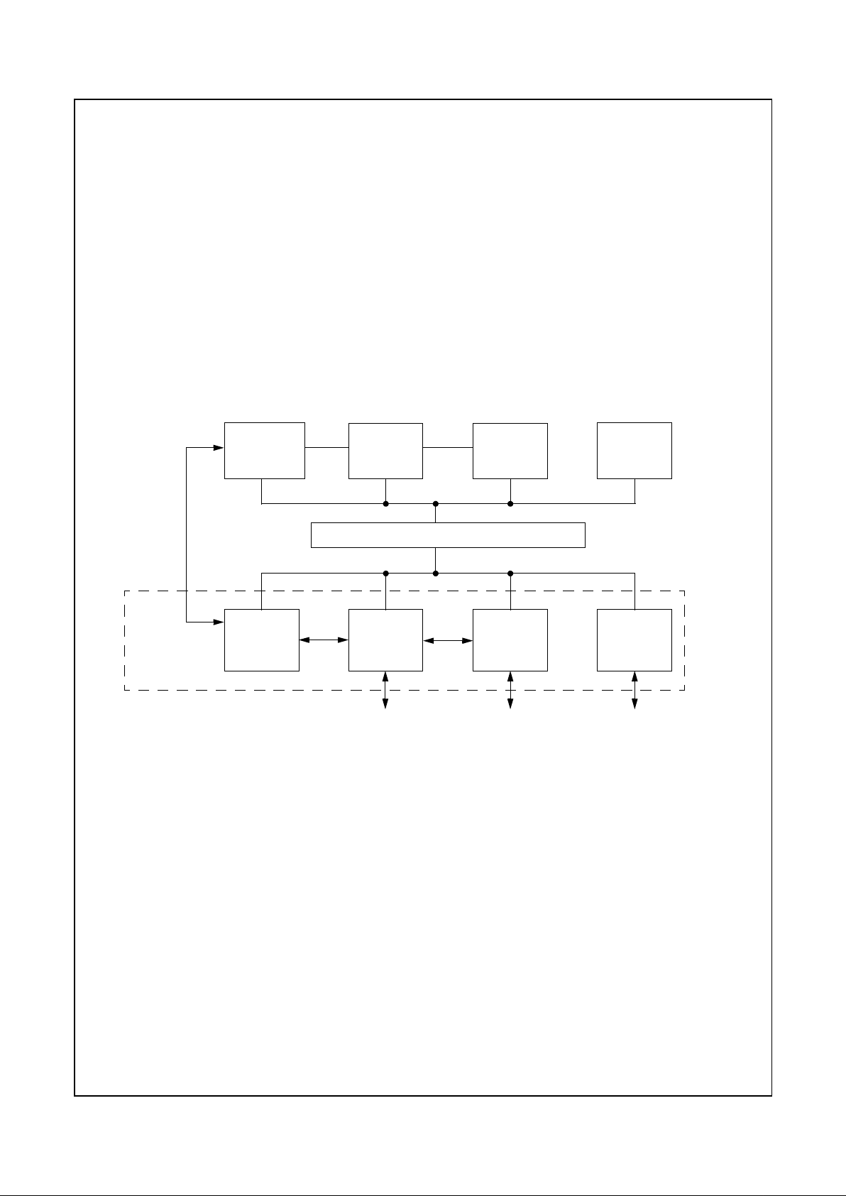
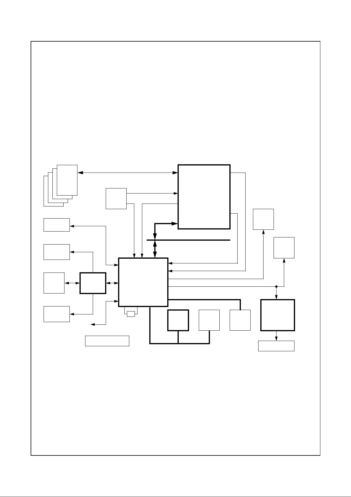
1.0 Architecture Overview
The Geode GX1 processor series represents the sixth generation of x 86-compatible 32-bit processors with sixth-generation features. The decoupled load/store unit allows
reordering of load/store traffic to achieve higher performance. Other features include single-cycle execution, single-cycle instruction decode, 16 KB write-back cache, and
clock rates up to 300MHz. These features are madepossible by theuse of advanced-process technologies and pipelining.
The GX1 processor has low power consumption at all clock
frequencies. Where additional power savings are required,
designers can make use of Suspend Mode, Stop Clock
capability, and SystemManagement Mode (SMM).
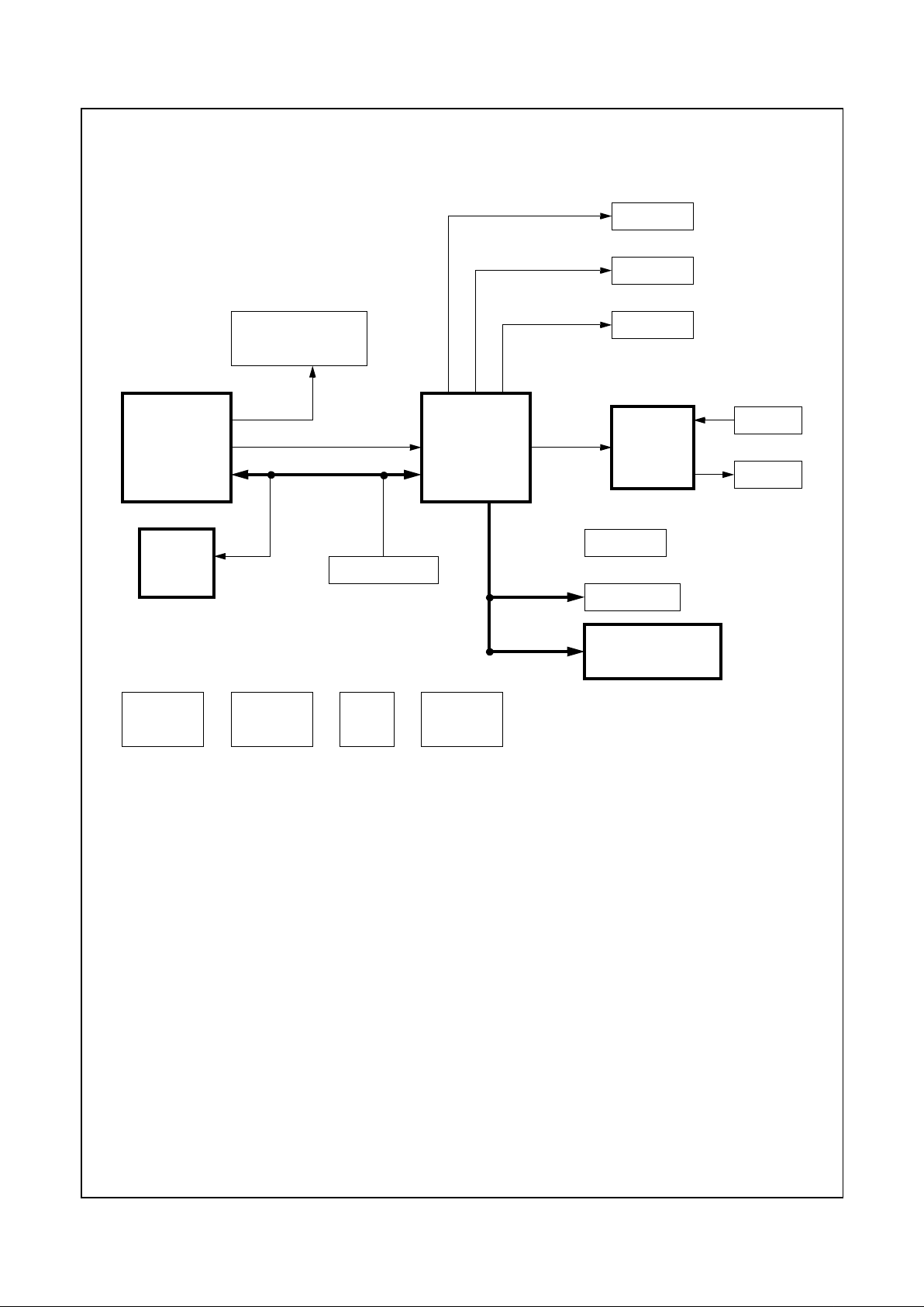
The GX1 processor is divided into major functional blocks
(as shown in Figure 1-1):
• Integer Unit
• Floating Point Unit (FPU)
• Write-Back Cache Unit
• Memory ManagementUnit (MMU)
• Internal Bus Interface Unit
• Integrated Functions
Instructions are executed in the integer unit and in the floating point unit. The cache unit stores the mostrecently used
data and instructions and providesfast access to this information for the integer and floating point units.
Figure 1-1. Internal Block Diagram
Write-Back
Unit
FPU
Internal Bus Interface Unit
Graphics Memory Display PCI
SDRAM Port CS5530
PCI Bus
Integer
Cache Unit
Integrated
Functions
MMU
(CRT/LCD TFT)
X-Bus
Pipeline Controller Controller Controller
C-Bus
Page 11

Revision 1.0 11 www.national.com
Geode™ GX1 Processor Series
Architecture Overview (Continued)
1.1 INTEGER UNIT
The integer unit consists of:
• Instruction Buffer
• Instruction Fetch
• Instruction Decoder and Execution
The pipelined integer unit fetches, decodes, and executes
x86 instructions through the use of a five-stage integer
pipeline.
The instruction fetch pipeline stage generates, from the onchip cache, a continuous high-speed instruction stream for
use by the processor. Up to 128 bits of code are read during a single clock cycle.
Branch prediction logic within the prefetch unit generates a
predicted target address for unconditional or conditional
branch instructions. When a branch instruction is detected,
the instruction fetch stage starts loading instructions at the
predicted address within a single clock cycle. Up to 48
bytes of code are queued prior to the instruction decode
stage.
The instruction decode stage evaluates the code stream
provided by the instruction fetch stage and determines the
number of bytes in each instruction and the instruction
type. Instructions are processed and decoded at a maximum rate of one instruction per clock.
The address calculation function is pipelined and contains
two stages, AC1 and AC2. If the instruction refers to a
memory operand, AC1 calculates a linearmemory address
for the instruction.
The AC2 stage performs any required memory management functions, cache accesses, and register file
accesses. If a floating point instruction is detected by AC2,
the instruction is sent to the floating point unit for processing.
The execution stage, under control of microcode, executes
instructions using the operands provided by the address
calculation stage.
Write-back, the last stage of the integer unit, updates the
register file within theinteger unit or writes to the load/store
unit within the memory management unit.
1.2 FLOATING POINT UNIT
The floating point unit (FPU) interfaces to the integer unit
and the cache unit through a 64-bit bus. The FPU is x87instruction-set compatible and adheres to the IEEE-754
standard. Because almost all applications that contain FPU
instructions also contain integer instructions, the GX1 processor’s FPU achieves high performance by completing
integer and FPU operations in parallel.
FPU instructions are dispatched to the pipeline within the
integer unit. The address calculation stage of the pipeline
checks for memory management exceptions and accesses
memory operands for use by the FPU. Once the instructions and operands have been provided to the FPU, the
FPU completes instruction execution independently of the
integer unit.
1.3 WRITE-BACK CACHE UNIT
The 16 KB write-back unified (data/instruction) cache is
configured as four-way set associative. The cache stores
up to 16 KB of code and data in 1024 cache lines.
The GX1 processor provides the ability to allocate a portion
of the L1 cache as a scratchpad, which is used to accelerate the Virtual Systems Architecture technology algorithms
as well as for some graphics operations.
1.4 MEMORY MANAGEMENT UNIT
The memory management unit (MMU) translates the linear
address supplied by the integer unit into a physical address
to be used by the cache unit and the internal bus interface
unit. Memory management procedures are x86-compatible, adhering to standard paging mechanisms.
The M MU also contains a load/store unit that is responsible
for scheduling cache and external memory accesses. The
load/store unit incorporates two performance-enhancing
features:
• Load-store reordering that gives memory reads
required by the integer unit a priority over writes to
external memory .
• Memory-read bypassing that eliminates unnecessary
memory reads by using valid data from the execution
unit.
1.5 INTERNAL BUS INTERFACE UNIT
The internal bus interface unit provides a bridge from the
GX1 processor to the integrated system functions (i.e.,
memory subsystem, display controller, graphics pipeline)
and the PCI bus interface.
When external memory access is required, the physical
address is calculated by the memory management unit and
then passed to the internal bus interface unit, which translatesthecycletoanX-Buscycle(theX-Busisaproprietary
internal bus which provides a common interface for all of
the integrated functions). The X-Bus memory cycle is arbitrated between other pending X-Bus memory requests to
the SDRAM controller before completing.
In addition, the internal bus interface unit provides configuration control for up to 20 different regions within system
memory with separate controls for read access, write
access, cacheability, and PCI access.
Page 12

www.national.com 12 Revision 1.0
Geode™ GX1 Processor Series
Architecture Overview (Continued)
1.6 INTEGRATED FUNCTIONS
The GX1 processor integrates the following functions traditionally implemented using external devices:
• High-performance 2D graphics accelerator
• Separate CRT and TFT control from the display
controller
• SDRAM memory controller
• PCI bridge
The processor has also been enhanced to support VSA
technology implementation.
The GX1 processor implements a Unified Memory Architecture (UMA). By using DCT (Display Compression Technology) architecture, the performance degradation inherent
in traditional UMA systems is eliminated.
1.6.1 Graphics Accelerator
The graphics accelerator is a full-featured GUI accelerator.
The graphics pipeline implements a bitBLT engine for
frame buffer bitBLTs and rectangular fills. Additional
instructions in the integer unit may be processed, as the
bitBLT engine assists the CPUin the bitBLToperations that
take place between system memory and the frame buffer.
This combination of hardware and software is used by the
display driver to provide very fast bidirectional transfers
between system memory and the frame buffer. The bitBLT
engine also draws randomly oriented vectors, and scanlines for polygon fill. All of the pipeline operations described
in the following list can be applied to any bitBLT operation.
• Pattern Memory: Renderwith 8x8 dither, 8x8 monochrome, or 8x1 color pattern.
• Color Expansion: Expand monochrome bitmaps to full
depth 8- or 16-bit colors.
• Transparency: Suppresses drawing of background
pixels for transparent text.
• Raster Operations: Boolean operation combines
source, destination, and pattern bitmaps.
1.6.2 Display Controller
The display port is a direct interface to the Geode I/O companion (i.e., CS5530) which drives a TFT flat panel display,
LCD panel, or a CRT display.
The display controller (video generator) retrieves image
data from the frame buffer, performs a color-look-up if
required, inserts the cursor overlay into the pixel stream,
generates display timing, and formats the pixel data for output to a variety of display devices. The display controller
contains DCT architecture that allows the GX1 processor
to refresh the display from a compressed copy of the frame
buffer. DCT architecture typically decreases the screen
refresh bandwidth requirement by a factor of 15 to 20, minimizing bandwidth contention.
1.6.3 XpressRAM Memory Subsystem
The memory controller drives a 64-bit SDRAM port directly.
The SDRAM memory array contains both the main system
memory and the graphics frame buffer. Up to four module
banks of SDRAM are supported. Each module bank can
havetwo or four component banks depending on the memory size and organization. The maximum configuration is
four module banks with four component banks, each providing a total of 16 open banks. The maximum memory
size is 512 MB.
The memory controller handles multiple requests for memory data from the GX1 processor, the graphics accelerator
and the display controller. The memory controller contains
extensive buffering logic that helps minimize contention for
memory bandwidth between graphics and CPU requests.
The memory controller cooperates with the internal bus
controller to determinethe cacheability of all memory references.
1.6.4 PCI Controller
The GX1 processor incorporates a full-function PCI interface module that includes the PCI arbiter. All accesses to
external I/O devices are sent over the PCI bus, although
most memory accesses are serviced by the SDRAM controller. The internal bus interface unit contains address
mapping logic that determines if memory accessesare targetedfortheSDRAMorforthePCIbus.ThePCIbusina
GX1 based system is 3.3 volt only. Do not connect 5 volt
deviceson this bus.
Page 13
Revision 1.0 13 www.national.com
Geode™ GX1 Processor Series
Architecture Overview (Continued)
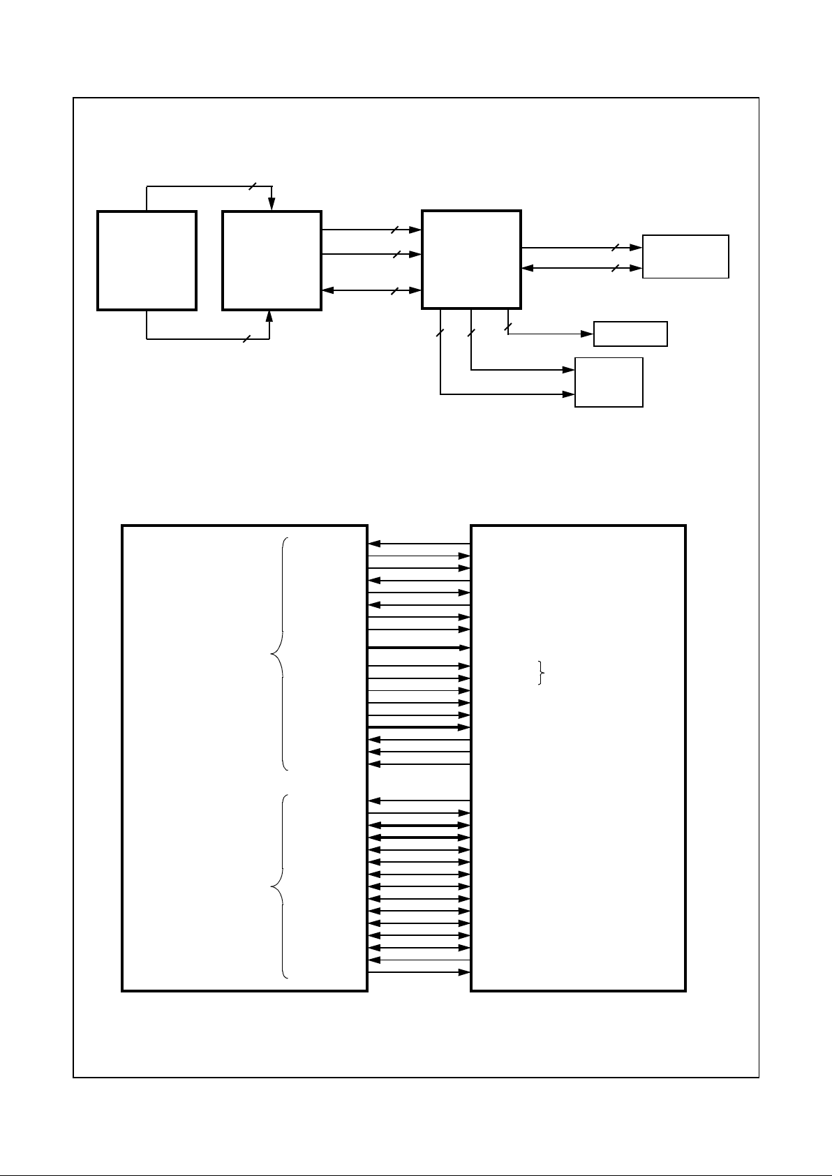
1.7 GEODE GX1/CS5530 SYSTEM DESIGNS
A GX1 processor and Geode CS5530 I/O companion
based design provides high performance using 32-bit x86
processing. The two chips integrate video, audio and memory interface functions normally performed by external
hardware.The CS5530 enables the fullfeatures of theGX1
processor with MMX support. These features include full
VGA and VESA video, 16-bit stereo sound, IDE interface,
ISA interface, SMM power management, and IBM’s AT
compatibility logic. In addition, the CS5530 provides an
Ultra DMA/33 interface, MPEG1 assist, and AC97 Version
2.0 compliant audio.
Figure 1-2 shows a basic block system diagram which also
includes the Geode CS9211 graphics companion for
designs that need to interface to a Dual Scan Super
Twisted Pneumatic (DSTN) panel (instead of a TFT panel).
Figure 1-3 shows an example of a CS9211 interface in a
typical GX1/CS5530 based system design. The CS9211
converts the digital RGB output of the CS5530 to the digital
output suitable for driving a color DSTN flat panel LCD. It
can drive all standard color DSTN flat panels up to a
1024x768 resolution.
Figures 1-4 and 1-5 show the signal connections between
the GX1 processorand the CS5530. For connections to the
CS9211, refer to the CS9211 data book.
Figure 1-2. Geode™ GX1/CS5530 System Block Diagram
YUV Port
(Video)
RGB Port
PCI Interface
SDRAM
MD[63:0]
3.3V PCI Bus
Graphics Data
Video Data
Analog RGB
Digital RGB (to TFT or DSTN Panel)
CRT
TFT
Panel
USB
(2 Ports)
AC97
Codec
Speakers
CD
ROM
Audio
Microphone
GPIO
Port
(Graphics)
Super
ISA Bus
SDRAM
Serial
Packet
Clocks
I/O
BIOS
IDE
Devices
14.31818
MHz Crystal
IDE Control
DC-DC & Battery
CS9211
Graphics
Companion
DSTN Panel
Geode™
Geode™
CS5530
I/O Companion
Geode™
GX1
Processor
Page 14
www.national.com 14 Revision 1.0
Geode™ GX1 Processor Series
Architecture Overview (Continued)
.
Figure 1-3. Geode™ CS9211 Interface System Diagram
Figure 1-4. Geode™ GX1/CS5530 Signal Connections
MemData
Addr & Control
21
16
LCD Power
3
Control
Panel Timing
424
Panel Data
DSTN/TFT
Pixel Port
18
Serial
4
PixelData
LCD
18
CS9211
Graphics
DRAM/SDRAM
256Kx16
GX1
Configuration
CS5530 I/O
Companion
Companion
Processor
Geode™
Geode™
Geode™
Video Port (YUV)
8
Timing Control
4
SYSCLK
SERIALP
IRQ13
SMI#
PCLK
CRT_HSYNC
CRT_VSYNC
PIXEL[17:0]
FP_HSYNC
FP_VSYNC
ENA_DISP
VID_VAL
VID_CLK
VID_DATA[7:0]
VID_RDY
INTR
SUSP#
SUSPA#
AD[31:0]
C/BE[3:0]#
PAR
FRAME#
IRDY#
TRDY#
STOP#
LOCK#
DEVSEL#
PERR#
SERR#
REQ0#
GX_CLK
PSERIAL
IRQ13
SMI#
PCLK
HSYNC
VSYNC
PIXEL[23:0]
FP_HSYNC
FP_VSYNC
ENA_DISP
VID_VAL
VID_CLK
VID_DATA[7:0]
VID_RDY
CPU_RST
INTR
SUSP#
SUSPA#
AD[31:0]
C/BE[3:0]#
PAR
FRAME#
IRDY#
TRDY#
STOP#
LOCK#
DEVSEL#
PERR#
SERR#
REQ#
GNT#GNT0#
Geode™ GX1 Geode™ CS5530
I/O Companion
Exclusive
Interconnect
Signals
(Do not connect to
any other device)
Nonexclusive
Interconnect
Signals
(May also connect
to other 3.3V circuitry)
Not needed if
CRT only (no TFT)
(Note)
Note: Refer to Figure 1-5 for interconnection of the pixel lines.
RESET
DCLK DCLK
Processor
Page 15
Revision 1.0 15 www.national.com
Geode™ GX1 Processor Series
Architecture Overview (Continued)
Figure 1-5. PIXEL Signal Connections
PIXEL17
PIXEL16
PIXEL15
PIXEL14
PIXEL13
PIXEL12
PIXEL11
PIXEL10
PIXEL9
PIXEL8
PIXEL7
PIXEL6
PIXEL5
PIXEL4
PIXEL3
PIXEL2
PIXEL1
Geode™ CS5530
I/O Companion
PIXEL0
PIXEL23
PIXEL22
PIXEL21
PIXEL20
PIXEL19
PIXEL18
PIXEL17
PIXEL16
PIXEL15
PIXEL14
PIXEL13
PIXEL12
PIXEL11
PIXEL10
PIXEL9
PIXEL8
PIXEL7
PIXEL6
PIXEL5
PIXEL4
PIXEL3
PIXEL2
PIXEL1
PIXEL0
R
G
B
Geode™ GX1
Processor
Page 16
www.national.com 16 Revision 1.0
Geode™ GX1 Processor Series
Architecture Overview (Continued)
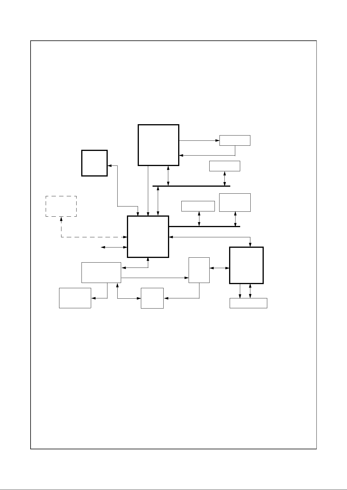
1.7.1 Reference Designs
As described previously, the GX1 series of integrated processors is designed specifically to work with National’s
Geode I/O and graphics companion devices. To help define
and drive the emerging information appliance market, several reference systems have been developed by National
Semiconductor. These GX1 processor based reference
systems provide optimized and targeted solutions for three
main segments of the information appliance market: Personal Internet Access, Thin Client, and Set-top Box. Contact your local National Semiconductor sales or field
support representative for further information on reference
designs for the information appliance market.
Figure 1-6. Example WebPAD™ System Diagram
PCMCIA
Touch
Control
512 KB DRAM
Li Batteries/
Charger
Data
3.3V PCI Bus
RF Interface
Backlight
Ultra DMA/33
Buttons
Pwr Mgmt
Embedded OS
Applications
DC Sense
Bootloader
Run-Time Diagnostics
Storage
Embedded OS
Applications
Bootloader
Run-Time Diagnostics
Storage
Microcontroller
DSTN
ISA Bus
USB Port
Control
Flash
Card
Optional
SDRAM
CS5530
I/O
Companion
Geode™
Geode™
CS9211
Graphics
Companion
Geode™
GX1
Processor
NSC
LM4549
Codec
Linear
Flash
(8 MB)
Page 17
Revision 1.0 17 www.national.com
Geode™ GX1 Processor Series
Architecture Overview (Continued)
Figure 1-7. Example Thin Client System Diagram
SDRAM SO-DIMM
Video
3.3V PCI Bus
Termination
Reset
PWR CTL
CPU Core
Power
Power
Clock
MK1491-06
TFT
USB (2x)
CRT
MIC In
Audio Out
Term ination
64 MB Flash
ISA Bus
Generator
CS5530
I/O
Companion
Geode™
Geode™
GX1
Processor
NSC
LM4546
Codec
NSC
DP83815
Ethernet
Controller
NSC
PC97317IBW/VUL
SuperI/O
Page 18
www.national.com 18 Revision 1.0
Geode™ GX1 Processor Series
Architecture Overview (Continued)
Figure 1-8. Example Set-Top Box System Diagram
CS5530
Notebook DVD
Drive
Notebook
Floppy
Drive
Internal Assembly Options
Flash
BIOS
2.5” UDMA33
Hard Drive
Headphone
Audio Line
Output
Tuner
AC3
Anlg
MIC MIC
CPU Temp.
Sensor
SDRAM DIMM
SDRAM DIMM
DMA
3.3V PCI Bus
1IN2
IN
CD In
Riser Slot
PCI Slot
Optional
LAN PCI
Card
LAN /
WAN
ISA Slot
Riser Slot
ROM Slot
WinCE ROM
Modul
e
TDA8006
LPT
COM
Mouse
(IR)
Keybd
(IR)
Front
Panel
USB
Ports
AC3
Anlg
Optional
V.90
Modem
SDRAM
PCM1723
IGS 50x5
Graphics
SAA7112
SGRAM
SGRAM
Video Port
TV Tuner
Composite
Video In
9638
TDA9851
TV
Tuner
Module
Arbiter
C-CUBE
“ZIVA”
CATV In
AC3
Digital
Tuner FM Out
VGA
S-Video
PAL or
NTSC
Audio
Line
Out
SPDIF
ISA Bus
I/O
Companion
GX1
LM4548
Codec
Processor
Geode™
Geode™
NSC
LM75
Output
FM In
Smartcard
NSC
PC97317VUL-ICF
SuperI/O
Page 19
Revision 1.0 19 www.national.com
Geode™ GX1 Processor Series
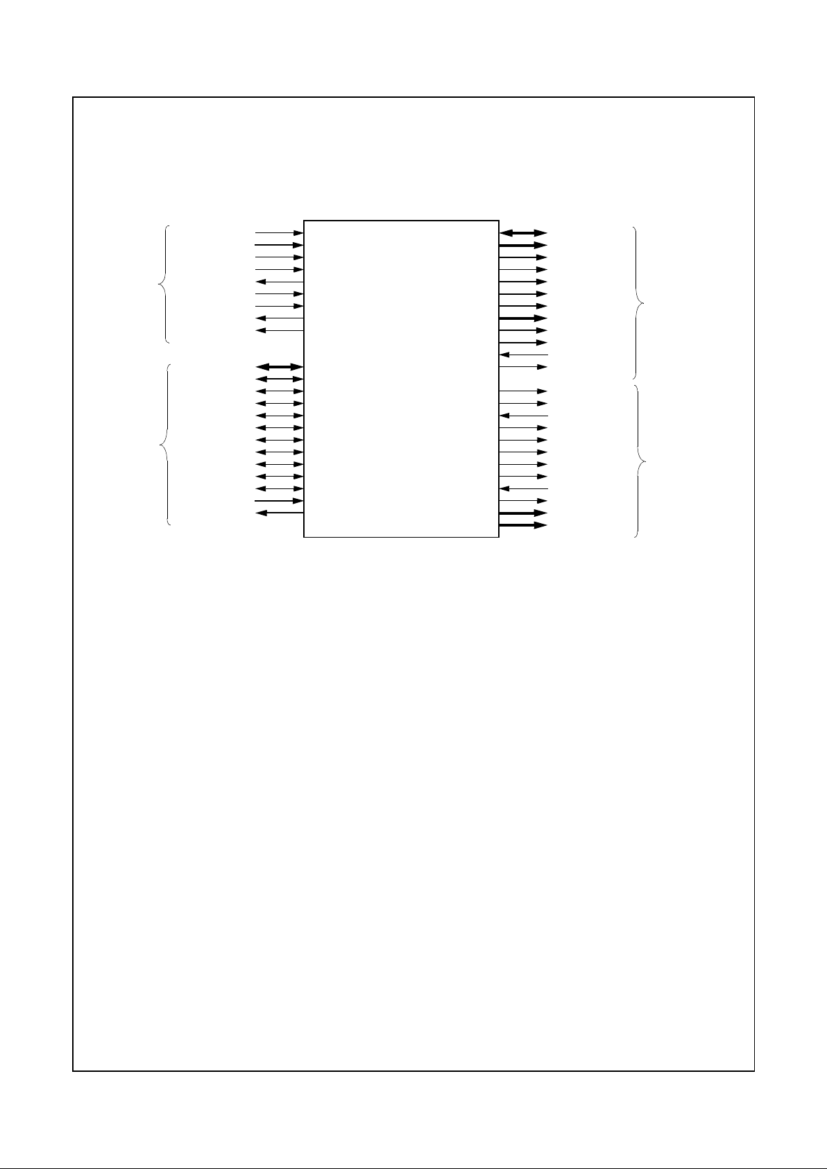
2.0 Signal Definitions
This section describes the external interface of the Geode GX1 processor. Figure 2-1 shows the signals organized by their
functional interface groups (internal test and electrical pins are not s hown).
Figure 2-1. Functional Block Di agram
SYSCLK
CLKMODE[2:0]
RESET
INTR
IRQ13
SMI#
SUSP#
SUSPA#
SERIALP
AD[31:0]
C/BE[3:0]#
PAR
FRAME#
IRDY#
TRDY#
STOP#
LOCK#
DEVSEL#
PERR#
SERR#
REQ[2:0]#
GNT[2:0]#
MD[63:0]
MA[12:0]
BA[1:0]
RASA#, RASB#
CASA#, CASB#
CS[3:0]#
WEA#, WEB#
DQM[7:0]
CKEA, CKEB
SDCLK[3:0]
SDCLK_IN
SDCLK_OUT
PCLK
VID_CLK
DCLK
CRT_HSYNC
CRT_VSYNC
FP_VSYNC
FP_HSYNC
ENA_DISP
VID_RDY
VID_VAL
VID_DATA[7:0]
PIXEL[17:0]
Memory
Controller
Interface
Video
Interface
Signals
PCI
Interface
Signals
System
Interface
Signals
Signals
GX1
Processor
Geode™
Page 20
www.national.com 20 Revision 1.0
Geode™ GX1 Processor Series
Signal Definitions (Continued)
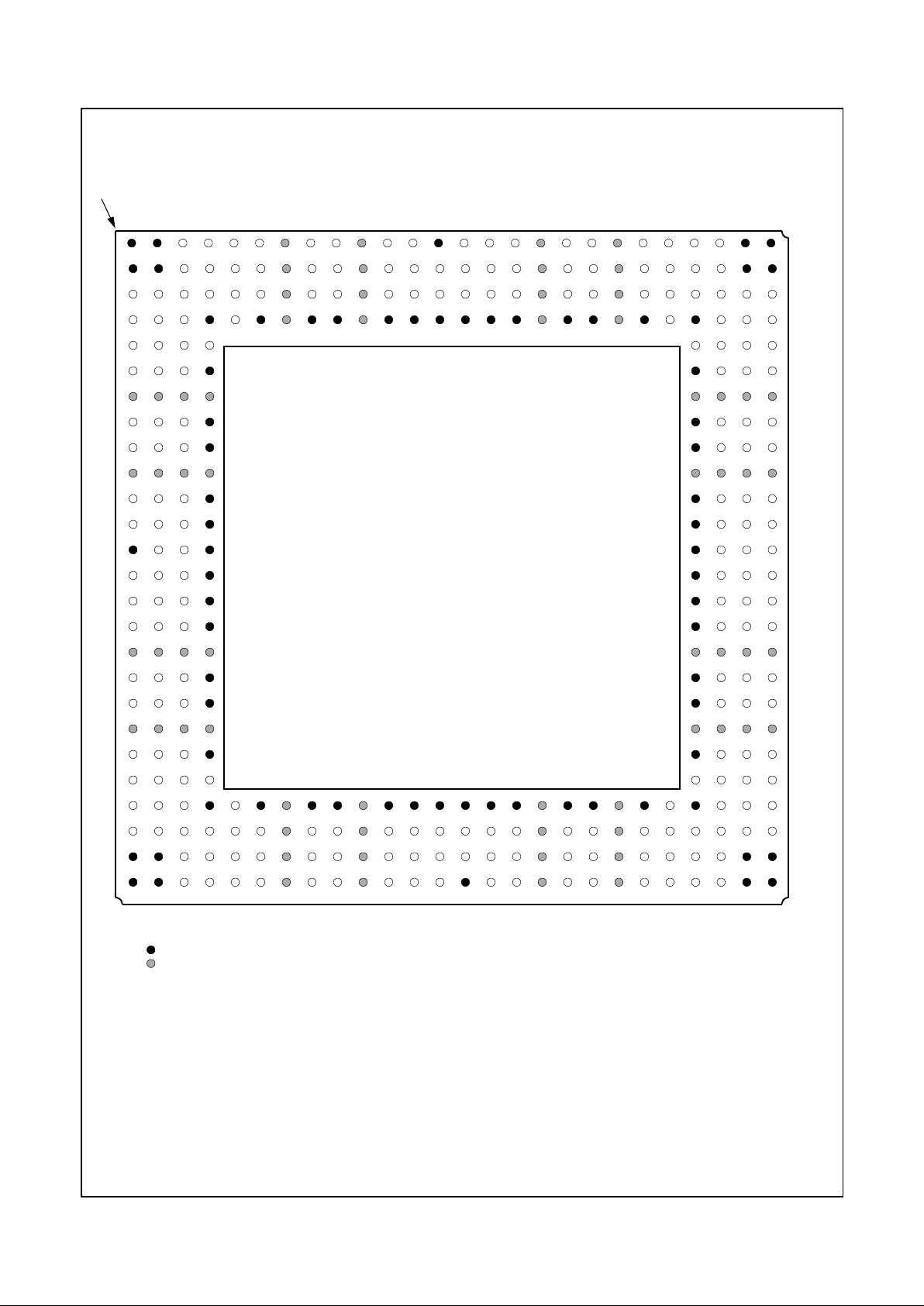
2.1 PIN ASSIGNMENTS
The tables in this section use several common abbreviations. Table 2-1 lists the mnemonics and their meanings.
Figure 2-2 shows the pin assignment for the 352 BGA with
Table 2-2 and Table 2-3 listing the pin assignments sorted
by pin number and alphabetically by signal name, respectively.
Figure 2-3 shows the pin assignment for the 320 SPGA
with Table 2-4 and Table 2-5 listing the pin assignments
sorted by pin number and alphabetically by signal name,
respectively.
In Section 2.2 “Signal Descriptions” on page 31 a description of each signal is provided within its associated functional group.
Table 2-1. Pin Type Definitions
Mnemonic Definition
I Standard input pin.
I/O Bidirectional pin.
O Totem-pole output.
OD Open-drain output structure that
allows multiple devices to share the
pin in a wired-OR configuration.
PU Pull-up resistor.
PD Pull-down resistor.
s/t/s Sustained tri-state, an active-low tri-
state signal ownedand drivenby one
and only one agent at a time. The
agent that drives an s/t/s pin low
must drive it high for at least one
clock before letting it float. A new
agent cannot start dr iving an s/t/s
signal any sooner than one clock
after the previous owner lets it float.
Apull-up resistor on the motherboard
is required to sustain the inactive
state until another agent drives it.
VCC (PWR) Power pin.
VSS (GND) Ground pin.
# The "#" symbol at the end of a signal
name indicates that the active, or
asserted state occurs when the sig-
nal is at a low voltage level.When "#"
is not present after the signal name,
the signal is asserted whenat a high
voltage level.
t/s Tri-state signal.
Page 21
Revision 1.0 21 www.national.co
Geode™ GX1 Processor Series
Signal Definitions (Continued)
Figure 2-2. 352 BGA Pin Assignment Diagram
(
For order information, refer to Section A.1 “Order Information” on page 246.)
1234567891011121314151617181920
21 22 23 24 25 26
A
B
C
D
E
F
G
H
J
K
L
M
N
P
R
T
U
V
W
Y
AA
AB
AC
AD
AE
AF
Index Corner
VSS VSS AD27 AD24 AD21 AD16 VCC2 FRAM# DEVS# VCC3 PERR# AD15 VSS AD11 CBE0# AD6 VCC2 AD4 AD2 VCC3 AD0 AD1 TEST2 MD2 VSS VSS
VSS VSS AD28 AD25 AD22 AD18 VCC2 CBE2# TRDY# VCC3 LOCK# PAR AD14 AD12 AD9 AD7 VCC2 INTR AD3 VCC3 TEST1 TEST3 MD1 MD33 VSS VSS
AD29 AD31 AD30 AD26 AD23 AD19 VCC2 AD17 IRDY# VCC3 STOP# SERR# CBE1# AD13 AD10 AD8 VCC2 AD5 SMI# VCC3 TEST0 IRQ13 MD32 MD34 MD3 MD35
GNT0# TDI REQ2# VSS CBE3# VSS VCC2 VSS VSS VCC3 VSS VSS VSS VSS VSS VSS VCC2 VSS VSS VCC3 VSS MD0 VSS MD4 MD36 TDN
GNT2#SUSPA#REQ0# AD20 MD6 TDP MD5 MD37
TD0 GNT1# TEST VSS VSS MD38 MD7 MD39
VCC3 VCC3 VCC3 VCC3 VCC3 VCC3 VCC3 VCC3
TMS SUSP# REQ1# VSS VSS MD8 MD40 M D9
FPVSY TCLK RESET VSS VSS MD41 MD10 MD42
VCC2 VCC2 VCC2 VCC2 VCC2 VCC2 VCC2 VCC2
CKM1 FPHSY SERLP VSS VSS MD11 MD43 MD12
CKM2 VIDVAL CKM0 VSS VSS MD44 MD13 MD45
VSS PIX1 PIX0 VSS VSS MD14 MD46 MD15
VIDCLK PIX3 PIX2 VSS VSS MD47 CASA# SYSCLK
PIX4 PIX5 PIX6 VSS VSS WEB# WEA# CASB#
PIX7 PIX8 PIX9 VSS VSS DQM0 DQM4 DQM1
VCC3 VCC3 VCC3 VCC3 VCC3 VCC3 VCC3 VCC3
PIX10 PIX11 PIX12 VSS VSS DQM5 CS2# CS0#
PIX13 CRTHSY PIX14 VSS VSS RASA# RASB# MA0
VCC2 VCC2 VCC2 VCC2 VCC2 VCC2 VCC2 VCC2
PIX15 PIX16 CRTVSY VSS VSS MA1 MA2 MA3
DCLK PIX17 VDAT6 VDAT7 MA4 MA5 MA6 MA7
PCLK FLT# VDAT4 VSS NC VSS VCC2 VSS VSS VCC3 VSS VSS VSS VSS VSS VSS VCC2 VSS VSS VCC3 VSS DQM6 VSS MA8 MA9 MA10
VRDY VDAT5 VDAT3 VDAT0 EDISP MD63 VCC2 MD62 MD 29 VCC3 MD59 MD26 MD56 MD55 MD22 CKEB VCC2 MD51 MD18 VCC3 MD48 DQM3 CS1# MA11 BA0 BA1
VSS VSSVDAT2SCLK3SCLK1RWCLKVCC2SCKINMD61VCC3MD28MD58MD25MD24MD54MD21VCC2MD20MD50VCC3MD17DQM7CS3#MA12 VSS VSS
VSS VSS VDAT1 SCLK0 SCLK2 MD31 VCC2 SCKOUT MD30 VCC3 MD60 MD27 MD57 VSS MD23 MD53 VCC2 MD52 MD19 VCC3 MD49 MD16 DQM2 CKEA VSS VSS
1234567891011121314151617181920
21 22 23 24 25 26
A
B
C
D
E
F
G
H
J
K
L
M
N
P
R
T
U
V
W
Y
AA
AB
AC
AD
AE
AF
352 BGA - Top View
Note: Signal names have been abbreviated in this f ig ure due to space constraints.
= GND terminal
= PWR terminal (VCC2 = VCC_CORE; VCC3 = VCC_IO)
GX1
Processor
Geode™
Page 22

www.national.com 22 Revision 1.0
Geode™ GX1 Processor Series
Signal Definitions (Continued)
Table 2-2. 352 BGA Pin Assignments - Sorted by Pin Number
Pin
No. Signal Name
A1 VSS
A2 VSS
A3 AD27
A4 AD24
A5 AD21
A6 AD16
A7 VCC2
A8 FRAME#
A9 DEVSEL#
A10 VCC3
A11 PERR#
A12 AD15
A13 VSS
A14 AD11
A15 C/BE0#
A16 AD6
A17 VCC2
A18 AD4
A19 AD2
A20 VCC3
A21 AD0
A22 AD1
A23 TEST2
A24 MD2
A25 VSS
A26 VSS
B1 VSS
B2 VSS
B3 AD28
B4 AD25
B5 AD22
B6 AD18
B7 VCC2
B8 C/BE2#
B9 TRDY#
B10 VCC3
B11 LOCK#
B12 PAR
B13 AD14
B14 AD12
B15 AD9
B16 AD7
B17 VCC2
B18 INTR
B19 AD3
B20 VCC3
B21 TEST1
B22 TEST3
B23 MD1
B24 MD33
B25 VSS
B26 VSS
C1 AD29
C2 AD31
C3 AD30
C4 AD26
C5 AD23
C6 AD19
C7 VCC2
C8 AD17
C9 IRDY#
C10 VCC3
C11 STOP#
C12 SERR#
C13 C/BE1#
C14 AD13
C15 AD10
C16 AD8
C17 VCC2
C18 AD5
C19 SMI#
C20 VCC3
C21 TEST0
C22 IRQ13
C23 MD32
C24 MD34
C25 MD3
C26 MD35
D1 GNT0#
D2 TDI
D3 REQ2#
D4 VSS
D5 C/BE3#
D6 VSS
D7 VCC2
D8 VSS
D9 VSS
D10 VCC3
D11 VSS
D12 VSS
D13 VSS
D14 VSS
D15 VSS
D16 VSS
D17 VCC2
D18 VSS
Pin
No. Signal Name
D19 VSS
D20 VCC3
D21 VSS
D22 MD0
D23 VSS
D24 MD4
D25 MD36
D26 TDN
E1 GNT2#
E2 SUSPA#
E3 REQ0#
E4 AD20
E23 MD6
E24 TDP
E25 MD5
E26 MD37
F1 TDO
F2 GNT1#
F3 TEST
F4 VSS
F23 VSS
F24 MD38
F25 MD7
F26 MD39
G1 VCC3
G2 VCC3
G3 VCC3
G4 VCC3
G23 VCC3
G24 VCC3
G25 VCC3
G26 VCC3
H1 TMS
H2 SUSP#
H3 REQ1#
H4 VSS
H23 VSS
H24 MD8
H25 MD40
H26 MD9
J1 FP_VSYNC
J2 TCLK
J3 RESET
J4 VSS
J23 VSS
J24 MD41
J25 MD10
J26 MD42
Pin
No. Signal Name
K1 VCC2
K2 VCC2
K3 VCC2
K4 VCC2
K23 VCC2
K24 VCC2
K25 VCC2
K26 VCC2
L1 CLKMODE1
L2 FP_HSYNC
L3 SERIALP
L4 VSS
L23 VSS
L24 MD11
L25 MD43
L26 MD12
M1 CLKMODE2
M2 VID_VAL
M3 CLKMODE0
M4 VSS
M23 VSS
M24 MD44
M25 MD13
M26 MD45
N1 VSS
N2 PIXEL1
N3 PIXEL0
N4 VSS
N23 VSS
N24 MD14
N25 MD46
N26 MD15
P1 VID_CLK
P2 PIXEL3
P3 PIXEL2
P4 VSS
P23 VSS
P24 MD47
P25 CASA#
P26 SYSCLK
R1 PIXEL4
R2 PIXEL5
R3 PIXEL6
R4 VSS
R23 VSS
R24 WEB#
R25 WEA#
R26 CASB#
Pin
No. Signal Name
T1 PIXEL7
T2 PIXEL8
T3 PIXEL9
T4 VSS
T23 VSS
T24 DQM0
T25 DQM4
T26 DQM1
U1 VCC3
U2 VCC3
U3 VCC3
U4 VCC3
U23 VCC3
U24 VCC3
U25 VCC3
U26 VCC3
V1 PIXEL10
V2 PIXEL11
V3 PIXEL12
V4 VSS
V23 VSS
V24 DQM5
V25 CS2#
V26 CS0#
W1 PIXEL13
W2 CRT_HSYNC
W3 PIXEL14
W4 VSS
W23 VSS
W24 RASA#
W25 RASB#
W26 MA0
Y1 VCC2
Y2 VCC2
Y3 VCC2
Y4 VCC2
Y23 VCC2
Y24 VCC2
Y25 VCC2
Y26 VCC2
AA1 PIXEL15
AA2 PIXEL16
AA3 CRT_VSYNC
AA4 VSS
AA23 VSS
AA24 MA1
AA25 MA2
AA26 MA3
Pin
No. Signal Name
Page 23
Revision 1.0 23 www.national.co
Geode™ GX1 Processor Series
Signal Definitions (Continued)
AB1 DCLK
AB2 PI XEL17
AB3 VID_DATA6
AB4 VID_DATA7
AB23 MA4
AB24 MA5
AB25 MA6
AB26 MA7
AC1 PCLK
AC2 FLT#
AC3 VID_DATA4
AC4 VSS
AC5 NC
AC6 VSS
AC7 VCC2
AC8 VSS
AC9 VSS
AC10 VCC3
AC11 VSS
AC12 VSS
AC13 VSS
AC14 VSS
AC15 VSS
Pin
No. Signal Name
AC16 VSS
AC17 VCC2
AC18 VSS
AC19 VSS
AC20 VCC3
AC21 VSS
AC22 DQM6
AC23 VSS
AC24 MA8
AC25 MA9
AC26 MA10
AD1 VID_RDY
AD2 VID_DATA5
AD3 VID_DATA3
AD4 VID_DATA0
AD5 ENA_DISP
AD6 MD63
AD7 VCC2
AD8 MD62
AD9 MD29
AD10 VCC3
AD11 MD59
AD12 MD26
Pin
No. Signal Name
AD13 MD56
AD14 MD55
AD15 MD22
AD16 CKEB
AD17 VCC2
AD18 MD51
AD19 MD18
AD20 VCC3
AD21 MD48
AD22 DQM3
AD23 CS1#
AD24 MA11
AD25 BA0
AD26 BA1
AE1 VSS
AE2 VSS
AE3 VID_DATA2
AE4 SDCLK3
AE5 SDCLK1
AE6 RW_CLK
AE7 VCC2
AE8 SDCLK_IN
AE9 MD61
Pin
No. Signal Name
AE10 VCC3
AE11 MD28
AE12 MD58
AE13 MD25
AE14 MD24
AE15 MD54
AE16 MD21
AE17 VCC2
AE18 MD20
AE19 MD50
AE20 VCC3
AE21 MD17
AE22 DQM7
AE23 CS3#
AE24 MA12
AE25 VSS
AE26 VSS
AF1 VSS
AF2 VSS
AF3 VID_DATA1
AF4 SDCLK0
AF5 SDCLK2
AF6 MD31
Pin
No. Signal Name
AF7 VCC2
AF8 SDCLK_OUT
AF9 MD30
AF10 VCC3
AF11 MD60
AF12 MD27
AF13 MD57
AF14 VSS
AF15 MD23
AF16 MD53
AF17 VCC2
AF18 MD52
AF19 MD19
AF20 VCC3
AF21 MD49
AF22 MD16
AF23 DQM2
AF24 CKEA
AF25 VSS
AF26 VSS
Pin
No. Signal Name
Table 2-2. 352 BGA Pin Assignments - Sorted by Pin Number (Continued)
Page 24

www.national.com 24 Revision 1.0
Geode™ GX1 Processor Series
Signal Definitions (Continued)
Table 2-3. 352 BGA Pin Assignments - Sorted Alphabetically by Signal Name
Signal Name Type Pin No.
1
AD0 I/O A21
AD1 I/O A22
AD2 I/O A19
AD3 I/O B19
AD4 I/O A18
AD5 I/O C18
AD6 I/O A16
AD7 I/O B16
AD8 I/O C16
AD9 I/O B15
AD10 I/O C15
AD11 I/O A14
AD12 I/O B14
AD13 I/O C14
AD14 I/O B13
AD15 I/O A12
AD16 I/O A6
AD17 I/O C8
AD18 I/O B6
AD19 I/O C6
AD20 I/O E4
AD21 I/O A5
AD22 I/O B5
AD23 I/O C5
AD24 I/O A4
AD25 I/O B4
AD26 I/O C4
AD27 I/O A3
AD28 I/O B3
AD29 I/O C1
AD30 I/O C3
AD31 I/O C2
BA0 O AD25
BA1 O AD26
CASA# O P25
CASB# O R26
C/BE0# I/O A15
C/BE1# I/O C13
C/BE2# I/O B8
C/BE3# I/O D5
CKEA O AF24
CKEB O AD16
CLKMODE0 I M3
CLKMODE1 I L1
CLKMODE2 I M1
CRT_HSYNC O W2
CRT_VSYNC O AA3
CS0# O V26
CS1# O AD23
CS2# O V25
CS3# O AE23
DCLK I AB1
DEVSEL# s/t/s A9 (PU)
DQM0 O T24
DQM1 O T26
DQM2 O AF23
DQM3 O AD22
DQM4 O T25
DQM5 O V24
DQM6 O AC22
DQM7 O AE22
ENA_DISP O AD5
FLT# I AC2
FP_HSYNC O L2
FP_VSYNC O J1
FRAME# s/t/s A8 (PU)
GNT0# O D1
GNT1# O F2
GNT2# O E1
INTR I B18
IRDY# s/t/s C9 (PU)
IRQ13 O C22
LOCK# s/t/s B11 (PU)
MA0 O W26
MA1 O AA24
MA2 O AA25
MA3 O AA26
MA4 O AB23
MA5 O AB24
MA6 O AB25
MA7 O AB26
MA8 O AC24
MA9 O AC25
MA10 O AC26
MA11 O AD24
MA12 O AE24
MD0 I/O D22
MD1 I/O B23
MD2 I/O A24
MD3 I/O C25
MD4 I/O D24
MD5 I/O E25
MD6 I/O E23
MD7 I/O F25
MD8 I/O H24
MD9 I/O H26
MD10 I/O J25
MD11 I/O L24
MD12 I/O L26
MD13 I/O M25
MD14 I/O N24
MD15 I/O N26
MD16 I/O AF22
MD17 I/O AE21
MD18 I/O AD19
MD19 I/O AF19
Signal Name Type Pin No.
1
MD20 I/O AE18
MD21 I/O AE16
MD22 I/O AD15
MD23 I/O AF15
MD24 I/O AE14
MD25 I/O AE13
MD26 I/O AD12
MD27 I/O AF12
MD28 I/O AE11
MD29 I/O AD9
MD30 I/O AF9
MD31 I/O AF6
MD32 I/O C23
MD33 I/O B24
MD34 I/O C24
MD35 I/O C26
MD36 I/O D25
MD37 I/O E26
MD38 I/O F24
MD39 I/O F26
MD40 I/O H25
MD41 I/O J24
MD42 I/O J26
MD43 I/O L25
MD44 I/O M24
MD45 I/O M26
MD46 I/O N25
MD47 I/O P24
MD48 I/O AD21
MD49 I/O AF21
MD50 I/O AE19
MD51 I/O AD18
MD52 I/O AF18
MD53 I/O AF16
MD54 I/O AE15
MD55 I/O AD14
MD56 I/O AD13
MD57 I/O AF13
MD58 I/O AE12
MD59 I/O AD11
MD60 I/O AF11
MD61 I/O AE9
MD62 I/O AD8
MD63 I/O AD6
NC -- AC5
PAR I/O B12
PCLK O AC1
PERR# s/t/s A11 (PU)
PIXEL0 O N3
PIXEL1 O N2
PIXEL2 O P3
PIXEL3 O P2
PIXEL4 O R1
Signal Name Type Pin No.
1
PIXEL5 O R2
PIXEL6 O R3
PIXEL7 O T1
PIXEL8 O T2
PIXEL9 O T3
PIXEL10 O V1
PIXEL11 O V2
PIXEL12 O V3
PIXEL13 O W1
PIXEL14 O W3
PIXEL15 O AA1
PIXEL16 O AA2
PIXEL17 O AB2
RASA# O W24
RASB# O W25
REQ0# I E3 (PU)
REQ1# I H3 (PU)
REQ2# I D3 (PU)
RESET I J3
RW_CLK O AE6
SDCLK_IN I AE8
SDCLK_OUT O AF8
SDCLK0 O AF4
SDCLK1 O AE5
SDCLK2 O AF5
SDCLK3 O AE4
SERIALP O L3
SERR# OD C12 (PU)
SMI# I C19
STOP# s/t/s C11 (PU)
SUSP# I H2 (PU)
SUSPA# O E2
SYSCLK I P2 6
TCLK I J2 (PU)
TDI I D2 (PU)
TDN O D26
TDO O F1
TDP O E24
TEST I F3 (PD)
TEST0 O C21
TEST1 O B21
TEST2 O A23
TEST3 O B22
TMS I H1 (PU)
TRDY# s/t/s B9 (PU)
VCC2 PWR A7
VCC2 PWR A17
VCC2 PWR B7
VCC2 PWR B17
VCC2 PWR C7
VCC2 PWR C17
VCC2 PWR D7
VCC2 PWR D17
Signal Name Type Pin No.
1
Page 25
Revision 1.0 25 www.national.co
Geode™ GX1 Processor Series
Signal Definitions (Continued)
VCC2 PWR K1
VCC2 PWR K2
VCC2 PWR K3
VCC2 PWR K4
VCC2 PWR K23
VCC2 PWR K24
VCC2 PWR K25
VCC2 PWR K26
VCC2 PWR Y1
VCC2 PWR Y2
VCC2 PWR Y3
VCC2 PWR Y4
VCC2 PWR Y23
VCC2 PWR Y24
VCC2 PWR Y25
VCC2 PWR Y26
VCC2 PWR AC7
VCC2 PWR AC17
VCC2 PWR AD7
VCC2 PWR AD17
VCC2 PWR AE7
VCC2 PWR AE17
VCC2 PWR AF7
VCC2 PWR AF17
VCC3 PWR A10
VCC3 PWR A20
VCC3 PWR B10
VCC3 PWR B20
VCC3 PWR C10
VCC3 PWR C20
VCC3 PWR D10
VCC3 PWR D20
VCC3 PWR G1
VCC3 PWR G2
VCC3 PWR G3
VCC3 PWR G4
VCC3 PWR G23
Signal Name Type Pin No.
1
VCC3 PWR G24
VCC3 PWR G25
VCC3 PWR G26
VCC3 PWR U1
VCC3 PWR U2
VCC3 PWR U3
VCC3 PWR U4
VCC3 PWR U23
VCC3 PWR U24
VCC3 PWR U25
VCC3 PWR U26
VCC3 PWR AC10
VCC3 PWR AC20
VCC3 PWR AD10
VCC3 PWR AD20
VCC3 PWR AE10
VCC3 PWR AE20
VCC3 PWR AF10
VCC3 PWR AF20
VID_CLK O P1
VID_DATA0 O AD4
VID_DATA1 O AF3
VID_DATA2 O AE3
VID_DATA3 O AD3
VID_DATA4 O AC3
VID_DATA5 O AD2
VID_DATA6 O AB3
VID_DATA7 O AB4
VID_RDY I AD1
VID_VAL O M2
VSS GND A1
VSS GND A2
VSS GND A13
VSS GND A25
VSS GND A26
VSS GND B1
VSS GND B2
Signal Name Type Pin No.
1
VSS GND B25
VSS GND B26
VSS GND D4
VSS GND D6
VSS GND D8
VSS GND D9
VSS GND D11
VSS GND D12
VSS GND D13
VSS GND D14
VSS GND D15
VSS GND D16
VSS GND D18
VSS GND D19
VSS GND D21
VSS GND D23
VSS GND F4
VSS GND F23
VSS GND H4
VSS GND H23
VSS GND J4
VSS GND J23
VSS GND L4
VSS GND L23
VSS GND M4
VSS GND M23
VSS GND N1
VSS GND N4
VSS GND N23
VSS GND P4
VSS GND P23
VSS GND R4
VSS GND R23
VSS GND T4
VSS GND T23
VSS GND V4
VSS GND V23
Signal Name Type Pin No.
1
VSS GND W4
VSS GND W23
VSS GND AA4
VSS GND AA23
VSS GND AC4
VSS GND AC6
VSS GND AC8
VSS GND AC9
VSS GND AC11
VSS GND AC12
VSS GND AC13
VSS GND AC14
VSS GND AC15
VSS GND AC16
VSS GND AC18
VSS GND AC19
VSS GND AC21
VSS GND AC23
VSS GND AE1
VSS GND AE2
VSS GND AE25
VSS GND AE26
VSS GND AF1
VSS GND AF2
VSS GND AF14
VSS GND AF25
VSS GND AF26
WEA# O R25
WEB# O R24
1. PU/PD indicates pin is internally connected to a
weak (> 20-kohm) pull-up/down resistor.
Signal Name Type Pin No.
1
Table 2-3. 352 BGA Pin Assignments - Sorted Alphabetically by Signal Name (Continued)
Page 26
www.national.com 26 Revision 1.0
Geode™ GX1 Processor Series
Signal Definitions (Continued)
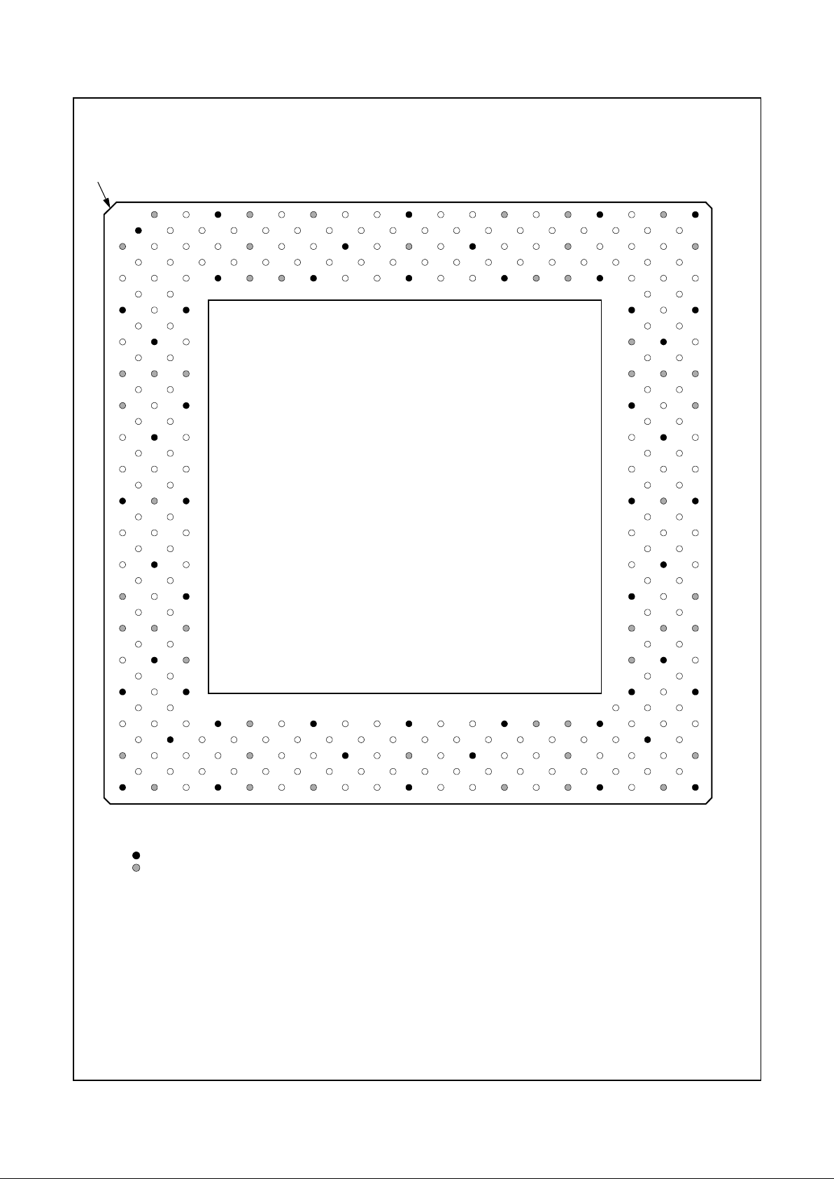
Figure 2-3. 320 SPGA Pin As signment Diagram
(For order information, refer to Section A.1 “Order Information” on page 246.)
1234567891011121314151617181920
21 22 23 24 25 26
A
B
C
D
E
F
G
H
J
K
L
M
N
P
Q
R
S
T
U
V
AA
AB
AC
AD
AE
AF
Index Corner
27 28 29 30 31 32 33 34 35 36 37
AG
AH
AJ
AK
AL
AM
W
Y
X
Z
AN
A
B
C
D
E
F
G
H
J
K
L
M
N
P
Q
R
S
T
U
V
AA
AB
AC
AD
AE
AF
AG
AH
AJ
AK
AL
AM
W
Y
X
Z
AN
1234567891011121314151617181920
21 22 23 24 25 26 27 28 29 30 31 32 33 34 35 36 37
VCC3 AD25 VSS VCC2 AD16 VCC3 STOP# SERR# VSS AD11 AD8 VCC3 AD2 VCC2 VSS TEST0 VCC3 VSS
VSS AD27 CBE3# AD21 AD19 CBE2# TRDY# LOCK# CBE1# AD13 AD9 AD6 AD3 SMI# AD1 TEST2 MD33 MD2
VCC3 AD31 AD26 AD23 VCC2 AD18 FRAME# VSS PAR VCC3 AD10 VSS AD4 AD0 VCC2 IRQ13 MD1 MD34 VCC3
AD30 AD29 AD24 AD22 AD20 AD17 IRDY# PERR# AD14 AD12 AD7 INTR TEST1 TEST3 MD0 MD32 MD3 MD35
REQ0# REQ2# AD28 VSS VCC2 VCC2 VSS DEVSEL# AD15 VSS CBE0# AD5 VSS VCC2 VCC2 VSS MD4 MD36 TDN
GNT0# TDI MD5 TDP
VSS CKMD2 VSS VSS MD37 VSS
GNT2# SUSPA#
TDO VSS TEST
REQ1# GNT1#
VCC2 VCC2 VCC2
RESET SUSP#
VCC3 TMS VSS
FPVSYNC TCLK
SERIALP VSS NC
CKMD1 FPHSYNC
CKMD0 VID_VAL PIX0
PIX1 PIX2
VSS VCC3 VSS
PIX3 VID_CLK
PIX6 PIX5 PIX4
NC PIX9
PIX8 VSS PIX7
NC PIX10
VCC3 PIX11 VSS
PIX12 PIX13
VCC2 VCC2 VCC2
CRTHSYNC DCLK
PIX14 VSS VCC2
PIX15 PIX16
VSS PIX17 VSS
CRTVSYNC VDAT6
MD6 MD38
VCC2 VSS MD7
MD39 MD8
VCC2 VCC2 VCC2
MD40 MD9
VSS MD41 VCC3
MD10 MD42
MD11 VSS MD43
MD44 MD12
MD14 MD13 MD45
MD15 MD46
VSS VCC3 VSS
SYSCLK MD47
WEA# W EB# CASA#
DQM0 CASB#
DQM1 VSS DQM4
CS2# DQM5
VSS CS0# VCC3
RASB# RASA#
VCC2 VCC2 VCC2
VCC2 VSS MA1
MA2 MA0
MA4 MA3
VSS MA5 VSS
MA8 MA6MA10
PCLK FLT# VDAT5 VSS VCC2 MD31 VSS MD60 MD57 VSS MD22 MD52 VSS VCC2 VCC2 VSS BA1 MA9 MA7
VRDY VS S VDAT0 S DCLK0 SDCLK2 SDCLKIN MD29 MD27 MD56 MD55 MD21 MD20 MD50 MD16 DQ M3 CS3#
VSS BA0
VCC2 VDAT4 VDAT2 SDCLK1 VCC2 RWCLK SDCLKOUT VSS MD58 VCC3 MD23 VSS MD19 MD49 VCC2 DQM6 CKEA MA11 VCC3
VDAT7 VDAT3 ENDIS SDCLK3 MD63 MD30 MD61 MD59 MD25 MD24 MD53 MD51 MD18 MD48 DQM7 DQM2 MA12 NC
VSS VCC2 VDAT1 VSS VCC2 MD62 VCC3 MD28 MD26 VSS MD54 CKEB VCC3 MD17 VCC2 VSS CS1# VCC3 VSS
Note: Signal names have been abbreviated in this f ig ure due to space constraints.
= Denotes GND terminal
= Denotes PWR terminal (VCC2 = VCC_CORE; VCC3 = VCC_IO)
320 SPGA - Top View
GX1
Processor
Geode™
Page 27

Revision 1.0 27 www.national.co
Geode™ GX1 Processor Series
Signal Definitions (Continued)
Table 2-4. 320 SPGA Pin Assignments - Sorted by Pin Number
Pin
No. Signal Name
A3 VCC3
A5 AD25
A7 VSS
A9 VCC2
A11 AD16
A13 VCC3
A15 STOP#
A17 SERR#
A19 VSS
A21 AD11
A23 AD8
A25 VCC3
A27 AD2
A29 VCC2
A31 VSS
A33 TEST0
A35 VCC3
A37 VSS
B2 VSS
B4 AD27
B6 C/BE3#
B8 AD21
B10 AD19
B12 C/BE2#
B14 TRDY#
B16 LOCK#
B18 C/BE1#
B20 AD13
B22 AD9
B24 AD6
B26 AD3
B28 SMI#
B30 AD1
B32 TEST2
B34 MD33
B36 MD2
C1 VCC3
C3 AD31
C5 AD26
C7 AD23
C9 VCC2
C11 AD18
C13 FRAME#
C15 VSS
C17 PAR
C19 VCC3
C21 AD10
C23 VSS
C25 AD4
C27 AD0
C29 VCC2
C31 IRQ13
C33 MD1
C35 MD34
C37 VCC3
D2 AD30
D4 AD29
D6 AD24
D8 AD22
D10 AD20
D12 AD17
D14 IRDY#
D16 PERR#
D18 AD14
D20 AD12
D22 AD7
D24 INTR
D26 TEST1
D28 TEST3
D30 MD0
D32 MD32
D34 MD3
D36 MD35
E1 REQ0#
E3 REQ2#
E5 AD28
E7 VSS
E9 VCC2
E11 VCC2
E13 VSS
E15 DEVSEL#
E17 AD15
E19 VSS
E21 C/BE0#
E23 AD5
E25 VSS
E27 VCC2
E29 VCC2
E31 VSS
E33 MD4
E35 MD36
E37 TDN
F2 GNT0#
F4 TDI
F34 MD5
F36 TDP
Pin
No. Signal Name
G1 VSS
G3 CLKMODE2
G5 VSS
G33 VSS
G35 MD37
G37 VSS
H2 GNT2#
H4 SUSPA#
H34 MD6
H36 MD38
J1 TDO
J3 VSS
J5 TEST
J33 VCC2
J35 VSS
J37 MD7
K2 REQ1#
K4 GNT1#
K34 MD39
K36 MD8
L1 VCC2
L3 VCC2
L5 VCC2
L33 VCC2
L35 VCC2
L37 VCC2
M2 RESET
M4 SUSP#
M34 MD40
M36 MD9
N1 VCC3
N3 TMS
N5 VSS
N33 VSS
N35 MD41
N37 VCC3
P2 FP_VSYNC
P4 TCLK
P34 MD10
P36 MD42
Q1 SERIALP
Q3 VSS
Q5 NC
Q33 MD11
Q35 VSS
Q37 MD43
R2 CLKMODE1
R4 FP_HSYNC
Pin
No. Signal Name
R34 MD44
R36 MD12
S1 CLKMODE0
S3 VID_VAL
S5 PIXEL0
S33 MD14
S35 MD13
S37 MD45
T2 PIXEL1
T4 PIXEL2
T34 MD15
T36 MD46
U1 VSS
U3 VCC3
U5 VSS
U33 VSS
U35 VCC3
U37 VSS
V2 PIXEL3
V4 VID_CLK
V34 SYSCLK
V36 MD47
W1 PIXEL6
W3 PIXEL5
W5 PIXEL4
W33 WEA#
W35 WEB#
W37 CASA#
X2 NC
X4 PIXEL9
X34 DQM0
X36 CASB#
Y1 PIXEL8
Y3 VSS
Y5 PIXEL7
Y33 DQM1
Y35 VSS
Y37 DQM4
Z2 NC
Z4 PIXEL10
Z34 CS2#
Z36 DQM5
AA1 VCC3
AA3 PIXEL11
AA5 VSS
AA33 VSS
AA35 CS0#
AA37 VCC3
Pin
No. Signal Nam e
AB2 PIXEL12
AB4 PIXEL13
AB34 RASB#
AB36 RASA#
AC1 VCC2
AC3 VCC2
AC5 VCC2
AC33 VCC2
AC35 VCC2
AC37 VCC2
AD2 CRT_HSYNC
AD4 DCLK
AD34 MA2
AD36 MA0
AE1 PIXEL14
AE3 VSS
AE5 VCC2
AE33 VCC2
AE35 VSS
AE37 MA1
AF2 PIXEL15
AF4 PIXEL16
AF34 MA4
AF36 MA3
AG1 VSS
AG3 PIXEL17
AG5 VSS
AG33 VSS
AG35 MA5
AG37 VSS
AH2 CRT_VSYNC
AH4 VID_DATA6
AH32 MA10
AH34 MA8
AH36 MA6
AJ1 PCLK
AJ3 FLT#
AJ5 VID_DATA5
AJ7 VSS
AJ9 VCC2
AJ11 MD31
AJ13 VSS
AJ15 MD60
AJ17 MD57
AJ19 VSS
AJ21 MD22
AJ23 MD52
AJ25 VSS
Pin
No. Signal Nam e
Page 28
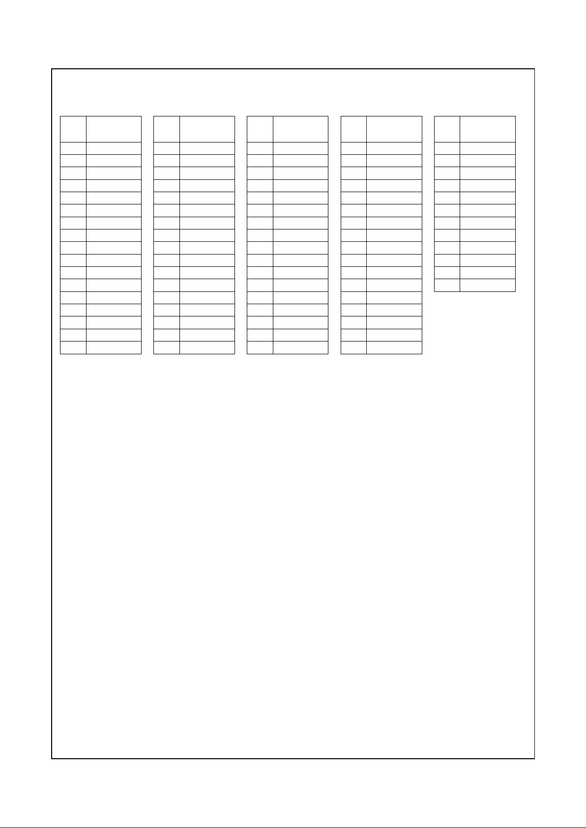
www.national.com 28 Revision 1.0
Geode™ GX1 Processor Series
Signal Definitions (Continued)
AJ27 VCC2
AJ29 VCC2
AJ31 VSS
AJ33 BA1
AJ35 MA9
AJ37 MA7
AK2 VID_RDY
AK4 VSS
AK6 VID_DATA0
AK8 SDCLK0
AK10 SDCLK2
AK12 SDCLK_IN
AK14 MD29
AK16 MD27
AK18 MD56
AK20 MD55
AK22 MD21
Pin
No. Signal Name
AK24 MD20
AK26 MD50
AK28 MD16
AK30 DQM3
AK32 CS3#
AK34 VSS
AK36 BA0
AL1 VCC2
AL3 VID_DATA4
AL5 VID_DATA2
AL7 SDCLK1
AL9 VCC2
AL11 RW_CLK
AL13 SDCLK_OUT
AL15 VSS
AL17 MD58
AL19 VCC3
Pin
No. Signal Name
AL21 MD23
AL23 VSS
AL25 MD19
AL27 MD49
AL29 VCC2
AL31 DQM6
AL33 CKEA
AL35 MA11
AL37 VCC3
AM2 VID_DATA7
AM4 VID_DATA3
AM6 ENA_DISP
AM8 SDCLK3
AM10 MD63
AM12 MD30
AM14 MD61
AM16 MD59
Pin
No. Signal Name
AM18 MD25
AM20 MD24
AM22 MD53
AM24 MD51
AM26 MD18
AM28 MD48
AM30 DQM7
AM32 DQM2
AM34 MA 12
AM36 NC
AN1 VSS
AN3 VCC2
AN5 VID_DATA1
AN7 VSS
AN9 VCC2
AN11 MD62
AN13 VCC3
Pin
No. Signal Nam e
AN15 MD28
AN17 MD26
AN19 VSS
AN21 MD54
AN23 CKEB
AN25 VCC3
AN27 MD17
AN29 VCC2
AN31 VSS
AN33 CS1#
AN35 VCC3
AN37 VSS
Pin
No. Signal Nam e
Table 2-4. 320 SPGA Pin Assignments - Sorted by Pin Number (Continued)
Page 29

Revision 1.0 29 www.national.co
Geode™ GX1 Processor Series
Signal Definitions (Continued)
Table 2-5. 320 SPGA Pin Assignments - Sorted Alphabetically by Signal Name
Signal Name Type Pin. No.
1
AD0 I/O C27
AD1 I/O B30
AD2 I/O A27
AD3 I/O B26
AD4 I/O C25
AD5 I/O E23
AD6 I/O B24
AD7 I/O D22
AD8 I/O A23
AD9 I/O B22
AD10 I/O C21
AD11 I/O A21
AD12 I/O D20
AD13 I/O B20
AD14 I/O D18
AD15 I/O E17
AD16 I/O A11
AD17 I/O D12
AD18 I/O C11
AD19 I/O B10
AD20 I/O D10
AD21 I/O B8
AD22 I/O D8
AD23 I/O C7
AD24 I/O D6
AD25 I/O A5
AD26 I/O C5
AD27 I/O B4
AD28 I/O E5
AD29 I/O D4
AD30 I/O D2
AD31 I/O C3
BA0 O AK36
BA1 O AJ33
CASA# O W37
CASB# O X36
C/BE0# I/O E21
C/BE1# I/O B18
C/BE2# I/O B12
C/BE3# I/O B6
CKEA O AL33
CKEB O AN23
CLKMODE0 I S1
CLKMODE1 I R2
CLKMODE2 I G3
CRT_HSYNC O AD2
CRT_VSYNC O AH2
CS0# O AA35
CS1# O AN33
CS2# O Z34
CS3# O AK32
DCLK I AD4
DEVSEL# s/t/s E15 (PU)
DQM0 O X34
DQM1 O Y33
DQM2 O AM 32
DQM3 O AK30
DQM4 O Y37
DQM5 O Z36
DQM6 O AL31
DQM7 O AM 30
ENA_DISP O AM6
FLT# I AJ3
FP_HSYNC O R4
FP_VSYNC O P2
FRAME# s/t/s C13 (PU)
GNT0# O F2
GNT1# O K4
GNT2# O H2
INTR I D24
IRDY# s/t/s D14 (PU)
IRQ13 O C31
LOCK# s/t/s B16 (PU)
MA0 O AD36
MA1 O AE37
MA2 O AD34
MA3 O AF36
MA4 O AF34
MA5 O AG35
MA6 O AH36
MA7 O AJ37
MA8 O AH34
MA9 O AJ35
MA10 O AH32
MA11 O AL35
MA12 O AM34
MD0 I/O D30
MD1 I/O C33
MD2 I/O B36
MD3 I/O D34
MD4 I/O E33
MD5 I/O F34
MD6 I/O H34
MD7 I/O J37
MD8 I/O K36
MD9 I/O M36
MD10 I/O P34
MD11 I/O Q33
MD12 I/O R36
MD13 I/O S35
MD14 I/O S33
MD15 I/O T34
MD16 I/O AK28
MD17 I/O AN27
MD18 I/O AM26
MD19 I/O AL25
Signal Name Type Pin. No.
1
MD20 I/O AK24
MD21 I/O AK22
MD22 I/O AJ21
MD23 I/O AL21
MD24 I/O AM20
MD25 I/O AM18
MD26 I/O AN17
MD27 I/O AK16
MD28 I/O AN15
MD29 I/O AK14
MD30 I/O AM12
MD31 I/O AJ11
MD32 I/O D32
MD33 I/O B34
MD34 I/O C35
MD35 I/O D36
MD36 I/O E35
MD37 I/O G35
MD38 I/O H36
MD39 I/O K34
MD40 I/O M34
MD41 I/O N35
MD42 I/O P36
MD43 I/O Q37
MD44 I/O R34
MD45 I/O S37
MD46 I/O T36
MD47 I/O V36
MD48 I/O AM28
MD49 I/O AL27
MD50 I/O AK26
MD51 I/O AM24
MD52 I/O AJ23
MD53 I/O AM22
MD54 I/O AN21
MD55 I/O AK20
MD56 I/O AK18
MD57 I/O AJ17
MD58 I/O AL17
MD59 I/O AM16
MD60 I/O AJ15
MD61 I/O AM14
MD62 I/O AN11
MD63 I/O AM10
NC -- E37
NC -- F36
NC -- Q5
NC -- X2
NC -- Z2
NC -- AM36
PAR I/O C17
PCLK O AJ1
PERR# s/t/s D16 (PU)
Signal Name Type Pin. No.
1
PIXEL0 O S5
PIXEL1 O T2
PIXEL2 O T4
PIXEL3 O V2
PIXEL4 O W5
PIXEL5 O W3
PIXEL6 O W1
PIXEL7 O Y5
PIXEL8 O Y1
PIXEL9 O X4
PIXEL10 O Z4
PIXEL11 O AA3
PIXEL12 O AB2
PIXEL13 O AB4
PIXEL14 O AE1
PIXEL15 O AF2
PIXEL16 O AF4
PIXEL17 O AG3
RASA# O AB36
RASB# O AB34
REQ0# I E1 (PU)
REQ1# I K2 (PU)
REQ2# I E3 (PU)
RESET I M2
RW_CLK O AL11
SDCLK_IN I AK12
SDCLK_OUT O AL13
SDCLK0 O AK8
SDCLK1 O AL7
SDCLK2 O AK10
SDCLK3 O AM8
SERIALP O Q1
SERR# OD A17 (PU)
SMI# I B28
STOP# s/t/s A15 (PU)
SUSP# I M4 (PU)
SUSPA# O H4
SYSCLK I V34
TCLK I P4 (PU)
TDI I F4 (PU)
TDN O E37
TDO O J1
TDP O F36
TEST I J5 (PD)
TEST0 O A33
TEST1 O D26
TEST2 O B32
TEST3 O D28
TDN O E37
TDP O F36
TMS I N3 (PU)
TRDY# s/t/s B14 (PU)
VCC2 PWR A9
Signal Name Type Pin. No.
1
Page 30
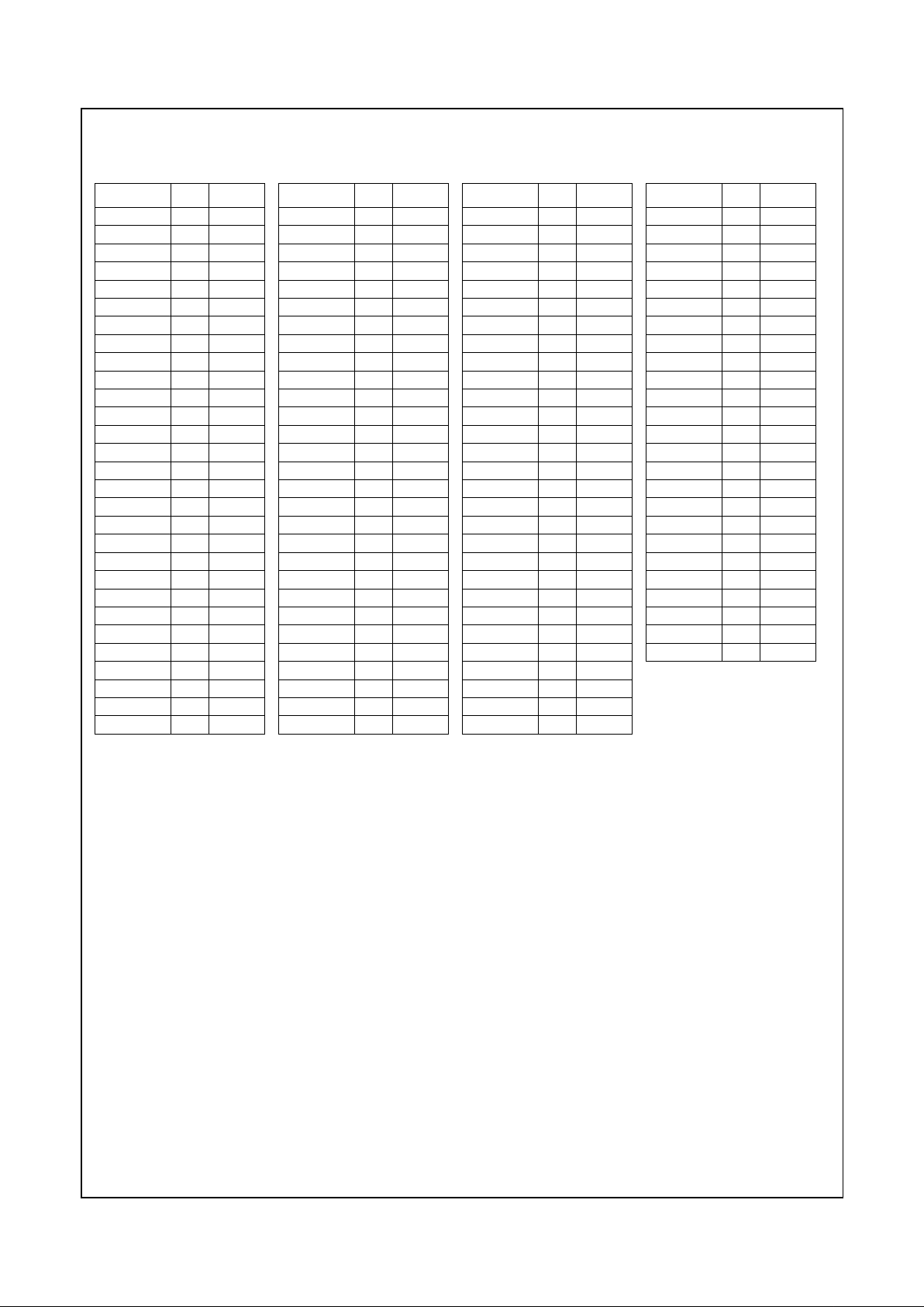
www.national.com 30 Revision 1.0
Geode™ GX1 Processor Series
Signal Definitions (Continued)
VCC2 PWR A29
VCC2 PWR C9
VCC2 PWR C29
VCC2 PWR E9
VCC2 PWR E11
VCC2 PWR E27
VCC2 PWR E29
VCC2 PWR J33
VCC2 PWR L1
VCC2 PWR L3
VCC2 PWR L5
VCC2 PWR L33
VCC2 PWR L35
VCC2 PWR L37
VCC2 PWR AC1
VCC2 PWR AC3
VCC2 PWR AC5
VCC2 PWR AC33
VCC2 PWR AC35
VCC2 PWR AC37
VCC2 PWR AE5
VCC2 PWR AE33
VCC2 PWR AJ9
VCC2 PWR AJ27
VCC2 PWR AJ29
VCC2 PWR AL1
VCC2 PWR AL9
VCC2 PWR AL29
VCC2 PWR AN3
Signal Name Type Pin. No.
1
VCC2 PWR AN9
VCC2 PWR AN29
VCC3 PWR A3
VCC3 PWR A13
VCC3 PWR A25
VCC3 PWR A35
VCC3 PWR C1
VCC3 PWR C19
VCC3 PWR C37
VCC3 PWR N1
VCC3 PWR N37
VCC3 PWR U3
VCC3 PWR U35
VCC3 PWR AA1
VCC3 PWR AA37
VCC3 PWR AL19
VCC3 PWR AL37
VCC3 PWR AN13
VCC3 PWR AN25
VCC3 PWR AN35
VID_CLK O V4
VID_DATA0 O AK6
VID_DATA1 O AN5
VID_DATA2 O AL5
VID_DATA3 O AM4
VID_DATA4 O AL3
VID_DATA5 O AJ5
VID_DATA6 O AH4
VID_DATA7 O AM2
Signal Name Type Pin. No.
1
VID_RDY I AK2
VID_VAL O S3
VSS GND A7
VSS GND A19
VSS GND A31
VSS GND A37
VSS GND B2
VSS GND C15
VSS GND C23
VSS GND E7
VSS GND E13
VSS GND E19
VSS GND E25
VSS GND E31
VSS GND G1
VSS GND G5
VSS GND G33
VSS GND G37
VSS GND J3
VSS GND J35
VSS GND N5
VSS GND N33
VSS GND Q3
VSS GND Q35
VSS GND U1
VSS GND U5
VSS GND U33
VSS GND U37
VSS GND Y3
Signal Name Type Pin. No.
1
VSS GND Y35
VSS GND AA5
VSS GND AA33
VSS GND AE3
VSS GND AE35
VSS GND AG1
VSS GND AG5
VSS GND AG33
VSS GND AG37
VSS GND AJ7
VSS GND AJ13
VSS GND AJ19
VSS GND AJ25
VSS GND AJ31
VSS GND AK4
VSS GND AK34
VSS GND AL15
VSS GND AL23
VSS GND AN1
VSS GND AN7
VSS GND AN19
VSS GND AN31
VSS GND AN37
WEA# O W33
WEB# O W35
1. PU/PD indicates pin is
internally connected to a
weak (> 20-kohm)
pull-up/down resistor.
Signal Name Type Pin. No.
1
Table 2-5. 320 SPGA Pin Assignments - Sorted Alphabetically by Signal Name (Continued)
Page 31

Revision 1.0 31 www.national.com
Geode™ GX1 Processor Series
Signal Definitions (Continued)
2.2 SIGNAL DESCRIPTIONS
2.2.1 System Interface Signals
Signal Name
BGA
Pin No.
SPGA
Pin No. Type Description
SYSCLK P26 V34 I System Clock
PCI clock is connected to SYSCLK. Theinternal clock of the GX1
processor is generated by a proprietary patentedfrequency synthesis circuit which multiplies the SYSCLK input up to ten times.
The SYSCLK to core clock multiplier is configured using the CLKMODE[2:0] inputs.
The SYSCLK input is a fixed frequencywhich can only be stopped
or varied when the GX1 processor is in full 3V Suspend. (See
Section 5.1.4 “3 Volt Suspend” on page 178 for details regarding
this mode.)
CLKMODE[2:0] M1, L1,M3G3, R2,
S1
I Clock Mode
Thesesignalsareusedtosetthecoreclockmultiplier.ThePCI
clock "SYSCLK" is multiplied by the value set byCLKMODE[2:0]
to generate the GX1 processor’s core clock.
CLKMODE[2:0]:
000 = SYSCLK multiplied by 4 (Test mode only)
001 = SYSCLK multiplied by 10
010 = SYSCLK multiplied by 9
011 = SYSCLK multiplied by 5
100 = SYSCLK multiplied by 4
101 = SYSCLK multiplied by 6
110 = SYSCLK multiplied by 7
111 = SYSCLK multiplied by 8
RESET J3 M2 I Reset
RESET aborts all operations in progress and places the
GX1 processor into a reset state. RESET forces the CPU and
peripheral functions to begin executing at a known state. All data
in the on-chip cache is invalidated upon RESET.
RESET is an asynchronous input but must meet specified setup
and hold times to guarantee recognitionat a particular clockedge.
This input is typically generated during the Power-On-Reset
sequence.
INTR B18 D24 I (Maskable) Interrupt Request
INTR is a level-sensitive input that causes the GX1 processor to
suspend execution of the current instruction stream and begin
execution of an interrupt service routine. The INTR inputcan be
maskedthrough the EFlags register IF bit. (See Table 3-4 on page
46 for bit definitions.)
IRQ13 C22 C31 O Interrupt Request Level 13
IRQ13 is asserted if an on-chipfloating point error occurs.
When a floating point error occurs, the GX1 processor asserts the
IRQ13 pin. The floating point interrupt handlerthen performs an
OUT instruction to I/O addressF0h or F1h. The GX1 processor
accepts either of these cycles and clearsthe IRQ13 pin.
Refer to Section3.4.1 “I/O Address Space” on page 63 for further
information on IN/OUTinstructions.
Page 32

www.national.com 32 Revision 1.0
Geode™ GX1 Processor Series
Signal Definitions (Continued)
SMI# C19 B28 I System Management Interrupt
SMI# is a level-sensitiveinterrupt. SMI# puts the GX1 processor
into System Management Mode (SMM).
SUSP# H2
(PU)
M4
(PU)
I Suspend Request
This signal is used to request that the GX1 processor enter Suspend mode. After recognition of an active SUSP# input, the processor completes execution of the current instruction, any
pending decoded instructions and associated bus cycles. SUSP#
is enabled by setting the SUSP bit in CCR2, and is ignored following RESET. (See Table 3-11 on page 52 for CCR2 bit definitions.)
Since the GX1 processor includes system logic functions as well
as the CPU core, there are specialmodes designed to support the
differentpower management states associated with APM, ACPI,
and portable designs. The part can be configured to stop only the
CPU core clocks, or all clocks. When all clocks are stopped, the
external clock can also be stopped. (See Section 5.0 “PowerManagement” on page 177 for more details regarding power management states.)
This pin is inter nally connected to a weak(>20-kohm) pull-up
resistor.
SUSPA# E2 H4 O Suspend Acknowledge
Suspend Acknowledgeindicates that the GX1 processor has
entered low-power Suspend mode as a result of SUSP# asser tion
or executionof a HALTinstruction. SUSPA# floats following
RESET and is enabled by setting the SUSP bit in CCR2. (See
Table 3-11 on page 52 for CCR2 bit definitions.)
The SYSCLK input may be stopped after SUSPA# has been
asserted to further reduce power consumption if the system is
configured for 3V Suspendmode. (see Section 5.1.4 “3 Volt Suspend” on page 178 for details regarding this mode).
SERIALP L3 Q1 O Serial Packet
Serial Packetis the single wire serial-transmission signal to the
CS5530 chip. The clock used for this interface is SYSCLK. This
interface carries packets of miscellaneous information to the
chipset to be used by the VSA technology software handlers.
2.2.1 System Interface Signals (Continued)
Signal Name
BGA
Pin No.
SPGA
Pin No. Type Description
Page 33

Revision 1.0 33 www.national.com
Geode™ GX1 Processor Series
Signal Definitions (Continued)
2.2.2 PCI Interface Signals
Signal Name
BGA
Pin No.
SPGA
Pin No Type Description
FRAME# A8
(PU)
C13
(PU)
s/t/s Frame
FRAME# is driven by the current master to indicate the beginning
and duration of an access. FRAME# is asserted to indicatea bus
transaction is beginning. While FRAME# is asserted, data transfers continue. When FRAME# is deasserted, the transaction is in
the final data phase.
This pin is inter nally connected to a weak(>20-kohm) pull-up
resistor.
IRDY# C9
(PU)
D14
(PU)
s/t/s Initiator Ready
IRDY# is asserted to indicate that thebus master is able to complete the current data phase of the transaction. IRDY# is used in
conjunction with TRDY#. A dataphase is completed on any
SYSCLK in which b oth IRDY# and TRDY# are sampled asser ted.
During a write, IRDY# indicates valid data is present on AD[31:0].
During a read, it indicates the master is prepared to accept data.
Wait cycles are inserted until both IRDY#and TRDY# are
asserted together.
This pin is inter nally connected to a weak(>20-kohm) pull-up
resistor.
TRDY# B9
(PU)
B14
(PU)
s/t/s Target Ready
TRDY#isassertedtoindicatethatthetargetagentisabletocomplete the current data phase of the transaction. TRDY# is used in
conjunction with IRDY#. A data phase is completeon any
SYSCLK in which b oth TRDY# and IRDY# are sampled asser ted.
During a read, TRDY# indicates that valid data is presenton
AD[31:0]. During a write, it indicates the target is prepared to
accept data. Wait cycles are inserted until both IRDY# and
TRDY# are asserted together.
This pin is inter nally connected to a weak(>20-kohm) pull-up
resistor.
STOP# C11
(PU)
A15
(PU)
s/t/s Target Stop
STOP#is asserted to indicate that the current target is requesting
the master to stop the current transaction. This signal is usedwith
DEVSEL# to i ndicate retry, disconnect or target abort. If STOP#is
sampled active while a master, FRAME# will be deasserted and
the cycle will be stopped within three SYSCLKs.STOP# can be
asserted in the following cases:
A PCI master tries to access memor y that has been locked by
anothermaster.This condition is detected if FRAME# and LOCK#
are asserted during an address phase.
The PCI write buffers are full or a previously buffered cycle has
not completed.
Read cycles that cross cache lineboundaries. This is conditional
based upon the programming of bit 1 in the PCI ControlFunction
2register.
This pin is inter nally connected to a weak(>20-kohm) pull-up
resistor.
Page 34

www.national.com 34 Revision 1.0
Geode™ GX1 Processor Series
Signal Definitions (Continued)
AD[31:0] Refer
to
Table 2-3
Refer
to
Table 2-5
I/O Multiplexed Address and Data
Addresses and data aremultiplexed together on the same pins. A
bus transaction consists of an address phase i n the cycle in which
FRAME# is asserted followed by one or more data phases. During the address phase, AD[31:0] contain a physical 32-bit
address. During data phases, AD[7:0] contain the least significant
byte(LSB) and AD[31:24] contain the most significantbyte(MSB).
Write data is s table and valid when IRDY# is asserted and read
data is stable and valid when TRDY# is asserted. Data is transferred during the SYSCLK when both IRDY# and TRDY#are
asserted.
C/BE[3:0]# D5,
B8,
C13,
A15
B6,
B12,
B18, E21
I/O Multiplexed Command and Byte Enables
C/BE# are the bus commands andbyte enables. They are multiplexedtogether on the same PCI pins. During the address phase
of a transaction when FRAME# is active, C/BE[3:0]# define the
bus command. During the data phase C/BE[3:0]# are used as
byte enables. The byte enables are valid for the entire data phase
and determine which byte lanes carry meaningful data. C/BE0#
applies to byte 0 (LSB) and C/BE3# applies to byte3 (MSB).
The command encoding and types are listed below.
0000 = Interrupt Acknowledge
0001 = Special Cycle
0010 = I/O Read
0011 = I/O Write
0100 = Reserved
0101 = Reserved
0110 = Memory Read
0111 = Memory Write
1000 = Reserved
1001 = Reserved
1010 = Configuration Read
1011 = Configuration Write
1100 = Memory Read Multiple
1101 = Dual Address Cycle (Reserved)
1110 = Memory ReadLine
1111 = Memory Write and Invalidate
PAR B12 C17 I/O Parity
PAR is used withAD[31:0] and C/BE[3:0]# to generateeven parity. Parity generation is requiredby all PCI agents:the master
drives PAR for address and write-data phases, the target drives
PAR for read-data phases.
For address phases, PAR is stable and valid one SYSCLKafter
the address phase.
Fordata phases, PAR isstable and valid one SYSCLK after either
IRDY# is asserted on a write transaction or after TRDY# is
asserted on a read transaction. Once PARis valid, it remains valid
until one SYSCLK after the completion of the data phase. (Also
see PERR# description on Page 35.)
2.2.2 PCI Interface Signals (Continued)
Signal Name
BGA
Pin No.
SPGA
Pin No Type Description
Page 35

Revision 1.0 35 www.national.com
Geode™ GX1 Processor Series
Signal Definitions (Continued)
LOCK# B11
(PU)
B16
(PU)
s/t/s Lock Operation
LOCK# indicates an atomic operation that may require multiple
transactionsto complete. When LOCK# is asser ted, nonexclusive
transactions may proceed to an address that is not currently
locked(at least 16 bytes must be locked). A grant to star t a transaction on PCI does not guarantee control of LOCK#. Controlof
LOCK# is obtained under its own protocol in conjunction with
GNT#. It is possible for different agents touse PCI while a single
master retains ownership of LOCK#. The arbiter can implement a
complete system lock. In this mode, if LOCK# is active, no other
master can gain access to the systemuntil the LOCK# is deasserted.
This pin is inter nally connected to a weak(>20-kohm) pull-up
resistor.
DEVSEL# A9
(PU)
E15
(PU)
s/t/s Device Select
DEVSEL# indicates that the driving device has decoded its
address as the target of the current access. As an input,
DEVSEL# indicates whether any device on the bushas been
selected. DEVSEL# will also be driven by any agent that hasthe
ability to accept cycles on a subtractive decode basis. As a master,if no DEVSEL# is detected within and up to the subtractive
decode clock, a master abort cyclewill result except for special
cycles which do not expect a DEVSEL# returned.
This pin is inter nally connected to a weak(>20-kohm) pull-up
resistor.
PERR# A11
(PU)
D16
(PU)
s/t/s Parity Error
PERR# is used for the reporting of data parity errors during all PCI
transactions except a Special Cycle. The PERR# line is driven
two SYSCLKs after the data in which the error was detected,
which is one SYSCLKafter the PAR that was attached to the
data. The minimum duration of PERR# is one SYSCLK foreach
data phase in which a data parity error is detected. PERR# must
be driven high for one SYSCLK beforegoing to TRI-STATE. A target asserts PERR# on write cyclesif it has claimed the cycle with
DEVSEL#. The master asserts PERR# on read cycles.
This pin is inter nally connected to a weak(>20-kohm) pull-up
resistor.
SERR# C12
(PU)
A17
(PU)
OD System Error
SERR# may be asserted by any agent for reporting errors other
than PCI parity. The intentis to have the PCI central agent assert
NMI to the processor. When the Parity Enable bit is set in the
Memory Controller Configurationregister,SERR# will be asserted
upon detecting a parity error on read operations from DRAM.
REQ[2:0]# D3,
H3,
E3
(PU)
E3,
K2,
E1
(PU)
I Request Lines
REQ# indicates to the arbiter that an agent desires use of the bus.
Each master has its own REQ# line. REQ# priorities are based on
the arbitration scheme chosen.
This pin is inter nally connected to a weak(>20-kohm) pull-up
resistor.
2.2.2 PCI Interface Signals (Continued)
Signal Name
BGA
Pin No.
SPGA
Pin No Type Description
Page 36

www.national.com 36 Revision 1.0
Geode™ GX1 Processor Series
Signal Definitions (Continued)
GNT[2:0]# E1,
F2,
D1
H2,
K4,
F2
O Grant Lines
GNT# indicates to the requesting master thatit has beengranted
access to the bus. Each master has its own GNT# line. GNT# can
be pulled away at anytime a higher REQ# is received or if the
masterdoes not begin a cycle within a minimumperiod of time (16
SYSCLKs).
2.2.2 PCI Interface Signals (Continued)
Signal Name
BGA
Pin No.
SPGA
Pin No Type Description
2.2.3 Memory Controller Interface Signals
Signal Name
BGA
Pin No.
SPGA
Pin No. Type Description
MD[63:0] Refer
to
Table 2-3
Refer
to
Table 2-5
I/O Memory Data Bus
The data bus lines driven to/from system memory.
MA[12:0] Refer
to
Table 2-3
Refer
to
Table 2-5
O
Memory Address Bus
The multiplexed row/column address lines driven to the system
memory.
Supports 256 MB SDRAM.
BA[1:0] AD26,
AD25
AJ33,
AK36
O Bank Address Bits
These bits are used to select the component bank within the
SDRAM.
CS[3:0]# AE23,
V25,
AD23,
V26
AK32,
Z34,
AN33,
AA35
O Chip Selects
The chip selects are used to select themodule bank within the
system memory. Each chip select corresponds to a specificmodule bank.
If CS# is high, the bank(s) do not respond to RAS#, CAS#, WE#
until the bank is selectedagain.
RASA#,
RASB#
W24,
W25
AB36,
AB34
O Row Address Strobe
RAS#, CAS#, WE# and CKE are encoded to support thedifferent
SDRAM commands. RASA# isused with CS[1:0]#. RASB# is
used with CS[3:2]#.
CASA#,
CASB#
P25,
R26
W37,
X36
O Column Address Strobe
RAS#, CAS#, WE# and CKE are encoded to support thedifferent
SDRAM commands. CASA# isused with CS[1:0]#. CASB# is
used with CS[3:2]#.
WEA#,
WEB#
R25,
R24
W33,
W35
O Write Enable
RAS#, CAS#, WE# and CKE are encoded to support thedifferent
SDRAM commands. WEA# is used with CS[1:0]#. WEB# is used
with CS[3:2]#.
CKEA,
CKEB
AF24,
AD16
AL33,
AN23
O Clock Enable
For nor mal operation, CKE is held high.CKE goes low during
SUSPEND.CKEA is used with CS[1:0]#. CKEB is used with
CS[3:2]#.
Page 37

Revision 1.0 37 www.national.com
Geode™ GX1 Processor Series
Signal Definitions (Continued)
DQM[7:0] Refer
to
Table 2-3
Refer
to
Table 2-5
O Data Mask Control Bits
During memory read cycles,these outputs control whether the
SDRAM output buffers are driven on the MD bus or not. All DQM
signals are asserted during read cycles.
During memory write cycles, these outputs control whether or not
MD data will be writteninto the SDRAM.
DQM[0] is associated with MD[7:0].
DQM[7] is associated with MD[63:56].
SDCLK[3:0] AE4,
AF5,
AE5,
AF4
AM8,
AK10,
AL7,
AK8
O SDRAM Clocks
The SDRAM devices sample all the control, address, and data
based on these clocks.
SDCLK_IN AE8 AK12 I SDRAM Clock Input
The GX1 processor samples the memory read data on thisclock.
Works in conjunction with the SDCLK_OUT signal.
SDCLK_OUT AF8 AL13 O SDRAM Clock Output
This output is routed back to SDCLK_IN. The boarddesigner
should vary the length of the boardtrace to control skew between
SDCLK_IN and SDCLK.
2.2.3 Memory Controller Interface Signals (Continued)
Signal Name
BGA
Pin No.
SPGA
Pin No. Type Description
2.2.4 Video Interface Signals
Signal Name
BGA
Pin No
SPGA
Pin No Type Description
PCLK AC1 AJ1 O Pixel Port Clock
PCLK is the pixel dot clock output. It clocks the pixel data from
the GX1 processor to the CS5530.
VID_CLK P1 V4 O Video Clock
VID_CLK is the video port clock to the CS5530.
DCLK AB1 AD4 I Dot Clock
The DCLK input is driven from the CS5530and is the pixel dot
clock. In somecases this clock can be a 2x multiple of PCLK
CRT_HSYNC W2 AD2 O CRT Horizontal Sync
CRT Horizontal Sync establishes the line rate and horizontal
retrace interval for an attached CRT. The polarity is programmable. See DC-Timing_CFG register in Table 4-29 on Page 145 for
programming information.
CRT_VSYNC AA3 AH2 O CRT Vertical Sync
CRT Vertical Sync establishes the screen refresh rate and vertical retrace interval for an attached CRT. The polarity is programmable. See DC-Timing_CFG register in Table 4-29 on Page 145
for programming information.
Page 38

www.national.com 38 Revision 1.0
Geode™ GX1 Processor Series
Signal Definitions (Continued)
FP_HSYNC L2 R4 O Flat Panel Horizontal Sync
Flat Panel Hor izontal Sync establishes the line rate and horizontal retrace interval for a TFT display. Polarity is programmable.
(See Table 4-31 on Page 151 for programming information.)
This signal is aninput to the CS5530. The CS5530 re-drives this
signal to the flat panel.
If no flat panel is used in the system, this signal is not connected.
FP_VSYNC J1 P2 O Flat Panel Vertical Sync
Flat Panel Vertical Sync establishes the screen refresh rate and
vertical retrace interval for a TFT display. Polarity is programmable. (See Table 4-31 on Page 152 for programming information.)
This signal is aninput to the CS5530. The CS5530 re-drives this
signal to the flat panel.
If no flat panel is used in the system, this signal is not connected.
ENA_DISP AD5 AM6 O Display Enable
DisplayEnable indicates the active displayportion of a scan line
to the CS5530.
In a CS5530-based system, this signal is requiredto beconnected.
VID_RDY AD1 AK2 I Video Ready
This input signal indicates that the videoFIFO in the CS5530 is
ready to receive more data.
VID_VAL M2 S3 O Video Valid
VID_VAL indicates that video data to the CS5530 is valid.
VID_DATA[7:0] Refer
to
Table 2-3
Refer
to
Table 2-5
O Video Data Bus
When the Video Port is enabled, this bus drives Video (YUV or
RGB 5:6:5) data synchronous to the VID_CLK output.
PIXEL[17:0] Refer
to
Table 2-3
Refer
to
Table 2-5
O Graphics Pixel Data Bus
This bus drives graphics pixel data synchronous to thePCLK
output.
2.2.4 Video Interface Signals (Continued)
Signal Name
BGA
Pin No
SPGA
Pin No Type Description
Page 39

Revision 1.0 39 www.national.com
Geode™ GX1 Processor Series
Signal Definitions (Continued)
2.2.5 Power, Ground, and No Connect Signals
Signal Name
BGA
Pin No.
SPGA
Pin No. Type Description
VSS
Refer to
Table 2-3
(Total of
71)
Refer to
Table 2-5
(Total of
50)
GND
Ground Connection
VCC2
Refer to
Table 2-3
(Total of
32)
Refer to
Table 2-5
(Total of
32)
PWR
1.6V, 1.8V, or 2.0V (nominal) Core Power Connection
VCC3
Refer to
Table 2-3
(Total of
32)
Refer to
Table 2-5
(Total of
18)
PWR
3.3V (nominal) I/O Power Connection
NC
AC5 Q5, X2,
Z2,
AM36
No Connection
A line designated as NC must be left disconnected.
2.2.6 Internal Test and Measurement Signals
Signal Name
BGA
Pin No.
SPGA
Pin No. Type Description
FLT# AC2 AJ3 I Float
Float forces the GX1 processor to float all outputs in the highimpedance state and to enter a power-down state.
RW_CLK AE6 AL11 O Raw Clock
This output is the GX1 processorclock. This debug signal can
be used to verify clock operation.
TEST[3:0] B22, A23,
B21, C21
D28, B32,
D26, A33
O SDRAM Test Outputs
These outputs are used for internal debug only.
TCLK J2
(PU)
P4
(PU)
I Test Clock
JTAG test clock.
This pin is inter nally connected to a weak(>20-kohm) pull-up
resistor.
TDI D2
(PU)
F4
(PU)
I Test Data Input
JTAG serial test-data input.
This pin is inter nally connected to a weak(>20-kohm) pull-up
resistor.
TDO F1 J1 O Test Data Output
JTAG serial test-data output.
TMS H1
(PU)
N3
(PU)
I Test Mode Select
JTAG test-mode select.
This pin is inter nally connected to a weak(>20-kohm) pull-up
resistor.
Page 40

www.national.com 40 Revision 1.0
Geode™ GX1 Processor Series
Signal Definitions (Continued)
TEST F3
(PD)
J5
(PD)
I Test
Test-mode input.
This pin is internally connected to a weak (>20-kohm) pull-down
resistor.
TDP E24 F36 O Thermal Diode Positive
TDP is the positive terminal of the thermal diode on the die. The
diode is used to do thermal characterization of the device in a
system. This signal works in conjunction with TDN.
TDN D26 E37 O Thermal Diode Negative
TDN is the negative terminal of the thermal diode on the die.
The diode is used to do thermal characterization of the devicein
a system. This signal works in conjunction with TDP.
2.2.6 Internal Test and Measurement Signals (Continued)
Signal Name
BGA
Pin No.
SPGA
Pin No. Type Description
Page 41

Revision 1.0 41 www.national.com
Geode™ GX1 Processor Series
3.0 Processor Programming
This section describes the internal operations of the Geode
GX1 processor from a programmer’s point of view. It
includes a description of the traditional “core” processing
and FPU operations. The integrated function registers are
described at the end of this chapter.
The primary register sets within the processor core include:
• Application Register Set
• System Register Set
• Model Specific Register Set
The initialization of the major registers within the core are
showninTable3-1.
The integrated function sets are located in main memory
space and include:
• Internal Bus Interface Unit Register Set
• Graphics Pipeline Register Set
• Display Controller Register Set
• Memor y Controller Register Set
• Power Management Register Set
3.1 CORE PROCESSOR INITIALIZATION
The GX1 processor is initialized when the RESET signal is
asserted. The processor is placed in real mode and the
registers listed in Table 3-1 are set to their initialized values. RESET invalidates and disables the CPU cache, and
turns off paging. When RESET is asserted, the CPU terminates all local bus activity and all internal execution. While
RESET is asserted the internal pipeline is flushed and no
instruction execution or busactivity occurs.
Approximately 150 to 250 external clock cycles after
RESET is deasser ted, the processor begins executing
instructions at the top of physical memory (address location
FFFFFFF0h). The actual number of clock cycles depends
on the clock scaling in use. Also, before execution begins,
an additional 2
20
clock cycles are needed when self-test is
requested.
Typically, an intersegment jump is placed at FFFFFFF0h.
This instruction will force the processor to begin execution
in the lowest 1 MB of address space.
Table 3-1 lists the core registers and illustrates how they
are initialized.
Table 3-1. Initialized Core Register Controls
Register Register Name Initialized Contents
1
Comments
EAX Accumulator xxxxxxxxh 00000000h indicates self-tes t passed.
EBX Base xxxxxxxxh
ECX Count xxxxxxxxh
EDX Data xxxx 04 [DIR0]h DIR0 = Device ID
EBP Base Pointer xxxxxxxxh
ESI Source Index xxxxxxxxh
EDI Destination Index xxxxxxxxh
ESP Stack Pointer xxxxxxxxh
EFLAGS Extended Flags 00000002h See Table 3-4 on page 46 for bit definitions.
EIP Instruction Pointer 0000FFF0h
ES Extra Segment 0000h Base address set to 00000000h. Limit set to FFFFh.
CS Code Segment F000h Base address set to FFFF0000h. Limit set to FFFFh.
SS Stack Segment 0000h Base address set to 00000000h. Limit set to F F FFh.
DS Dat a Segment 0000h Base address set to 00000000h. Limit set to FFFFh.
FS Extra Segment 0000h Base address set to 00000000h. Limit set to FF FFh.
GS Extra Segment 0000h Base address set to 00000000h. Limit set to FFFFh.
IDTR Interrupt Descriptor Table Register Base = 0, Limit = 3FFh
GDTR Global Descriptor Table Register xxxxxxxxh
LDTR Local Descriptor Table Register xxxxh
TR Task Register xxxxh
CR0 Control Register 0 60000010h See Table 3-7 on page 49 for bit definitions.
CR2 Control Register 2 xxxxxxxxh See Table 3-7 on page 49 for bit definitions.
CR3 Control Register 3 xxxxxxxxh See Table 3-7 on page 48 for bit definitions.
CR4 Control Register 4 00000000h See Table 3-7 on page 48 for bit definitions.
Page 42

www.national.com 42 Revision 1.0
Geode™ GX1 Processor Series
Processor Programming (Continued)
3.2 INSTRUCTION SET OVERVIEW
The GX1 processor instructionset can be divided into nine
types of operations:
• Arithmetic
• Bit Manipulation
• Shift/Rotate
• String Manipulation
• Control Transfer
• Data Transfer
• Floating Point
• High-Level Language Support
• Operating System Support
The GX1 processor instructions operate on as few as zero
operands and as many as three operands. A NOP (no
operation) instruction is an example of a zero-operand
instruction. Two-operand instructions allow the specification of an explicit source and destination pair as part of the
instruction. These two-operand instructions can be divided
into ten groups according to operand types:
• Register to Register
• Register to Memory
• Memory to Register
• Memory to Memory
• Register to I/O
• I/O to Register
• Memory to I/O
• I/O to Memory
• Immediate Data to Register
• Immediate Data to Memory
An operand can be held in the instruction itself (as in the
case of an immediate operand), in one of the processor’s
registers or I/O por ts, or in memor y. An immediate operand
is fetched as part of the opcode for the instruction.
Operand lengths of 8, 16, 32 or 48 bits are supported as
well as 64 or 80 bits associated with floating-point instructions. Operand lengths of 8 or 32 bits are generally used
when executing code written for 386- or 486-class (32-bit
code) processors. Operand lengths of 8 or 16 bits are generally used when executing existing 8086 or 80286 code
(16-bit code). The default length of an operand can be
overridden by placing one or more instruction prefixes in
front of the opcode. For example, the use of prefixes allows
a 32-bit operand to be used with 16-bit code or a 16-bit
operand to be used with 32-bit code.
Section 8.3 “Processor Core Instruction Set” on page 222
contains the clock count table that lists each instruction in
theCPUinstructionset.Includedinthetablearetheassociated opcodes, execution clock counts, and effects on the
EFLAGS register.
3.2.1 Lock Prefix
The LOCK prefix may be placed before certain instructions
that read, modify, then write back to memory. The PCI will
not be granted access in the middle of locked instructions.
The LOCK prefix can be used with the f ollowing instructions
only when the result is a write operation to memory.
• Bit Test Instructions (BTS, BTR, BTC)
• Exchange Instructions (XADD, XCHG, CMPXCHG)
• One-Operand Arithmetic and Logical Instructions (DEC,
INC, NEG, NOT)
• Two-Operand Arithmetic and Logical Instructions (ADC,
ADD,AND, OR, SBB, SUB, XOR).
An invalid opcode exception is generated if the LOCK prefix is used with any other instruction or with one of the
instructions above when no write operation to memory
occurs (for example,when the destinationis a register).
CCR1 ConfigurationControl 1 00h See Table 3-11 on page 52 for bit definitions.
CCR2 ConfigurationControl 2 00h See Table 3-11 on page 52 for bit definitions.
CCR3 ConfigurationControl 3 00h See Table 3-11 on page 52 for bit definitions.
CCR4 ConfigurationControl 4 00h See Table 3-11 on page 53 for bit definitions.
CCR7 ConfigurationControl 7 00h See Table 3-11 on page 53 for bit definitions.
SMHR SMM Header Address 000000h See Table3-11 on page 54 for bit definitions
SMAR SMM Address 0 000000h See Table 3-11 on page 54 for bit definitions.
DIR0 Device Identification 0 4xh Device ID and reads back i nitial CPU clock-speed set-
ting. See Table 3-11 on page 54 for bit definitions.
DIR1 Device Identification 1 xxh Stepping and Revision ID (RO). See Table 3-11 on
page 54 for bit definitions.
DR7 Debug Register 7 00000400h See Table3-13 on page 56 for bit definitions.
1. x = Undefined value
Table 3-1. Initialized Core Register Controls (Continued)
Register Register Name Initialized Contents
1
Comments
Page 43

Revision 1.0 43 www.national.com
Geode™ GX1 Processor Series
Processor Programming (Continued)
3.3 REGISTER SETS
The accessible registers in the processor are grouped into
three sets:
1) The Application Register Set contains the registers
frequently used by application programmers. Table 3-2
on page 44 shows the General Purpose, Segment,
Instruction Pointer and EFLAGS registers.
2) The System Register Set contains the registers typically reserved for operating systems programmers:
Control, System Address, Debug, Configuration, and
Test registers.
3) The Model Specific Register (MSR) Set is used to
monitor the performance of the processor or a specific
component within the processor. The Model Specific
Register set has one 64-bit register called the Time
Stamp Counter.
Each of these register sets are discussed in detail in the
subsections that follow. Additional registers to support integrated GX1 processor subsystems are described in Section 4.1 “Integrated Functions Programming Interface” on
page 97.
3.3.1 Application Register Set
The Application Register Set consists of the registers most
often used by the applications programmer. These registers are generally accessible, although some bits in the
EFLAGS registers are protected.
The General Purpose Register contents are frequently
modified by instructions and typically contain arithmetic
and logical instruction operands.
In real mode, Segment Registers contain the base
address for each segment. In protected mode, the Segment registers contain segment selectors. The segment
selectors provide indexing for tables (located in memory)
that contain the base address for each segment, as well as
other memory addressing information.
The Instruction Pointer Register points to the next
instruction that the processor will execute. This register is
automatically incremented by the processor as execution
progresses.
The EFLAGS Register contains control bits used to reflect
the status of previously executed instructions. This register
also contains control bits that affect the operation of some
instructions.
3.3.1.1 General Purpose Registers
The General Purpose Registers are divided into four data
registers, two pointer registers, and two index registers as
shown in T able3-2 on page 44.
The Data Registers are used by the applications programmer to manipulate data structures and to hold the resultsof
logical and arithmetic operations. Different portions of general data registers can be addressed by using different
names.
An “E” prefix identifies the complete 32-bit register. An “X”
suffix without the “E” prefix identifies the lower 16 bits of the
register.
The lower two bytes of a data register are addressed with
an “H” suffix (identifies the upper byte) or an “L” suffix (identifies the lower byte). These _L and _H portions of the data
registers act as independent registers. For example, if the
AH register is written to by an instruction, the AL register
bits remain unchanged.
The Pointer and Index registers are listedbelow.
SI or ESI Source Index
DI or EDI DestinationIndex
SP or ESP Stack Pointer
BP or EBP Base Pointer
These registers can be addressed as 16- or 32-bit registers,
with the “E” prefix indicating 32 bits. The Pointer and Index
registers can be used as general purpose registers; however, some instructions use a fixed assignment of these
registers. For example, repeated string operations always
use ESI as the source pointer, EDI as the destination
pointer, and ECX as a counter. The instructions that use
fixed registers include multiply and divide, I/O access,
string operations, stack operations, loop, variable shift and
rotate, and translate instructions.
The GX1 processor implements a stack using the ESP register. This stack is accessed during the PUSH and POP
instructions, procedure calls, procedure returns, interrupts,
exceptions, and interrupt/exception returns. The GX1 processor automatically adjusts the value of the ESP during
operations that result from these instructions.
The EBP register may be used to refer to data passed on
the stack during procedure calls. Local data may also be
placed on the stack and accessed with BP. This register
provides a mechanism to access stack data in high-level
languages.
Page 44

www.national.com 44 Revision 1.0
Geode™ GX1 Processor Series
Processor Programming (Continued)
Table 3-2. Application Register Set
31 30 29 28 27 26 25 24 23 22 21 20 19 18 17 16 15 14 13 12 11 10 9 8 7 6 5 4 3 2 1 0
General Purpose Registers
AX
AH
AL
EAX (Extended A Register)
BX
BH BL
EBX (Extended B Register)
CX
CH CL
ECX (Extended C Register)
DX
DH DL
EDX (Extended D Register)
SI (Source Index)
ESI (Extended Source Index)
DI (Destination Index)
EDI (Extended Destination Index)
BP (Base Pointer)
EBP (Extended Base Pointer)
SP (Stack Pointer)
ESP (Extended Stack Pointer)
Segment (Selector) Registers
CS (Code Segment)
SS (Stack Segment)
DS (D Data Segment)
ES (E Data Segment)
FS (F Data Segment)
GS (G Data Segment)
Instruction Pointer and EF L AGS Registers
EIP (Extended Instruction Pointer)
ESP (Extended EFLAGS Register)
Page 45

Revision 1.0 45 www.national.com
Geode™ GX1 Processor Series
Processor Programming (Continued)
3.3.1.2 Segment Registers
The 16-bit segment registers, part of the main memory
addressing mechanism, are described in Section 3.5 “Offset, Segment, and Paging Mechanisms” on page 64. The six
segment registers are:
CS - Code Segment
DS - Data Segment
SS - Stack Segment
ES - Extra Segment
FS - Additional Data Segment
GS - Additional Data Segment
The segment registers are used to select segments in main
memory. A segment acts as private memory for different
elements of a program such as code space, data space
and stack space.
There are two segment mechanisms, one for real and virtual 8086 operating modes and one for protected mode.
Initialization and transition to protected mode is described
in Section 3.9.4 “Initialization and Transition to Protected
Mode” on page 93. The segment mechanisms are
described in Section 3.5.2 “Segment Mechanisms” on
page 66.
Theactivesegmentregisterisselectedaccordingtothe
rules listed in Table 3-3 and the type of instruction being
currently processed. In general, the DS register selector is
used for data references. Stack references use the SS register, and instruction fetches use the CS register. While
some selections may be overridden, instruction fetches,
stack operations, and the destination write operation of
string operations cannot be overridden. Special segmentoverride instruction prefixes allow the use of alternate segment registers. These segment registers include the ES,
FS, and GS registers.
3.3.1.3 Instruction Pointer Register
The Instruction Pointer (EIP) register contains the offset
into the current code segment of the next instruction to be
executed. The register is normally incremented by the
length of the current instruction with each instruction execution unless it is implicitly modified through an interrupt,
exception, or an instruction that changes the sequential
execution flow (for example JMP and CALL).
Table 3-3 illustrates the code segment selection rules.
.
Table 3-3. Segment Register Selection Rules
Type of Memory Reference
Implied (Default)
Segment
Segment-Override
Prefix
Code Fetch CS None
Destination of PUSH, PUSHF, INT, CALL, PUSHA instructions SS None
Source of POP, POPA, POPF, IRET, RET instructions SS None
Destination of STOS, MOVS, REP STOS, REP MOVS instructions ES None
Other data references with effective address using baseregisters of:
EAX, EBX, ECX, EDX, ESI, EDI, EBP, ESP
DS
SS
CS,ES,FS,GS,SS
CS, DS, ES, FS, GS
Page 46

www.national.com 46 Revision 1.0
Geode™ GX1 Processor Series
Processor Programming (Continued)
3.3.1.4 EFLAGS Register
The EFLAGS register contains status information and controls certain operations on the GX1 processor. The lower
16 bits of this register, referred to as the EFLAGS register,
is used when executing 8086 or 80286 code. Table 3-4
gives the bit formats for the EFLAGS register.
Table 3-4. EFLAGS Register
Bit Name Flag Type Description
31:22 RSVD -- Reserved: Set to 0.
21 ID System Identification Bit: The ability to set and clear this bit indicates that the CPUID instruction is
supported. The ID can be mo dified only if the CP UID bit in CCR4 (Index E8h[7]) is set.
20:19 RSVD -- Reserved: Set to 0.
18 AC System Alignment Check Enable: In conjunction with the AM flag (bit 18) in CR 0, the AC flag deter-
mines whether or not misaligned accesses to memory cause a fault. If AC is set, alignment
faults are enabled.
17 VM System Virtual 8086 Mode: If set while in protected mode, the processor switches to virtual 8086 oper-
ation handling segment loads as the 8086 does, but generating exception 13 faults on privileged opcodes. The VM bit can be set by the IRET instruction (if current privilege level is 0) or
by task switches at any privilege level.
16 RF Debug Resume Flag: Used in conjunction with debug register breakpoints. RF is checked at instruc-
tion boundaries before breakpoint exception processing. I f set,any debug fault is ignored on
the next instruction.
15 RSVD -- Reserved: Set to 0.
14 NT System Nested Task: W hile executing in protected mode, NT indicates that the execution of the cur-
rent task is nested within another task.
13:12 IOPL System I/O Privilege Level: While executing in protected mode, IOPL indicates the maximum current
privilege level (CPL) permitted to execute I/O instructions without generat ing an exception13
fault or consulting the I/O permission bit map. IOPL also indicates the m aximum CPL allowing
alteration of the IF bit when new values are popped into the EFLAGS register.
11 OF Arithmetic Overflow Flag: Set if the operation resulted in a carry or borrow into the sign bit of the result
but did not result in a carry or borrow out of the high-order bit. Also set if the operation resulted
in a carry or borrow out of the high-order bit but did not result in a carry or borrow into t he sign
bitoftheresult.
10 DF Control Direction Flag: When cleared, DF causes string instructions to auto-increment (default) the
appropriate index registers (ESI and/or EDI). Setting DF causes auto-decrement of the index
registers to occur.
9 IF System Interrupt Enable Flag: When set, maskable interrupts (INTR input pin) are acknowledged and
serviced by the CPU.
8 TF Debug Trap Enable Flag: Once set, a single-step interrupt occurs after the next instruction completes
execution. TF is cleared by the single-step interrupt .
7SFArithmeticSign Flag: Set equal to high-order bit of result (0 indicates positive, 1 indicates negative).
6ZFArithmeticZeroFlag: Set if result is zero; cleared otherwise.
5RSVD --Reserved: Set to 0.
4AFArithmeticAuxiliary Carry Flag: Set when a carry out of (addition) or borrow into (subtraction) bit position
3 of the result occurs; cleared otherwise.
3RSVD --Reserved: Set to 0.
2PFArithmeticParity Flag: Set when the low-order 8 bits of the result contain an even number of ones; other-
wise PF is cleared.
1RSVD Reserved: Set to 1.
0CFArithmeticCarry Flag: Set when a carry out of (addition) or borrow into (subtraction) the most significant
bit of the result occurs; cleared otherwise.
Page 47

Revision 1.0 47 www.national.com
Geode™ GX1 Processor Series
Processor Programming (Continued)
3.3.2 System Register Set
The System Register Set, shown in Table 3-5, consists of
registers not generally used by application programmers.
These registers are typicallyemployedby system level programmers who generate operating systems and memory
management programs. Associated with the System Register Set are certain tables and segments which are listed
in Table 3-5.
The Control Registers control certain aspects of the GX1
processor such as paging, coprocessor functions, and segment protection.
The Configuration Registers are used to define the GX1
CPU setup including cache management.
The Debug Registers provide debugging facilities f or the
GX1 processor and enable the use of data access breakpoints and code execution breakpoints.
The Test Registers provide a mechanism to test the con-
tents of both the on-chip 16 KB cache and the Translation
Lookaside Buffer (TLB).
The Descriptor Table Register hold descriptors that manage memory segments and tables, interrupts and task
switching. The tables are defined by corresponding registers.
The two Task State Segment Tables defined by TSS reg-
ister are used to save and load the computer state when
switching tasks.
The ID Registers allow BIOS and other software to identify
the specific CPU and stepping.
System Management Mode (SMM) control information is
stored in the SMM Registers.
Table 3-5 lists the system register sets along with their size
and function.
Table 3-5. System Register Set
Group Name Function
Width
(Bits)
Control
Registers
CR0 System Control
Register
32
CR2 Page Fault Linear
Address Register
32
CR3 PageDirectory Base
Register
32
CR4 Time Stamp Counter 32
Configuration
Registers
CCRn Configuration Con-
trol Registers
8
Debug
Registers
DR0 Linear Breakpoint
Address 0
32
DR1 Linear Breakpoint
Address 1
32
DR2 Linear Breakpoint
Address 2
32
DR3 Linear Breakpoint
Address 3
32
DR6 Breakpoint Status 32
DR7 Breakpoint Control 32
Test
Registers
TR3 Cache Test 32
TR4 Cache Test 32
TR5 Cache Test 32
TR6 TLB Test Control 32
TR7 TLB Test Data 32
Descriptor
Tables
GDT General Descriptor
Table
32
IDT Interrupt Descriptor
Table
32
LDT Local Descriptor
Table
16
Descriptor
Table
Registers
GDTR GDT Register 32
IDTR IDT Register 32
LDTR LDT Register 16
Task State
Segment and
Registers
TSS Task State Segment
Table
16
TR TSS R egister Setup 16
ID
Registers
DIRn Device Identification
Registers
8
SMM
Registers
SMARn SMM Address
Region Registers
8
SMHRn SMM Header
Addresses
8
Performance
Registers
PCR0 Performance Con-
trol Register
8
Page 48

www.national.com 48 Revision 1.0
Geode™ GX1 Processor Series
Processor Programming (Continued)
3.3.2.1 Control Registers
A map of the Control Registers (CR0, CR1, CR2, CR3,
and CR4) is shown in Table 3-6 and the bit definitions are
given in Table 3-7. (These registers should not beconfused
with the CRRn registers.) CR0 contains system control bits
which configure operating modes and indicate the general
state of the CPU. The lower 16 bits of CR0 are referredto
as the Machine Status Word (MSW).
When operating in real mode, any program can read and
write the control registers. In protected mode, however,
only privilege level 0 (most-privileged) programs can read
andwritetheseregisters.
L1 Cache Controller
The GX1 processor contains an on-board 16 KB unified
data/instruction write-back L1 cache. With the memory
controller on-board, the L1 cache requires no external
logic to maintain coherency. All DMA cycles automatically
snoop the L1 cache.
The CD bit (Cache Disable, bit 30) in CR0 globally controls the operating mode of the L1 cache. LCD and LWT,
Local Cache Disable and Local Write-through bits in the
Translation Lookaside Buffer, control the mode ona pageby-page basis. Additionally, memory configuration control
can specify certain memory regions as non-cacheable.
If the cache is disabled, no further cache line fills occur.
However, data already present in the cache continues to
be used. For the cache to be completely disabled, the
cache must be invalidated with a WBINVD instruction
after the cache has been disabled.
Write-back caching improves performance by relieving
congestion on slower external buses. With four dirty bits,
the cache marks dirty locations on a double-word
(DWORD) basis. This further reduces the number of
DWORDwrite operations needed during a replacement or
flush operation.
The GX1 processor will cache SMM regions, reducing
system management overhead to allow for hardware
emulation such as VGA.
Table 3-6. Control Registers Map
313029282726252423222120191817161514131211109876543210
CR4 Register Control Register 4 (R/W)
RSVD T
S
C
RSVD
CR3 Register Control Register 3 (R/W)
PDBR (Page Directory Base Register) RSVD 0 0 RSVD
CR2 Register Control Register 2 (R/W)
PFLA (Page Fault Linear Address)
CR1 Register Control Register 1 (R/W)
RSVD
CR0 Register Control Register 0 (R/W)
PGCDN
W
RSVD AMR
S
V
D
W
P
RSVD NER
S
V
D
TSEMMPP
E
Machine Status Word (MSW)
Table 3-7. CR4-CR0 Bit Definitions
Bit Name Description
CR4 Register ControlRegister4 (R/W)
31:3 RSVD Reserved: Set to 0 (always returns 0 when read).
2TSCTime Stamp Counter Instruction:
If = 1 RDTSC instruction enabled for CPL = 0 only; reset state.
If = 0 RDTSC instruction enabled for all CPL states.
1:0 RSVD Reserved: Set to 0 (always returns 0 when read).
CR3 Register Control Register 3 (R/W)
31:12 PDBR Page Director y Base Reg i ster: Identifies page directory base address on a 4 KB page boundary.
11:0 RSVD Reserved: Set to 0.
Page 49

Revision 1.0 49 www.national.com
Geode™ GX1 Processor Series
Processor Programming (Continued)
CR2 Register Control Register 2 (R/W)
31:0 PFLA Page Fault Linear Address: With paging enabled and after a page fault, PFLA contains the linear addres s of the
address that caused the page fault.
CR1 Register Control Register 1 (R/W)
31:0 RSVD Reserved
CR0 Register ControlRegister0 (R/W)
31 PG Paging Enable Bit: If PG = 1 and protected mode is enabled (PE = 1), paging is enabled. After changing the state
of P G , software must execute an unconditional branch instruction (e.g., JMP, CALL) to have the change take effect.
30 CD Cache Disable: If CD = 1, no furt her cache line fills occur.However, data already present in the cache continues to
be used if the requested address hits in the cache.Writes continue to update the cache and cache invalidations
due to inquiry cycles occur normally. The cache must also be invalidated with a WBINVD instruct i on t o completely
disable any cache activity.
29 NW Not Write-Through: If NW = 1, the on-chip cache operates in write-back mode. In write-back mode, writes ar e
issued to the external bus only for a cache miss, a line replacement of a modified line, execution of a locked instruction, or a line eviction as the result of a flush cycle. I f NW = 0, the on-chip cache operates in write-thr ough mode. In
write-through mode, all writes (including cache hits) are issued to the external bus. This bit cannot be changed if
LOCK_NW = 1 in CCR2.
28:19 RSVD Reserved
18 AM Alignment Check Mask: If AM = 1, the AC bit in the EFLAGS register is unmasked and allowed to enable align-
ment check faults. Setting AM = 0 prevents AC faults from occurring.
17 RSVD Reserved
16 WP Write Protect: Protects read-only pages from supervisor write access. WP = 0 allows a read-only page t o be writ-
ten from privilege level 0-2. W P = 1 forces a fault on a write to a read-only page from any privilege level.
15:6 RSVD Reserved
5NENumerics Exception: NE = 1 to allow FPU exceptions to be handled by interrupt 16. NE = 0 if FPU exceptions are
to be handled by external interrupts.
4RSVDReserved: Do not attempt to modify, always 1.
3TSTask Switched: Set whenever a task switch operation is performed. Execution of a floating point instruction with
TS = 1 causes a DNA fault. If MP = 1 and TS = 1, a WAIT instruction also causes a DNA fault.
2EMEmulate Processor Exten sion : IfEM = 1, all floating point instructions cause a DNA fault 7.
1MPMonitor Processor Extension: If MP = 1 and TS = 1, a WAIT instruction causes Device Not Available (DNA) fault
7. The TS bit is set to 1 on task switches by the CPU. Floating point instructions are not affected by the state of the
MP bit. The MP bit should be set to one during normal operations.
0PEProtected Mode Enable: Enables the segment based protection mechanism. If PE = 1, protected mode is
enabled. If PE = 0, the CPU operates in real mode and addresses are formed as in an 8086-style CPU. Refer to
Section 3.9 “Protection” on page 91.
Table 3-7. CR4-CR0 Bit Definitions (Continued)
Bit Name Description
Table 3-8. Effects of Various Combinations of EM, TS, and MP Bits
CR0[3:1] Instruction Type
TS EM MP WAIT ESC
0 0 0 Execute Execute
0 0 1 Execute Execute
1 0 0 Execute Fault 7
1 0 1 Fault 7 Fault 7
0 1 0 Execute Fault 7
0 1 1 Execute Fault 7
1 1 0 Execute Fault 7
1 1 1 Fault 7 Fault 7
Page 50

www.national.com 50 Revision 1.0
Geode™ GX1 Processor Series
Processor Programming (Continued)
3.3.2.2 Configuration Registers
The Configuration Registers listed in Table 3-9 are CPU
registers and are selected by register index numbers. The
registers are accessed through I/O memory locations 22h
and 23h. Registers are selected for access by writing an
index number to I/O Port 22h using an OUT instruction
prior to transferring data through I/O Port 23h. This operation must be atomic. The CLI instruction must be executed
prior to accessing any of these registers.
Each data transfer through I/O Port 23h must be preceded
by a register index selection through I/O Port 22h; otherwise, subsequent I/O Port 23h operations are directed offchip and produce external I/O cycles.
If MAPEN, bit 4 of CCR3 (Index C3h[4]) = 0, external I/O
cycles occur if the register index number is outside the
range C0h-CFh, FEh, and FFh. The MAPEN bit should
remain 0 during normal operation to allow system registers
located at I/O Port 22hto be accessed.
Table 3-9. Configuration Register Summary
Index Type Name
Access
Controlled By
1
Default
Value
Reference
(Bit Formats)
C1h R/W CCR1 — Configuration Control 1 SMI_LOCK 00h Table 3-11 on page 52
C2h R/W CCR2 — Configuration Control 2 -- 00h Table3-11 on page 52
C3h R/W CCR3 — Configuration Control 3 SMI_LOCK 00h Table 3-11 on page 52
E8h R/W CCR4 — Configuration Control 4 MAPEN 85h Table 3-11 on page 53
EBh R/W CCR7 — Configuration Control 7 -- 00h Table 3-11 on page 5 3
20h R/W PCR — Performance Cont rol MAPEN 07h Table 3-11 on page 5 3
B0h R/W SMHR0 — SMM Header Address 0 MA PEN xxh Table 3- 11 o n page 54
B1h R/W SMHR1 — SMM Header Address 1 MA PEN xxh Table 3- 11 o n page 54
B2h R/W SMHR2 — SMM Header Address 2 MA PEN xxh Table 3- 11 o n page 54
B3h R/W SMHR3 — SMM Header Address 3 MA PEN xxh Table 3- 11 o n page 54
B8h R/W GCR — Graphics Control Register MAPEN 00h Table 4-1 on page 97
B9h R/W VGACTL — VGA Control Register -- 00h Table 4-37 on page 164
BAh-BDh R/W VGAM0 — VGA Mask Register -- 00h Table 4-37 on page 164
CDh R/W SMAR0 — SMM Address 0 SMI_LOCK 00h Table3-11 on page 54
CEh R/W SMAR1 — SMM Address 1 SMI_LOCK 00h Table3-11 on page 54
CFh R/W SMAR2 — SM M Address 2 SMI_LOCK 00h Table3-11 on page 54
FEh RO DIR0 — Device ID 0 -- 4xh Table 3-11 on page 54
FFh RO DIR1 — Device ID 1 -- xxh Table3-11 on page 54
1. MAPEN = Index C3h[4] (CCR3) and SMI_LOCK = IndexC3h[0] (CCR3).
Page 51

Revision 1.0 51 www.national.com
Geode™ GX1 Processor Series
Processor Programming (Continued)
Table 3-10. Configuration Register Map
Register
(Index) Bit 7 Bit 6 Bit 5 Bit 4 Bit 3 Bit 2 Bit 1 Bit 0
Control Registers
CCR1 (C1h) RSVD SMAC USE_SMI RS VD
CCR2 (C2h) USE_SUSP RSVD WT1 SUSP_HLT LOCK_NW RSVD
CCR3 (C3h) LSS_34 LSS_23 LSS_12 MAPEN SUSP_SMM
_EN
RSVD NMI_EN S MI_LOCK
CCR4 (E8h) CPUID SMI_NEST FP U_FAST_ENDTE_EN MEM_BYP IORT2 IORT1 IORT0
CCR7 (EBh) RSVD NMI RSVD EMMX
PCR (20h) LSSER RSVD
SMM Base Header Address Registers
SMHR0 (B0h) A7 A6 A5 A4 A3 A2 A1 A0
SMHR1 (B1h) A15 A14 A13 A12 A11 A10 A9 A8
SMHR2 (B2h) A23 A22 A21 A20 A19 A18 A17 A16
SMHR3 (B3h) A31 A30 A29 A28 A27 A26 A26 A24
SMAR0 (CDh) A31 A30 A29 A28 A27 A26 A25 A24
SMAR1 (CEh) A23 A22 A21 A20 A19 A18 A17 A16
SMAR2 (CFh) A15 A14 A13 A12 SIZE3 SIZE2 SIZE1 SIZE0
Device ID Reg i sters
DIR0 (FEh) DID3 DID2 DID1 DID0 MULT3 MULT2 MUL T1 MULT0
DIR1 (FFh) SID3 SID2 SID1 SID0 RID3 RID2 RID1 RID0
Graphics/VGA Related Registers
GCR (B8h) RSVD Scratchpad Size Base Address C ode
VGACTL (B9h) RSVD Enable SMI
for VGA
memory
B8000h to
BFFFFh
Enable SMI
for VGA
memory
B0000h to
B7FFFh
Enable SMI
for VGA
memory
A0000h to
AFFFFh
VGAM0 (BAh) VGA Mask Register Bits [ 7:0]
VGAM1 (BBh) VGA Mask Register Bits [15:8]
VGAM2 (BCh) VGA Mask Register Bits [ 23:16]
VGAM3 (BDh) VGA Mask Register Bits [ 31:24]
Page 52

www.national.com 52 Revision 1.0
Geode™ GX1 Processor Series
Processor Programming (Continued)
Table 3-11. Configuration Registers
Bit Name Description
Index C1h CCR1 — Configuration Control Register 1 (R/W) Default Value = 00h
7:3 RSVD Reserved: Set to 0.
2SMACSystem Management Memory Access:
If = 1: SMINT instruction can be recognized.
If = 0: SMINT instruction has no affect.
SMI_LOCK (CCR3[0]) must = 0, or the CPU must be in SMI mode, to write this bit.
1USE_SMIEnable SMM Pins:
If = 1: SMI# input pin is enabled. SMINT instruc tion can be recognized.
If = 0: SMI# pin is ignored.
SMI_LOCK (CCR3[0]) must = 0, or the CPU must be in SMI mode, to write this bit.
0RSVDReserved: Set to 0.
Note: Bits 1 and 2 are cleared to zero at reset .
Index C2h CCR2 — Configuration Control Register 2 (R/W) Default Value = 00h
7USE_SUSPEnable Suspend Pin s :
If = 1: SUSP# input and SUSPA# output are enabled.
If = 0: SUSP# input is ignored.
6RSVDReserved: This is a test bit that must be set t o 0.
5RSVDReserved: Set to 0.
4WT1Write-Through Region 1:
If = 1: Forces all writes to the address region between 640 KB to 1 MB that hit in the on-chip cache to
be issued on the external bus.
3 SUSP_HLT Suspend on HALT:
If = 1: CPU enters Suspe nd mode following execution of a HALTinstruction.
2LOCK_NWLock NW Bit:
If = 1: Prohibits changing the state of the NW bit (CR0[29]) (refer to Table 3-7 on page 49).
Set to 1 after setting NW.
1:0 RSVD Reserved: Set to 0.
Note: All bits are cleared to zero at reset.
Index C3h CCR3 — Configuration Control Register 3 (R/W) Default Value = 00h
7 LSS_34 Load/Store Serialize 3 GB to 4 GB:
If = 1: Strong R/W ordering imposed in address range C0000000h to FFFFFFFFh:
6 LSS_23 Load/Store Serialize 2 GB to 3 GB:
If = 1: Strong R/W ordering imposed in address range 80000000h to BFFFFFFF h:
5 LSS_12 Load/Store Serialize 1 GB to 2 GB:
If = 1: Strong R/W ordering imposed in address range 40000000h to 7FFFFFFFh
4 MAPEN Map Enable:
If = 1: All configuration registers are accessible. All accesses to I/O Port 22h are trapped.
If = 0: Only configuration registers Index C1h-C3h, CDh-CFh FEh, FFh (CCRn, SMAR, DIRn) are
accessible. Other configuration registers (including PCR, SMHRn, GCR, VGACTL, VGAM0) are not
accessible.
3 SUSP_SMM_EN Enable Suspend in SM M Mode:
If 0 = SUSP# ignored in SMM mode.
If 1 = SUSP# recognized in SMM mode.
2RSVDReserved: Set to 0.
1NMI_ENNMI Enable:
If = 1: NMI is enabled during SMM.
If = 0: NMI is not recognized during SMM.
SMI_LOCK (CCR3[0]) must = 0 or the CPU must be in SMI mode to write to this bit.
Page 53

Revision 1.0 53 www.national.com
Geode™ GX1 Processor Series
Processor Programming (Continued)
0 SMI_LOCK SMM Register Lock:
If = 1: SMM Address Region Register (SMAR[31:0]), SMAC (CCR1[2]), USE_SMI (CCR1[1])
cannot be modified unless in SMM routine. Once set, SMI_LOCK can only be cleared by asser ting
the RESET pin.
Note: All bits are cleared to zero at reset.
Index E8h CCR4 — Configuration Control Register 4 (R/W) Default Value = 8 5h
7CPUIDEnable CPUID Instruction:
If = 1: The ID bit in the EFLAGS register to be modified and execution of the CPUID instruction occurs
as documented in Section 8.2 “CPUID Instruction” on page 218.
If = 0: The ID bit can not be modified and execution of the CPUID instruc tion causes an invalid opcode
exception.
6SMI_NESTSMI Nest:
If = 1: SMI interrupts can occur during SMM mode. SMM service routines can optionally set
SMI_NEST high to allow higher-priority SMI interrupts w hile handling the current event
5 FPU_FAST_EN FPU Fast Mode Enable:
If 0 = Disable FPU Fast Mode.
If 1 = Enable FPU Fast M ode
4DTE_ENDirectory Table En try Cache:
If = 1: Enables directory table entr y to be cached.
Cleared to 0 at reset.
3MEM_BYPMemory Read Byp assing :
If = 1: Enables memory read bypassing.
Cleared to 0 at reset.
2:0 IORT(2:0) I/O Recovery Time: Specifies the minimum number of bus clocks between I/O accesses :
000 = No clock delay 100 = 16-clock delay
001 = 2-clock delay 101 = 32-clock delay (default value after reset)
010 = 4-clock delay 110 = 64-clock delay
011 = 8-clock delay 111 = 128-clock delay
Note: MAPEN (CCR3[4]) must = 1 to read or write this register.
Index EBh CCR7 — Configuration Control Register 7 ( R/W) Default Value = 00h
7:3 RSVD Reserved: Set to 0.
2NMIGenerate NMI:
If = 0 Do nothing
If = 1 Generate NMI
In order to generate multiple NMIs, this bit must be set to zero between each setting of 1.
1RSVDReserved: Set to 0.
0EMMXExtended MMX Instructions Enable:
If = 1: Extended MMX instructions are enabled
Index 20h PCR — Performance Control Register (R/W) Default Value = 07h
7 LSSER Load/Store Serialize Enable (Reorder Disable): LSSER should be set to ensure that memory
mapped I/O devices operating outside of the address range 640 KB to 1 MB will operate correctly.For
memory accesses above 1 GByte, refer to CCR3[7:5] (LSS_34, LSS_23, LSS_12.)
If = 1: All memory read and write operations will occur in execution order (load/store serializing
enabled, reordering disabled).
If = 0: Memory reads and write can be reordered for optimum performance (load/store serializing dis-
abled, reordering enabled).
Memory accesses in t he address range 640 KB to 1 MB will always be issued in execution order.
6RSVDReserved: Set to 0.
5RSVDReserved: Set to 1.
4:0 RSVD Reserved: Set to 0.
Note: MAPEN (CCR3[4]) must = 1 to read or write this register.
Table 3-11. Configuration Registers (Continued)
Bit Name Description
Page 54

www.national.com 54 Revision 1.0
Geode™ GX1 Processor Series
Processor Programming (Continued)
Index B0h, B1h, B2h, B3h SMHR — SMM Header Address Register ( R /W) Default Value = xxh
Index SMHR Bits
SMM Header Address Bits [31:0]: SMHR address bits [31:0] contain the physical base address for
the SMM header space. For example, bits [31:24] correspond with Index B3h
Refer to Section 3. 7.3 “SMM Configuration Registers” on page 85 formore information.
B3h
B2h
B1h
B0h
A[31:24]
A[23:16]
A[15:12]
A[7:0]
Note: MAPEN (CCR3[4]) must = 1 to read or write to this register.
Index CDh, CEh, CFh SMAR — SMM Address Region/Size Register (R/W) Default Value = 00h
Index SMAR Bits
SMM Address Region Bits [A31:A12]: SMAR address bits [31:12 ] con tain the base address for the
SMM region.For example, bits [31:24] correspond with Index CDh. Refer to Section 3.7.3 “SMM Con-
figuration Register s” on page 85 for more information.
CDh
CEh
CFh[7:4]
A[31:24]
A[23:16]
A[15:12]
CFh[3:0] S IZE[3:0] SMM Region Size Bits, [3:0]: SIZE address bits co ntain the size code for the SMM region. During
access the lower 4-bits of Port 23h hold SIZE[3:0]. Index CFh allows simultaneous access to SMAR
address regions bits A[15:12] (see above) and size code bits.
0000 = SMM Disabled 0100 = 32 KB 1000 = 512 KB 1100= 8 MB
0001 = 4 KB 0101= 64 KB 1001 = 1 MB 1101 = 16 MB
0010 = 8 KB 0110= 128 KB 1010 = 2 MB 1110 = 32 MB
0011 = 16 KB 0111 = 256 KB 1011= 4 MB 1111 = 4 K B (same as 0001)
Note: 1. SMI_LOCK (CCR3[0]) must = 0, or the CPU must be in SMI mode, to write these registers/bits.
2. Refer to Section 3 .7.3 “ SMM Configuration Registers” on page 85 for more information.
Index FEh DIR0 — Device Ident ification Register 0 (RO) Default Value = 4xh
7:4 DID[3:0] Device ID (Read Only): Identifies device as GX1 processor.
3:0 MULT[3:0] Core Multiplier (Read Only): Identifies the core multiplier set by the CLKMOD E[2:0] pi ns (see sig-
nal descriptions on page 31)
MULT[3:0]:
0000 = SYSCLK multiplied by 4 (Test mode only)
0001 = SYSCLK multiplied by 10
0010 = SYSCLK multiplied by 4
0011 = SYSCLK multiplied by 6
0100 = SYSCLK multiplied by 9
0101 = SYSCLK multiplied by 5
0110 = SYSCLK multiplied by 7
0111 = SYSCLK multiplied by 8
1xxx = Reserved
Index FFh DIR1 -- Device Identification Register 1 (R O) Default Value = xxh
7:0 DIR1 Device Identification Revision (Read Only): DIR1 indicates device revision number.
If D IR1 is 8xh = GX1 processor.
Table 3-11. Configuration Registers (Continued)
Bit Name Description
Page 55

Revision 1.0 55 www.national.com
Geode™ GX1 Processor Series
Processor Programming (Continued)
3.3.2.3 Debug Registers
Six debug registers (DR0-DR3, DR6 and DR7) support
debugging on the GX1 processor. Memory addresses
loaded in the debug registers, referred to as “breakpoints,”
generate a debug exception when a memory access of the
specified type occurs to the specified address. A breakpoint can be specified for a particular kind of memory
access such as a read or write operation. Code and data
breakpoints can also be set allowing debug exceptions to
occur whenever a given data access (read or write operation) or code access (execute) occurs. The size of the
debug target can be set to 1, 2, or 4 bytes. The debug registers are accessed through MOV instructions that can be
executed only at privilege level 0 (real mode is always privilege level0).
The Debug Address Registers (DR0-DR3) each contain
the linear address for one of four possible breakpoints.
Each breakpoint is further specified by bits in the Debug
Control Register (DR7). For each breakpoint address in
DR0-DR3, there are corresponding fields L, R/W, and LEN
in DR7 that specify the type of memory access associated
with the breakpoint. DR6 is read only and reports the
results of the break.
The R/W field can be used to specify instruction execution
as well as data access breakpoints. Instruction execution
breakpoints are always acted upon before execution of the
instruction that matches the breakpoint. The Debug Registers are mapped in Table 3-12, and the bit definitions are
given in Table 3-13 on page 56.
Table 3-12. Debug Registers
31 30 29 28 27 26 25 24 23 22 21 20 19 18 17 16 15 14 13 12 11 10 9 8 7 6 5 4 3 2 1 0
DR7 Register Debug Control Register 7 (R/W)
LEN3 R/W3 LEN2 R/W2 LEN1 R/W1 LEN0 R/W0 0 0 GD00100G3L3G2L2G1L1G0L0
DR6 Register Debug Status Register 6 (R/O
0000000000000000BTBS0111111111B3B2B1B0
DR3 Register Debug Address Register 3 (R/W)
Breakpoint 3 Linear Address
DR2 Register Debug Address Register 2 (R/W)
Breakpoint 2 Linear Address
DR1 Register Debug Address Register 1 (R/W)
Breakpoint 1 Linear Address
DR0 Register Debug Address Register 0 (R/W)
Breakpoint 0 Linear Address
Note: All bit s m arked as 0 or 1 are reser ved and should not be modified.
Page 56

www.national.com 56 Revision 1.0
Geode™ GX1 Processor Series
Processor Programming (Continued)
The Debug Status Register (DR6) reflects conditions that
were in effect at the time the debug exception occurred.
The contents of the DR6 register are not automatically
cleared by the processor after a debug exception occurs,
and therefore should be cleared by software at the appropriate time. Code execution breakpoints may also be gen-
erated by placing the breakpoint instruction (INT3) at the
location where control is to be regained. The single-step
feature may be enabled by setting the TF flag (bit 8) in the
EFLAGS register. This causes the processor to perform a
debug exception after the execution of every instruction.
Table 3-13. DR7 and DR6 Bit Definitions
Field(s)
Number
of Bits Descrip tion
DR7 Register
1
Debug Control Register (R/W)
R/Wn 2 A pplies t o t he DRn breakpoint address register:
00 = Break on instruction execution only
01 = Break on data write operations only
10 = Not used
11 = Break on data reads or write operations
LENn 2 Applies to the DRn breakpoint address register:
00 = One-byte length
01 = Two-byte length
10 = Not used
11 = Four-byte length
Gn 1 If = 1: Breakpoint in DRn is globally enabled for all tasks and is not cleared by the processor as the
result of a task switch.
Ln 1 If = 1: Breakpoint in DRn is locally enabled for the current task and is c leared by the processor as the
result of a task switch.
GD 1 Global disable of debug register acces s. GD bitis cleared whenever a debug exception occurs.
DR6 Register
1
Debug Status Register (RO)
Bn 1 Bn i s set by the processor if the condit io n s described by DRn, R/Wn, and LENn occurred when the
debug exception occurred, even if the breakpoint is not enabled via the Gn or Ln bits.
BT 1 BT is set by the processor before entering the debug handler if a task switch has occurred to a task with
the T bit in the TSS set.
BS 1 BS is set by the processor if the debug exception was triggered by the single-st ep execution mode (TF
flag, bit 8, in EFLAGS set).
1. n = 0, 1, 2, and 3
Page 57

Revision 1.0 57 www.national.com
Geode™ GX1 Processor Series
Processor Programming (Continued)
3.3.2.4 TLB Test Registers
Two test registers are used in testing the processor’s Translation Lookaside Buffer (TLB), TR6 and TR7. T able 3-14 is a
register ma p for the TLB Test Registers with the ir bit definitions given in Table 3-15 on page 58. The test registers are
accessed through MOV instructions that can be executed
only at privilege level 0 (real mode is always privilege level
0).
The processor’sTLB is a 32-entry, four-way set associative
memory. Each TLB entry consists of a 24-bit tag and 20-bit
data. The 24-bittag represents the high-order 20 bits of the
linear address, a valid bit, and three attribute bits. The 20bit data portion represents the upper 20 bits of the physical
address that corresponds to the linear address.
The TLB Test Control Register (TR6) contains a command
bit, the upper 20 bits of a linear address, a valid bit and the
attribute bits used in the test operation. The contents of
TR6 are used to create the 24-bitTLB tag during both write
and read (TLB lookup) test operations. The command bit
defines whether the test operation is a read or a write.
The TLB Test Data Register (TR7) contains the upper 20
bits of the physical address (TLB data field), three LRU
bits, two replacement (REP) bits, and a control bit (PL).
During TLB writeoperations, the physical address in TR7 is
written into the TLB entry selected by the contents of TR6.
During TLB lookup operations, the TLB data selected by
the contents of TR6 is loaded into TR7. Table 3-15 lists the
bit definitions for TR7 and TR6.
Table 3-14. TLB Test Registers
31 30 29 28 27 26 25 24 23 22 21 20 19 18 17 16 15 14 13 12 11 10 9 8 7 6 5 4 3 2 1 0
TR7 Register TLB Test Data Register (R/W)
Physical Address 0 0 TLB LRU 0 0 PLREP 0 0
TR6 Register TLB Test Control Register (R/W)
Linear Address V D D#UU#RR#0000C
Page 58

www.national.com 58 Revision 1.0
Geode™ GX1 Processor Series
Processor Programming (Continued)
Table 3-15. TR7-TR6 Bit Definitions
Bit Name Description
TR7 Register TLB Test Data Register (R/W)
31:12 Physical
Address
Physical Address:
TLB lookup: Data field from the TLB.
TLB write: Data field written into the TLB.
11:10 RSVD Reserved: Set to 0.
9:7 TLB LRU LRU Bits:
TLB lookup: LRU bits assoc iated with the TLB entry before the TLB lookup.
TLB write: Ignored.
4PLPL Bit:
TLB lookup: If PL = 1, read hit occurred. If PL = 0, read miss occurred.
TLB write: If PL = 1, REP field is us ed t o select the s et. If PL = 0, the pseudo-LRU replacement algo-
rithm is used to select the set.
3:2 REP Set Selectio n:
TLB lookup: If PL = 1, this field indicates the set in which the tag was found. If PL = 0, undefined data.
TLB write: If PL = 1, this field selects one of the four sets for replacement. If PL = 0, ignor ed.
1:0 RSVD Reserved: Set to 0.
TR6 Register TLB Test Control Register (R/W)
31:12 Linear
Address
Linear Address:
TLB lookup: The TLB is interrogated per this address. If one and only one match occurs in the TLB, the
rest of the fields in TR6 and TR7 are updated per the matching TLB entry.
TLB write: A TLB entry isallocated to this linear address.
11 V Valid Bit:
TLB write: If V = 1, the TLB entry contains valid data. If V = 0, target entry isinvalidated.
10:9
8:7
6:5
D, D#
U, U#
R, R#
Dirty Attribute Bit and its Complement (D, D#):
User/Supervisor Attribute Bit and its Complement (U, U#):
Read/Write Attribute Bit and its Complement (R, R#):
Effect on TLB Lookup Effect on TLB Write
00 = Do not match Undefined
01 = Match if D, U, or R bit is a 0 Clear the bit
10 = Match if D, U, or R bit is a 1 Set the bit
11 = Match if D, U, or R bit is either a 1 or 0 Undefined
4:1 RSVD Reserved: Set to 0.
0CCommand Bit:
If C = 1: TLB lookup.
If C = 0: TLB write.
Page 59

Revision 1.0 59 www.national.com
Geode™ GX1 Processor Series
Processor Programming (Continued)
3.3.2.5 Cache Test Registers
Three test registers are used in testing the processor’s onchip cache , TR3-TR5. Table 3-16 is a register map for the
Cache Test Registers with their bit definitions given in Table
3-17 on page 60. The test registers are accessed through
MOV instructions that can be executed only at privilege
level0 (real mode is always privilege level 0).
The processor’s 16 KB on-chip cache is a four-way set
associative memory that is configured as write-back cache.
Each cache set contains 256 entries. Each entry consists
of a 20-bit tag address, a 16-byte data field, a valid bit, and
four dirty bits.
The 20-bit tag represents the high-order 20 bits of the
physical address. The 16-byte data represents the 16 bytes
of data currently in memory at the physical address represented by the tag. The valid bit indicates whether the data
bytes in the cacheactually contain valid data. The four dirty
bits indicate if the data bytes in the cachehave been modified internally without updating external memory (writeback configuration). Each dirty bit indicates the status for
one DWORD (4 bytes)within the 16-byte data field.
For each line in the cache, there are three LRU bits that
indicate which of the four sets was most recently accessed.
A line is selected using bits [11:4] of the physical address.
Using a 16-byte cache fill buffer and a 16-byte cache flush
buffer, cachereads and writes may be performed.
Figure 3-1 illustrates the internal cachearchitecture.
Figure 3-1. Cache Architecture
D
E
C
O
D
E
255
254
.
.
0
A11-A4
Line
Address
= Cache Entry (153 bits)
Tag Address (20 bits)
Data (128 bits)
ValidStatus (1 bit)
Dirty Status (4 bits)
Set 0 Set 1 Set 2 Set 3 LRU
.
.
.
.
.
.
.
.
.
.
152---0 152---0 152---0 152---0 2---0
Table 3-16. Test Registers for Cache
31 30 29 28 27 26 25 24 23 22 21 20 19 18 17 16 15 14 13 12 11 10 9 8 7 6 5 4 3 2 1 0
TR5 Register (R/W)
RSVD Line Selection Set/
DWORD
CTL
TR4 Register (R/W)
Cache Tag Address 0
Valid
Cache
LRU Bits
Dirty Bits 0 0 0
TR3 Register (R/W)
Cache Data
Page 60

www.national.com 60 Revision 1.0
Geode™ GX1 Processor Series
Processor Programming (Continued)
Table 3-17. TR5-TR3 Bit Definitions
Bit Name Description
TR5 R egister (R/W)
11:4 Line Selection Line Selection:
Physical addres s bits [11:4] used to select one of 2 56 lines.
3:2 Set/DWord
Selection
Set/DWORD Selection:
Cache read: Selects which of the four sets in the cache is used as the source for data
transferred to the cache flush buffer.
Cache w rite: Selects which of the four sets in the cache is used as t he destination for data transferred from
the cache fill buffer.
Flush buffer read: Selects which of the four DWORDs in the flush buffer is used dur ing a TR3 read.
Fill buffer write: Selects which of the four DWORDs in the fill buffer is wr itten during a TR3 write.
1:0 Control Bits Control Bits:
00 = Flush read or fill buffer write.
01 = Cache write.
10 = Cache read.
11 = Cache flush.
TR4 R egister (R/W)
31:12 Upper Tag
Address
Upper Tag Address:
Cache read: Upper 20 bits of tag address of the selected entry.
Cache write: Data written into the upper 20 bits of the tag address of the selected entry.
10 ValidBit Valid Bit:
Cache read: Valid bit for the selected entry.
Cache write: Data written into the valid bit for the selected entry.
9:7 LRU Bits LRU Bits:
Cache read: The LRU bits for the selected line when scratchpad is disabled.
xx1 = Set 0 or Set 1 most recently accessed.
xx0 = Set 2 or Set 3 most recently accessed.
x1x = Most recent access to Set 0 or Set 1 was to Set 0.
x0x = Most recent access to Set 0 or Set 1 was to Set 1.
1xx = Most recent access to Set 2 or Set 3 was to Set 2.
0xx = Most recent access to Set 2 or Set 3 was to Set 3.
Cache write: Ignored.
6:3 Dirty Bits Dirty Bits:
Cache read: The dirty bit s for the selected entry (one bit per DWORD).
Cache write: Data written into the dirty bits for the selected entry.
2:0 RSVD Reserved: Set to 0.
TR3 R egister (R/W)
31:0 Cache Data Cache Data:
Flush buffer read: Dat a accessed from the cache flush buffer.
Fill buffer write: Data to be wr itten into the ca che fill buffer.
Page 61

Revision 1.0 61 www.national.com
Geode™ GX1 Processor Series
Processor Programming (Continued)
There are five types of test operations that can be executed:
• Flush buffer read
• Fill buffer write
• Cache write
• Cache read
• Cache flush
These operations are described in detail in Table 3-18. To
fill a cache line with data, the fill buffer must be written four
times. Once the fill buffer holds a complete cache line of
data (16 bytes), a cache write operation transfers the data
from the fill buffer to the cache.
To read the contents of a cache line, a cache read operation transfers the data in the selected cache line to the flush
buffer. Once the flush buffer is loaded, access the contents
of the flush buffer with four flush buffer read operations.
Table 3-18. Cache Test Operations
Test Operation Code Sequence Action Taken
Flush Buffer R ead MOV TR5, 0h
MOV dest,TR3
Set DWORD = 0, control = 00 = flush buffer read.
Flush buffer (31:0) --> dest.
MOV TR5, 4h
MOV dest,TR3
Set DWORD = 1, control = 00 = flush buffer read.
Flush buffer (63:32) --> dest.
MOV TR5, 8h
MOV dest,TR3
Set DWORD = 2, control = 00 = flush buffer read.
Flush buffer (95:64) --> dest.
MOV TR5, Ch
MOV dest,TR3
Set DWORD = 3, control = 00 = flush buffer read.
Flush buffer (127:96) --> dest.
Fill Buffer Wr ite MOV TR5, 0h
MOV TR3, cache_data
Set DWORD = 0, control = 00= fill buffer write.
Cache_data --> fill buffer (31:0).
MOV TR5, 4h
MOV TR3, cache_data
Set DWORD = 1, control = 00= fill buffer write.
Cache_data --> fill buffer (63:32).
MOV TR5, 8h
MOV TR3, cache_data
Set DWORD = 2, control = 00= fill buffer write.
Cache_data --> fill buffer (95:64).
MOV TR5, Ch
MOV TR3, cache_data
Set DWORD = 3, control = 00= fill buffer write.
Cache_data --> fill buffer (127:96).
Cache Write MOV TR4, cache_tag Cache_tag --> tag addres s, valid and dirty bits.
MOV TR5, line+set+control=01 Fill buffer (127:0) --> cache line (127:0).
Cache Read MOV TR5, line+set+control=10
MOV dest, TR4
Cache line (127:0) --> flush buffer (127:0).
Cache line tag address, valid/LRU/dirty bits --> dest.
Cache Flush MOV TR5, 3h Control = 11 = cache flush, all cache valid bits = 0.
Page 62

www.national.com 62 Revision 1.0
Geode™ GX1 Processor Series
Processor Programming (Continued)
3.3.3 Model Specific Register
The Model Specific Register (MSR) Set is used to monitor
the performance of the processor or a specific component
within the processor.
A MSR can be read using the RDMSR instruction, opcode
0F32h. During a MSR read, the contents of the particular
MSR, specified by the ECX register, is loaded into the
EDX:EAX registers.
AMSRcanbewrittenusingtheWRMSRinstruction,
opcode 0F30h. During a MSR write, the contents of
EDX:EAX are loaded into the MSR specified in the ECX
register.
The RDMSR and WRMSR instructions are privileged
instructions.
The GX1 processor contains one 64-bit Model Specific
Register (MSR10) the Time Stamp Counter (TSC).
3.3.4 Time Stamp Counter
The TSC, (MSR[10]), is a 64-bit counter that counts the
internal CPU clock cycles since the last reset. The TSC
uses a continuous CPU core clock and continues to count
clock cycles unless the processor is in Suspend.
The TSC is read using a RDMSR instruction, opcode
0F32h, with the ECX register set to 10h. During a TSC
read, the contents of the TSC is loaded into the EDX:EAX
registers.
The TSC is written to using a WRMSR instruction, opcode
0F30h with the ECX register set to 10h. During a TSC
write, the contents of EDX:EAX are loaded into the TSC.
The RDMSR and WRMSR instructions are privileged
instructions.
In addition, the TSC can be read using the RDTSC instruction, opcode 0F31h. The RDTSC instruction loads the contents of the TSC into EDX:EAX. The use of the RDTSC
instruction is restricted by the TSC flag (bit 2) in the CR4
register (refer to Tables 3-6 and 3-7 on page 48 for CR4
register information). When the TSC bit = 0, the RDTSC
instructioncan be executedat any privilege level.When the
TSC bit = 1,the RDTSC instruction can only be executedat
privilege level0.
Page 63

Revision 1.0 63 www.national.com
Geode™ GX1 Processor Series
Processor Programming (Continued)
3.4 ADDRESS SPACES
The GX1 processor can directly address either memory or
I/O space. Figure 3-2 illustrates the range of addresses
available for memor y address space and I/O address
space. For the CPU, the addresses for physical memory
range between 00000000h and FFFF FFFFh (4 GB). The
accessible I/O address space ranges between 00000000h
and 0000FFFFh (64 KB). The CPU does not use coprocessor communication space in upper I/O space between
800000F8h and 800000FFh as do the 386-style CPUs.
The I/O locations 22h and 23h are used for GX1 processor
configuration register access.
3.4.1 I/O Address Space
The CPU I/O address space is accessed using IN and OUT
instructions to addresses referred to as “ports.” The accessible I/O address space is 64 KB and can be accessed as
8-, 16- or 32-bit ports.
The GX1 processor configuration registers reside within
the I/O address space at port addresses 22h and 23h and
are accessed using the standard IN andOUT instructions.
The configuration registers are modified by writing the
index of the configuration register to Port 22h, and then
transferringthe data through Port 23h.Accesses to the onchip configuration registers do not generate external I/O
cycles. However, each operation on Port 23h must be precededby a write to Port 22h with a valid index value.Otherwise, subsequent Port 23h operations will communicate
through the I/O port to produce external I/O cycles without
modifying the on-chip configuration registers. Write operations to Port 22h outside of the CPU index range (C0h-CFh
and FEh-FFh) result in external I/O cycles and do not affect
the on-chip configuration registers. Reading Port 22h generates external I/O cycles.
I/O accesses to port address range 3B0h through 3DFh
can be trapped to SMI by the CPU if this option is enabled
in the BC_XMAP_1 register (see SMIB, SMIC, and SMID
bits in Table 4-9 on page 104). Figure 3-2 illustrates the I/O
address space.
Figure 3-2. Memory and I/O Address Spaces
Physical
Memory Space
Accessible
Programmed
I/O Space
FFFFFFFFh
0000FFFFh
00000000h
FFFFFFFFh
00000000h
PhysicalMemory
4GB
Not
Accessible
64 KB
CPU General
Configuration
Register I/O
Space
00000023h
00000022h
Page 64

www.national.com 64 Revision 1.0
Geode™ GX1 Processor Series
Processor Programming (Continued)
3.4.2 Memory Address Space
The processor directly addresses up to 4 GB of physical
memory even though the memory controller addresses
only 512 MB of DRAM. Memory address space is
accessed as BYTE, WORD (16 bits) or DWORDs (32 bits).
WORD and DWORDs are stored in consecutive memory
bytes with the low-order byte located in the lowest address.
The physical address of a WORD or DWORD is the byte
address of the low-order byte.
The processor allows memory to be addressed using nine
different addressing modes. These addressing modes are
used to calculate an offset address, often referred to as an
effective address. Depending on the operating mode of the
CPU, the offset is then combined, using memory management mechanisms, into a physical address that is applied
to the physical memory devices.
Memory management mechanisms consist of segmentation and paging. Segmentation allows each program to use
several independent, protected address spaces. Paging
translates a logical address into a physical address using
translation lookup tables. Virtual memory is often implemented using paging. Either or both of these mechanisms
can be used for management of the GX1 processor memory address space.
3.5 OFFSET, SEGMENT, AND PAGING
MECHANISMS
The mapping of address space into a sequence of memory
locations (often cached) is performed by the offset, segment, and paging mechanisms.
In general, the offset, segment and paging mechanisms
work in tandem as shown below:
instruction offsetoffset mechanismoffset address
offset addresssegment mechanismlinear address
linear addresspaging mechanismphysical page.
As will be explained, the actual operations depend on several factors such as the current operating mode and if paging is enabled.
Note: The paging mechanism uses part of the linear address
as an offset on the physical page.
3.5.1 Offset Mechanism
In all operating modes, the offset mechanism computes an
offset (effective) address by adding together up to three
values: a base, an index and a displacement. The base, if
present, is the value in one of eight general registers at the
time of the execution of the instruction. The index, like the
base, is a value that is contained in one of the general registers (except the ESP register)when the instruction is executed. The index differs from the base in that the index is
first multiplied by a scale factor of 1, 2, 4 or 8 before the
summation is made. The third component added to the
memory address calculation is the displacement that is a
value supplied as part of the instruction. Figure 3-3 illustrates the calculation of the offset address.
Nine valid combinations of the base, index, scale factor and
displacement can be used with the CPU instruction set.
These combinations are listed in Table 3-19. The base and
index both refer to contents of a register as indicated by
[Base] and [Index].
In real mode operation, the CPU only addressesthe lowest
1 MB of memory and the offset contains 16-bits. In protected mode the offset contains 32 bits. Initialization and
transition to protected mode is described in Section 3.9.4
“Initialization and Transition to Protected Mode” on page
93.
Figure 3-3. Offset Address Calculation
Index
Base
Displacement
Scaling
x1, x2, x4, x8
Offset Addr ess
(Effective Address)
+
Page 65

Revision 1.0 65 www.national.com
Geode™ GX1 Processor Series
Processor Programming (Continued)
Table 3-19. Memory Addressing Modes
Addressing Mode Base Index
Scale
Factor
(SF)
Displacement
(DP)
Offset Address (OA)
Calculation
Direct x OA = DP
Register Indirect x OA = [BASE]
Based x x OA = [BASE] + DP
Index x x OA = [INDEX] + DP
Scaled Index x x x OA = ([INDEX] * SF) + DP
Based Index x x OA = [BASE] + [INDEX]
Based Scaled Index x x x OA = [BASE] + ([INDEX] * SF)
Based Index with
Displacement
x x x OA = [BASE] + [INDEX] + DP
Based Scaled Index with
Displacement
x x x x OA= [BASE] + ([INDEX] * SF) + DP
Page 66

www.national.com 66 Revision 1.0
Geode™ GX1 Processor Series
Processor Programming (Continued)
3.5.2 Segment Mechanisms
Memory is divided into contiguous regions called “segments.” The segments allow the partitioning of individual
elements of a program. Each segment provides a zero
address-based private memory for such elements as code,
data, and stack space.
The segment mechanisms select a segment in memory.
Memory is divided into an arbitrary number of segments,
each containing usually much less than the 2
32
byte (4 GB)
maximum.
There are two segment mechanisms, one for real and vir-
tual 8086 operating modes, and one for protected mode.
3.5.2.1 Real Mode Segment Mechanism
In real mode operation, the CPU addresses only thelowest
1 MB of memory. In this mode a selector located in one of
the segment registers is used to locate a segment.
To calculate a physical memory address, the 16-bit segment base address located in the selected segment register is multiplied by 16 and then a 16-bit offset address is
added. The resulting 20-bit address is then extended with
twelve zeros in the upper address bits to create a 32-bit
physical address.
The value of the selector (the INDEX field) is multiplied by
16 to produce a base address (see Figure 3-4). The base
address is summed with the instruction offset value to produce a physical address.
3.5.2.2 Virtual 8086 Mode Segment Mechanism
In virtual 8086 mode the operation is performed as in real
mode except that a paging mechanism is added. When
paging is enabled, the paging mechanism translates the
linear address into a physical address using cached lookup tables (refer to Section 3.5.4 “Paging Mechanism” on
page 77).
Figure 3-4. Real Mode Address Calculation
Offset Me chanism
Selected Segment
Register
Offset Address
000h
X16
16
12
20
20
16
32
Linear Address
(Physical Address)
Base Address
12 High Order Address Bits
Page 67

Revision 1.0 67 www.national.com
Geode™ GX1 Processor Series
Processor Programming (Continued)
3.5.2.3 Segment Mechanism in Protected Mode
The segment mechanism in protected mode is more complex. Basically as in real and virtual 8086 modes the offset
address is added to the segment base address to produce
a linear address (Figure 3-5). However, the calculation of
the segment base address is based on the contents of
descriptor tables.
If paging is enabled the linear address is further processed
by the paging mechanism.
A more detailed look at the segment mechanisms for real
and virtual 8086 modes and protected modes is illustrated
in Figure 3-6 on page 68. In protected mode, the segment
selector is cached. This is illustrated in Figure 3-7 on page
69.
3.5.2.4 Segment Selectors
The segment registers are used to store segment selectors. In protected mode, the segment selectors are divided
in to three fields: the RPL, TI and INDEX fields as shown in
Figure 3-6 on page 68.
The segments are assigned permission levels to prevent
application program errors from disrupting operating programs.The Requested Privilege Level (RPL) determinesthe
effective privilege lev elof an instruction. RPL = 0 indicates the
most privileged level, and RPL = 3 indicates the least privileged level. Refer to Section 3.9 “Protection” on page 91.
Descriptor tables hold descriptors that allow management
of segments and tables in address space while in protected
mode. The Table Indicator Bit (TI) in the selector selects
either the General Descriptor Table (GDT) or one Local
Descriptor Table (LDT). If TI = 0, GDT is selected; if TI =1,
LDT is selected. The 13-bit INDEX field in the segment
selector is used to index a GDTor LDT.
Figure 3-5. Protected Mode Address Calculation
Offset Mechanism
Selector Mechanism
Offset Address
32
32
32
32
Optional
Physical
Segment Base
Address
Address
Paging Mechanism
Linear
Address
Memory
Page 68

www.national.com 68 Revision 1.0
Geode™ GX1 Processor Series
Processor Programming (Continued)
Figure 3-6. Selector Mechanisms
15 3 2 1 0
INDEX TI
INSTRUCTION OFFSET
Segment Selector
Segment Descriptor
Base
GDT or LDT Descriptor Table
Main Memory
Segment
p
RPL
+
Linear
Address
Address
Physical
Address
15 0
INDEX
INSTRUCTION OFFSET
Logical Address
Base
Main Memory
Segment
p
+
Linear
Address
Address
Physical
Address
x16
p = Paging mechanism for virtual 8086 mode only
Address
Logical
Segment Selector
Logical Address
÷ 8
Real and Virtual 8086 Modes
Protected Mode
p = Paging mechanism
Page 69

Revision 1.0 69 www.national.com
Geode™ GX1 Processor Series
Processor Programming (Continued)
Figure 3-7. Selector Mechanism Caching
INDEX TI RPL
Selector Load Instruction
15 0
Selector
In Segment
Register
Segment
Descriptor
Segment
Descriptor
Global Descriptor
Table
Local Descriptor
Table
TI = 0
TI = 1
Cached Segment
Segment
Segment
Segment Register
Selected By Decoded
Instruction
Caching
Cached
and Descriptor
Selector
Used If
Available
Base
Address
Page 70

www.national.com 70 Revision 1.0
Geode™ GX1 Processor Series
Processor Programming (Continued)
3.5.3 Descriptors
3.5.3.1 Global and Local Descriptor Table Registers
The GDT and LDT descriptor tables are defined by the Global Descriptor Table Register (GDTR) and the Local
Descriptor Table Register (LDTR), respectively. Some texts
refer to these registers as GDTand LDT descriptors.
The following instructions are used in conjunction with the
GDTR and LDTR:
• LGDT - Load memory to GDTR
• LLDT - Load memory to LDTR
• SGDT - Store GDTR to memory
• SLDT - Store LDTR to memory
The GDTR is set up in real mode using the LGDT instruction. This is possible as the LGDT instruction is one of two
instructions that directly load a linear address (instead of a
segment relative address) in protected mode. (The other
instruction is the Load Interrupt Descriptor Table [LIDT]).
As shown in Table 3-20, the GDTR contains a BASE field
and a LIMIT field that defines the GDT. The Interrupt
Descriptor Table Register (IDTR) is described in Section
3.5.3.3 “Task, Gate, Interrupt, and Application and System
Descriptors” on page 71.
Also shown in Table 3-20, the LDTR is only two bytes wide
as it contains only a SELECTOR field. The contents of the
SELECTORfield point to a descriptor in the GDT.
3.5.3.2 Segment Descriptors
There are several types of descriptors. A segment descriptor defines the base address, limit, and attributes of a
memory segment.
The GDT or LDT can hold several types of descr iptors. In
particular, the segment descriptors are stored in either of
two tables. Either of these tables can store as many as
8,192 (2
13
) 8-byte selectors taking as much as 64 KB of
memory.
The first descriptor in the GDT (location 0) is not used by
theCPUandisreferredtoasthe“null descriptor.”
Types of Segment Descriptors
The type of memory segments are defined by corresponding types of segment descriptors:
• Code SegmentDescriptors
• Data Segment Descriptors
• Stack Segment Descriptors
• LDT Segment Descriptors
Table 3-20. GDT, LDT and IDT Registers
47 16 15 14 13 12 11 10 9 8 7 6 5 4 3 2 1 0
GDT Register Global Descriptor Table Reg ister
BASE LIMIT
IDT Register Interrupt Descriptor Table Register
BASE LIMIT
LDT Register Local Descriptor Table Register
SELECTOR
Page 71

Revision 1.0 71 www.national.com
Geode™ GX1 Processor Series
Processor Programming (Continued)
3.5.3.3 Task, Gate, Interrupt, and Application and
System Descriptors
Besides segment descriptors there are descriptors used in
task switching, switching between tasks with different priority and those used to control interrupt functions:
• Interrupt Descriptors
• Application and System Segment Descriptors
• Gate Descriptors
• TaskState Segment Descriptors
All descriptors have some things in common. They are all
eight bytes in length and have three fields (BASE, LIMIT,
and TYPE). The BASE field defines the starting location for
the table or segment. The LIMIT field defines the size and
theTYPEfielddependsonthetypeofdescriptor.Oneof
the main functions of the TYPE field is to define the access
rights to the associated segment or table.
Interrupt Descriptors
The Interrupt Descriptor Table (IDT) is an array of 256 8byte (4-byte for real mode) interrupt descriptors, each of
which is used to point to an interrupt service routine. Every
interrupt that may occur in the system must have an associated entry in the IDT. The contents of the IDTR are completely visible to the programmer through the use of the
SIDT instruction.
The IDT is defined by the Interrupt Descriptor Table Register (IDTR). Some texts refer to this register as an IDT
descriptor.
Thefollowinginstructionsareusedinconjunctionwiththe
IDTR:
• LIDT - Load memory to IDTR
• SIDT - Store IDTR to memory
The IDTR is set up in real mode usingthe LIDT instruction.
This is possible as the LIDT instruction is only one of two
instructions that directly load a linear address (instead of a
segment relative address) in protected mode (the other
instructions is LGDT).
As previously shown in Table 3-20 on page 70, the IDTR
contains a BASE ADDRESS field and a LIMIT field that
define the IDT.
Application and System Segment Descriptors
The bit structure and bit definitions for segment descriptors
are shown in Table 3-21 and Table 3-22 on page 72,
respectively. The explanation of the TYPE field is shown in
Table 3-23 onpage 73.
Table 3-21. Application and System Segment Descriptors
31 31 29 28 27 26 25 24 23 22 21 20 19 18 17 16 15 14 13 12 11 10 9 8 7 6 5 4 3 2 1 0
Memory Offset +4
BASE[31:24] G D 0 A
V
L
LIMIT[19:16] P DPL S TYPE BASE[23:16]
Memory Offset +0
BASE[15:0] LIMIT[15:0]
Page 72

www.national.com 72 Revision 1.0
Geode™ GX1 Processor Series
Processor Programming (Continued)
Table 3-22. Descriptors Bit Definitions
Bit
Memory
Offset Name Description
31:24 +4 BASE Segment Base Address: Three fields w hich collectively define the bas e location for the segment in
4 GB physical address space.
7:0 +4
31:16 +0
19:16 +4 LIMI T Segment Limit: Two fields that define the size of the segment based on the Seg ment Limit
Granularity Bit.
If G = 1: Limit value interpreted in units of 4 KB.
If G = 0: Limit value is interpreted in bytes.
15:0 +0
23 +4 G Segment Limit Granularity Bit: Defines LIMIT multiplier.
If G = 1: Limit value interpreted in units of 4 KB. Segment size ranges from 4 KB to 4 GB.
If G = 0: Limit value is interpreted in bytes. Segment s ize ranges from 1 byte to 1 MB.
22 +4 D Default Length for Op eran ds and Effective Addresses:
If D = 1: Code segment = 32-bit length for operands and effective addresses.
If D = 0: Code segment = 16-bit length for operands and effective addresses.
If D = 1: Data segment = Pushes, calls and popinstructions use 32-bit ESP regist er.
If D = 0: Data segment = St ack operations use 16-bit SP register.
20 +4 AVL Segment Available: This field is available for use by system software.
15 +4 P Segment Present:
If = 1: Segment is memory segment allocated.
If = 0: The BASE and LIMIT fields become available for use by the system. Also, If = 0, a segment-
not-present exception generated when s e lect or for the descriptor is loaded into a segment register
allowing virtual memory management.
14:13 +4 DPL Descriptor Privilege Level:
If = 00: Highest privilege level
If = 11: Lowest privilege level
12 +4 S Descriptor Type:
If = 1: Code or data segment
If = 0: System segment
11:8 +4 TYPE Segment Type: Refer to Table 3-23 on page 73 for TYPE bit definitions.
Bit 11 = Executable
Bit 10 = Conforming if Bit 12 = 1
Bit 10 = Expand Down if Bit 12 = 0
Bit 9 = Readable, if Bit 12 = 1
Bit 9 = Writable, if Bit 12 = 0
Bit 8 = Accessed
Page 73

Revision 1.0 73 www.national.com
Geode™ GX1 Processor Series
Processor Programming (Continued)
Table 3-23. Application and System Segment Descriptors TYPE Bit Definitions
TYPE
Bits [11:8]
System Segment and Gate Types
Bit 12 = 0
Application Segment Types
Bit 12 = 1
Num SEWA TYPE (Data Segments)
0 0000 Reserved Data Read-Only
1 0001 Available 16-Bit TSS Data Read-Only,accessed
2 0010 LDT Data Read/Write
3 0011 Busy 16-Bit TSS Data Read/W rite accessed
4 0100 16-Bit Call G ate Data Read-Only, expand down
5 0101 Task Gat e Data Read-Only,expand down, access ed
6 0110 16-Bit Interrupt Gate Data Read/Write, expand down
7 0111 16-Bit Trap Gate Data Read/Write, expand down, acce ssed
Num SCRA TYPE (Code Segments)
8 1000 Reserved Code Execute-Only
9 1001 Available 32-Bit TSS Code Execute-Only, accessed
A 1010 Re served Code Execute/Read
B 1011 Busy 32- Bit TSS Code Execute/Read, accessed
C 1100 32-Bit Call Gate Code Execute/Read, conforming
D 1101 Reserved Code Execute/Read, conforming, accessed
E 1110 32-B it Interrupt G ate Code Execute/Read-Only, c onforming
F 1111 32-Bit Trap Gate Code Execute/Read-Only, conforming accessed
SEWA/SCRA: S = Code Segment (not D ata Segment)
E = Expand Down
W = Write Enable
A = Accessed
C = Conforming Code Segment
R = Read Enable
Page 74

www.national.com 74 Revision 1.0
Geode™ GX1 Processor Series
Processor Programming (Continued)
Gate Descriptors
Four kinds of gate descriptors are used to provide protection during control transfers:
• Call gates
• Trap gates
• Interrupt gates
• Task gates
(For more information on protection refer to Section 3.9
“Protection” on page 91.)
Call Gate Descriptor (CGD). Call gates are used to define
legal entry points to a procedure with a higher privilege
level.ThecallgatesareusedbyCALLandJUMPinstructions in much the same manner as code segment descriptors. When a decoded instruction refers to a call gate
descriptor in the GDT or LDT, the call gate is used to point
to another descriptor in the table that defines the destination code segment.
The following privilege levels are tested during the transfer
through the call gate:
• CPL = Current Privilege Level
• RPL = Segment Selector Field
• DPL = Descriptor PrivilegeLevel in the call gate
descriptor
• DPL = Descriptor Privilege Level in the destination code
segment
The maximum value of the CPL and RPL must be equal or
less than the gate DPL. For a JMP instruction the destination DPL equals the CPL. For a CALL instruction the destination DPL is less than or equalto the CPL.
Conforming Code Segments. Transfer to a procedure
with a higher privilege level can also be accomplished by
bypassing the use of call gates, if the requested procedure
is to be executed in a c onforming code segment. Conforming code segments have the C bit set in the TYPE field in
their descriptor.
The bit structure and definitions for gate descriptors are
shown in Tables 3-24 and 3-25.
Table 3-24. Gate Descriptors
31 30 29 28 27 26 25 24 23 22 21 20 19 18 17 16 15 14 13 12 11 10 9 8 7 6 5 4 3 2 1 0
Memory Offset +4
OFFSET[31:16] P DPL 0 TYPE 0 0 0 PARAMETERS
Memory Offset +0
SELECTOR[15:0] OFFSET[15:0]
Table 3-25. Gate Descriptors Bit Definitions
Bit
Memory
Offset Name Description
31:16 +4 OFFSET Offset: Of fse t used during a call gate to calculate the branch target.
15:0 +0
31:16 +0 SELECTOR Segment Selector
15 +4 P Segment Present
14:13 +4 DPL Descriptor Privilege Level
11:8 +4 TYPE Segment Type:
0100 = 16-bit call gate 1100 = 32-bit call gate
0101 = Task gate 1110 = 32-bit interrupt gate
0110 = 16-bit interrupt gate 1111 = 32-bit trap gate
0111 = 16-bit trap gate
4:0 +4 PARAMETERS Parameters: Number of parameters to copyfrom the caller’s stack to the called procedure’s
stack.
Page 75

Revision 1.0 75 www.national.com
Geode™ GX1 Processor Series
Processor Programming (Continued)
Task State Segments Descriptors
The CPU enables rapid task switching using JMP and
CALL instructions that refer to Task State Segment (TSS)
descriptors. During a switch, the complete task state of the
current task is stored in its TSS, and the task state of the
requested task is loaded from its TSS. The TSSs are
defined through special segment descriptors and gates.
The Task Register (TR) holds 16-bit descriptors that con-
tain the base address and segment limit for each task state
segment. The TR is loaded and stored via the LTR and
STR instructions, respectively. The TR can be accessed
only during protected mode and can be loaded when the
privilege level is 0 (most privileged). When the TR is
loaded, the TR selector field indexes a TSS descriptor that
must reside in the Global Descriptor Table (GDT).
Only the 16-bit selector of a TSS descriptor in the TR is
accessible. The BASE, TSS LIMIT and ACCESS RIGHT
fields are program invisible.
During task switching, the processor saves the current
CPU state in the TSS before starting a new task. The TSS
can be either a 386/486-type 32-bit TSS (see T ab le 3-26) or a
286-type 16-bit TSS (see Tab le 3-27).
Task Gate Descriptors. A task gate descriptor provides
controlled access to the descriptor for a task switch. The
DPLofthetaskgateisusedtocontrolaccess.Theselector’s RPL and the CPL of the procedure must be a higher
level (numerically less) than the DPL of the descriptor. The
RPLinthetaskgateisnotused.
TheI/OMapBaseAddressfieldinthe32-bitTSSpointsto
an I/O permission bit map that often follows the TSS at
location +68h.
Table 3-26. 32-Bit Task State Segment (TSS) Table
1
31 16 15 0
I/OMapBaseAddress 000000000000000T +64h
0000000000000000 SelectorforTask’s LDT +60h
0000000000000000 GS +5Ch
0000000000000000 FS +58h
0000000000000000 DS +54h
0000000000000000 SS +50h
0000000000000000 CS +4Ch
0000000000000000 ES +48h
EDI +44h
ESI +40h
EBP +3Ch
ESP +38h
EBX +34h
EDX +30h
ECX +2Ch
EAX +28h
EFLAGS +24h
EIP +20h
CR3 +1Ch
0000000000000000 SSforCPL=2 +18h
ESP for CPL = 2 +14h
0000000000000000 SSforCPL=1 +10h
ESP for CPL = 1 +Ch
0000000000000000 SSforCPL=0 +8h
ESP for CPL = 0 +4h
0000000000000000 BackLink(OldTSSSelector) +0h
1. 0 = Reserved
Page 76

www.national.com 76 Revision 1.0
Geode™ GX1 Processor Series
Processor Programming (Continued)
Table 3-27. 16-Bit Task State Segment (TSS) Table
15 0
Selector for Task’sLDT +2Ah
DS +28h
SS +26h
CS +24h
ES +22h
DI +20h
SI +1Eh
BP +1Ch
SP +1Ah
BX +18h
DX +16h
CX +14h
AX +12h
FLAGS +10h
IP +Eh
SS for Privilege Level 0 +Ch
SP for Privilege Level 1 +Ah
SS for P rivilege Level 1 +8h
SP for P rivilege Level 1 +6h
SS for P rivilege Level 0 +4h
SP for P rivilege Level 0 +2h
Back Link (Old TSS Selector) +0h
Page 77

Revision 1.0 77 www.national.com
Geode™ GX1 Processor Series
Processor Programming (Continued)
3.5.4 Paging Mechanism
The paging mechanism translates a linear address to its
corresponding physical address. If the required page is not
currently present in RAM,an exception is generated. When
the operating system services the exception, the required
page can be loaded into memory and the instruction
restarted. Pages are either 4 KB or 1 MB in size. The CPU
defaultsto 4 KB pages that are aligned to 4 KB boundaries.
A page is addressed by using two levels of tables as illustrated in Figure 3-8. Bits [31:22] of the 32-bit linear
address, the Directory Table Index (DTI), are used to locate
an entry in the page directory table. The page directory
table acts as a 32-bit master index to up to 1 KB individual
second-level page tables. The selected entry in the page
directory table, referred to as the directory table entry
(DTE), identifies the starting address of the second-level
page table. The page directory table itself is a page and is
thereforealignedtoa4KBboundary.Thephysicaladdress
of the current page directory table is stored in the CR3con-
trol register, also referred to as the Page Directory Base
Register (PDBR).
Bits [21:12] of the 32-bit linear address, referred to as the
Page Table Index (PTI), locate a 32-bit entry in the secondlevel page table. This page table entry (PTE) contains the
base address of the desired page frame. The second-level
page table addresses up to 1K individual page frames. A
second-level page table is 4 KB in size and is itself a page.
Bits [11:0] of the 32-bit linear address, the Page FrameOffset (PFO), locate the desired physical data within the page
frame.
Since the page directory table can point to 1 KB page
tables,and each page table can point to 1KB page frames,
a total of 1 MB page frames can be implemented. Each
page frame contains 4 KB, therefore, up to 4 GB of virtual
memory can be addressed by the CPU with a single page
directory table.
Figure 3-8. Paging Mechanism
Directory Table Index
(DTI)
Page Table Index
(PTI)
Page Frame Offset
(PFO)
31 22 21 12 11 0
Linear
Address
DTE Cache
2-Entry
Fully Associative
Main TLB
32-Entry
4-Way Set
Associative
DTE
0
4KB
PTE
0
4KB
Physical Page
4GB
-4 KB
-0
0
External Memory
Directory Table PageTable Memory
CR3
Control
Register
1
0
31
0
Page 78

www.national.com 78 Revision 1.0
Geode™ GX1 Processor Series
Processor Programming (Continued)
Along with the base address of the page table or the page
frame, each DTE or PTE contains attribute bits and a
present bit as illustrated in Table 3-28.
If the present bit (P) is set in the DTE, the page table is
present and the appropriate page table entry is read. If P =
1 in the corresponding PTE (indicating that the page is in
memory), the accessed and dirty bits are updated, if necessary, and the operand is fetched. Both accessed bits are
set (DTE and PTE), if necessary, to indicate that the table
and the page have been used to translate a linear address.
The di rty b it (D) is set before the first write is made to a
page.
The present bits must be set to validate the remaining bits
in the DTE and PTE. If either of the present bits are not set,
a page fault is generated when the DTE or PTE is
accessed.IfP=0,theremainingDTE/PTEbitsareavailable for use by the operating system. For example, the
operatingsystem can use these bits to record where on the
hard disk the pages are located. A pagefault is also generated if the memory reference violates the page protection
attributes.
Translation Look-Aside Buffer
The translation look-aside buffer (TLB) is a cache for the
paging mechanism and replaces the two-level page table
lookup procedure for TLB hits. The TLB is a four-way set
associative 32-entry page table cache that automatically
keeps the most commonly used page table entries in the
processor. The 32-entry TLB, coupled with a 4 KB page
size, results in coverage of 128 KB of memory addresses.
The TLB must be flushed when entries in the page tables
are changed. The TLB is flushed whenever the CR3 register is loaded. An individual entry in the TLB can be flushed
using the INVLPG instruction.
DTE Cache
The DTE cache caches the two most recent DTEs so that
future TLB misses only require a single page table read to
calculate the physical address. The DTE cache is disabled
following RESET and can be enabled by setting the
DTE_EN bit in CCR4[4] (see CCR4 register on page 53).
Table3-28.DirectoryTableEntry(DTE)andPageTableEntry(PTE)
Bit Name Description
31:12 BASE
ADDRESS
Base Address: Specifies the base address of the page or page table.
11:9 AVAILABLE Available: Undefined and available to the programmer.
8:7 RSVD Reserved: Unavailable to programmer.
6DDirty Bit:
PTE format: If = 1: Indicates that a write access has occurred to the page.
DTE format: Reserved.
5AAccessed Flag: If set, indicates t hat a read access or write access has occurred to the page.
4:3 RSVD Reserved: Set to 0.
2U/SUser/Supervisor Attribute:
If = 1: Page is accessibleby User at privilege level 3.
If = 0: Page is accessibleby Supervisor only when CPL
≤ 2.
1W/RWrite/Read Att ribute:
If = 1: Page is writable.
If = 0: Page is read only.
0PPresent Flag:
If = 1: The page is present in RAM and the remaining DTE/PTE bits are validated
If = 0: The page is not present in RAM and the remaining DTE/PTE bits are available for use by the programmer.
Page 79

Revision 1.0 79 www.national.com
Geode™ GX1 Processor Series
Processor Programming (Continued)
3.6 INTERRUPTS AND EXCEPTIONS
The processing of either an interrupt or an exception
changes the normal sequential flow of a program by transferring program control to a selected service routine.
Except for SMM interrupts, the location of the selectedservice routine is determined by one of the interrupt vectors
stored in the interrupt descriptor table.
True interrupts are hardware interrupts and are generated
by signal sources external to the CPU. All exceptions (including so-cal led software interrupts) are produced internally by
the CPU.
3.6.1 Interrupts
External events can interrupt norm al program execution by
using one of the threeinterrupt pins on theGX1 processor:
• Non-maskable Interrupt (No pin,see note)
• Maskable Interrupt (INTR pin)
• SMM Interrupt (SMI# pin)
Note: There is not an NMI pin on the GX1 processor.
Generation of an NMI interrupt is not possible.
However, software can generate an NMI by setting
bit 2 of CCR7. (See the CCR7 register on
page 53.)
For most interrupts, program transfer to the interrupt routine occurs after the current instruction has been completed. When the execution returns to the original program,
it begins immediately followingthe interrupted instruction.
The NMI interrupt cannot be masked by software and
always uses interrupt vector two to locate its service routine. Since the interruptvector is fixed and is supplied internally, no interrupt acknowledge bus cycles are performed.
This interrupt is normally reserved for unusual situations
such as parity errors and has priority over INTR interrupts.
Once NMI processing has started, no additional NMIs are
processed until an IRET instruction is executed, typically at
the end of theNMI service routine. If the NMI is re-asserted
before execution of the IRET instruction, one and only one
NMI rising edge is stored and then processed after execution of the next IRET.
During the NMI service routine, maskable interrupts may
be enabled. If an unmasked INTR occurs during the NMI
service routine, the INTR is serviced and execution retur ns
to the NMI service routine following the next IRET. If a
HALT instruction is executed within the NMI service routine,
the CPU restarts execution only in response to RESET, an
unmasked INTR or a System Management Mode (SMM)
interrupt. NMI does not restart CPU execution under this
condition.
The INTR interrupt is unmasked when the Interrupt
Enable Flag (IF, bit 9) in the EFLAGS register is set to 1
(See the EFLAGS register in Table 3-4 on page 46). Except
for string operations, INTR interrupts are acknowledged
between instructions. Long string operations have interrupt
windows between memory moves that allow INTR interrupts to be acknowledged.
When an INTR interrupt occurs, the CPU performs an interrupt-acknowledge bus cycle. During this cycle, the CPU
reads an 8-bit vector that is supplied by an external interrupt controller. This vector selects which of the 256 possible interrupt handlers will be executed in response to the
interrupt.
The SMM interrupt has higher priority than either INTR or
NMI. After SMI# is asserted, program execution is passed
to an SMM service routine that runs in SMM address space
reserved for this purpose. The remainder of this section
does not apply to the SMM interrupts. SMM interrupts are
described in greater detail later in Section 3.7 “System
Management Mode” on page 83.
3.6.2 Exceptions
Exceptions are generated by an interrupt instruction or a
program error. Exceptions are classified as traps, faults or
aborts depending on the mechanism used to report them
and the restar tability of the instruction which first caused
the exception.
A Trap exception is reported immediately following the
instruction that generated the trap exception. Trap exceptions are generated by execution of a software interrupt
instruction (INTO, INT3, INTn, BOUND), by a single-step
operation or bya data breakpoint.
Softwareinterrupts can be used to simulate hardware interrupts. For example, an INTn instruction causes the processor to execute the interrupt service routine pointed to by the
nth vector in the interrupt table. Execution of the interrupt
service routine occurs regardless of the state of the IF flag
(bit 9) in the EFLAGS register.
The one byte INT3, or breakpoint interrupt (vector 3), is a
particular case of the INTn instruction. By inserting this one
byte instruction in a program, the user can set breakpoints
in the code that can be used during debug.
Single-step operation is enabled by setting the TF bit (bit8)
in the EFLAGS register. When the TF is set, the CPU generates a debug exception (vector 1) after the execution of
every instruction. Data breakpoints also generate a debug
exception and are specified by loading the debug registers
(DR0-DR3, see Table 3-12 on page 55) with the appropriate values.
A Fault exception is reported before completion of the
instruction that generated the exception. By reporting the
faultbefore instruction completion, the CPU is leftin a state
that allows the instruction to be restarted and the effects of
the faulting instruction to be nullified. Fault exceptions
include divide-by-zero errors, invalid opcodes, page faults
and coprocessor errors. Debug exceptions (vector 1) are
also handled as faults (except for data breakpoints and single-step operations). After execution of the fault s ervice
routine, the instruction pointer points to the instruction that
caused the fault.
An Abort exception isatypeoffaultexceptionthatis
severe enough that the CPU cannot restart the program at
the faulting instruction. The double fault (vector 8) is the
only abort exception that occurs on the CPU.
Page 80

www.national.com 80 Revision 1.0
Geode™ GX1 Processor Series
Processor Programming (Continued)
3.6.3 Interrupt Vectors
When the CPU ser v ices an interrupt or exception, the current program’s instruction pointer and flags are pushed
onto the stack to allow resumption of execution of the interrupted program. In protected mode, the processor also
saves an error code for some exceptions. Program control
is then transferred to the interrupt handler (also called the
interrupt service routine). Upon executionof an IRETat the
end of the service routine, program ex ecution resumes at
the instruction pointer address saved on the stack when the
interrupt was serviced.
3.6.3.1 Interrupt Vector Assignments
Each interrupt (except SMI#) and exception are assigned
one of 256 interrupt vector numbers as shown in Table 3-
29. The first 32 interrupt vector assignments are defined or
reserved. INT instructions acting as software interrupts
may use anyof interrupt vectors, 0 through 255.
The non-maskable hardware interrupt (NMI) is assigned
vector 2. Illegal opcodes including faulty FPU instructions
will cause an illegal opcode exception, interrupt vector 6.
NMI interrupts are enabled by setting bit 2 of the CCR7
register (Index EBh[2] = 1, see Table 3-11 on page 52 for
register format).
In response to a maskable hardware interrupt (INTR), the
CPU issues interrupt acknowledge bus cycles used to read
the vector number from external hardware. These vectors
should be in the range 32 to 255 as vectors 0 to 31 are predefined.
3.6.3.2 Interrupt Descriptor Table
The interrupt vector number is used by the CPU to locate
an entr y in the interrupt descriptor table (IDT). In real
mode, each IDT entry consistsof a 4-bytefar pointer to the
beginning of the corresponding interrupt service routine. In
protected mode, each IDT entry is an 8-byte descriptor.
The Interrupt Descriptor Table Register (IDTR) specifies
the beginning address and limit of the IDT. Following
RESET, the IDTR contains a base address of 00000000h
with a limit of 3FFh.
TheIDTcanbelocatedanywhereinphysicalmemoryas
determined by the IDTR register. The IDT may contain different types of descriptors: interrupt gates, trap gates and
task gates. Interrupt gates are used primarily to enter a
hardware interrupt handler. Trap gates are generally used
to enter an exception handler or software interrupt handler.
If an interrupt gateis used,the Interrupt Enable Flag (IF) in
the EFLAGS register is clearedbefore the interrupt handler
is entered. Task gates are used to make the transition to a
new task.
Table 3-29. Interrupt Vector Assignments
Interrupt
Vector Function
Exception
Type
0 Divide error Fault
1 Debug exception
Trap/Fault
1
2 NMI interrupt --3 Breakpoint Trap
4 Inter rupt on overflow Trap
5 BOUND range exceeded Fault
6 Invalid opcode Fault
7 Device not available Fault
8 Double fault Abort
9 Reserved --10 InvalidTSS Fault
11 Segment not present Fault
12 Stack fault Fault
13 General protection fault Trap/Fault
14 Page fault Fault
15 Reserved --16 FPU error Fault
17 Alignment check exception Fault
18:31 Reserved --32:55 Maskable hardware interrupts Trap
0:255 Programmed interrupt Trap
1. Data breakpoints and single steps are traps. All other debug
exceptions are faults.
Page 81

Revision 1.0 81 www.national.com
Geode™ GX1 Processor Series
Processor Programming (Continued)
3.6.4 Interrupt and ExceptionPriorities
As the CPU executes instructions, it follows a consistent
policy for prioritizing exceptions and hardware interrupts.
The priorities for competing interrupts and exceptions are
listed in Table 3-30. SMM interrupts always take precedence. Debug traps for the previous instruction and next
instructions are handled as the next priority. When NMI and
maskable INTR interrupts are both detected at the same
instruction boundary , the GX1 processor services the NMI
interrupt first.
The CPU checks for exceptions in parallel with instruction
decoding and execution. Several exceptions can result
from a single instruction. However, only one exception is
generated upon each attempt to execute the instruction.
Each exception service routine should make the appropriate corrections to the instruction and then restart the
instruction.In this way, exceptions can be serviced until the
instruction executes properly.
The CPU supports instruction restart after all faults, except
when an instruction causes a task switch to a task whose
Task State Segment (TSS) is partially not present. A TSS
can be partially not present if the TSS is not page aligned
and one of the pages where the TSS resides is not currently in memory.
Table 3-30. Interrupt and Exception Priorities
Priority Description Notes
0 Reset. Caused by the assertion of RESET.
1 SMM hardware interrupt. SMM interrupts are caus ed by SMI# asserted and always have high-
est priority.
2 Debug traps and faults from previous instruction. In cludes single-step trap and data breakpoints specified in the debug
registers.
3 Debug traps for next instruction. Includesinstruction execution breakpoints specified in t he debug reg-
isters.
4 Non-maskable hardware interrupt. Caused by NMI a sserted.
5 Maskable hardware interrupt. Caused by INTR asserted and IF = 1.
6 Faults resulting from fetching the next instruction. Includes segment not present, general protection fault and page fault.
7 Faults resulting from instruction decoding. Includes illegal opcode, instruction too long, or privilege violation.
8 WAITinstruction and TS = 1 and MP = 1. Device not available exception generated.
9 ESC instruction and EM = 1 or TS = 1. Device not available exception generated.
10 Floating point error exception. Caused by unmasked floating point exception with NE = 1.
11 Segmentation faults (for each memory reference
required by t he inst ruction) that prevent transferring
the entire memory operand.
Includes segment not present, stack fault, and general protection
fault.
12 Page Faults that prevent transferring the entire
memory operand.
13 Alignment check fault.
Page 82

www.national.com 82 Revision 1.0
Geode™ GX1 Processor Series
Processor Programming (Continued)
3.6.5 Exceptions in Real Mode
Many of the exceptions described in Table 3-29 "Interrupt
Vector Assignments" on page 80 are not applicable in real
mode. Exceptions 10, 11, and 14 do not occur in real
mode. Other exceptions have slightly different meanings in
real mode as listed in Table 3-31.
3.6.6 Error Codes
When operating in protected mode, the follow ing exceptions
generate a 16-bit error c ode:
• Double Fault
• Alignment Check
• Invalid TSS
• Segment Not Present
• Stack Fault
• General Protection Fault
• Page Fault
The error code format and bit definitions are shown in Table
3-32. Bits [15:3] (selector index) are not meaningful if the
error code was generated as the result of a page fault. The
error code is always zero for double faults and alignment
check exceptions.
Table 3-31. Exception Changes in Real Mode
Vector
Number
Protected Mode
Function
Real Mode
Function
8 Double fault. Interrupt table limit overrun.
10 Invalid TSS. Does not occur.
11 Segment not
present.
Does not occur.
12 Stack fault. SS segment limit overrun.
13 General protec-
tion fault.
CS,DS,ES,FS,GSsegment limit overrun. In protected mode, an error code
is pushed. In real mode, no
error code is pushed.
14 Page fault. Does not occur.
Table 3-32. Error Codes
15 14 13 12 11 10 9 8 7 6 5 4 3 2 1 0
Selector Index S2 S1 S0
Table 3-33. Error Code Bit Definitions
Fault
Type
Selector Index
(Bits 15:3) S2 (Bit 2) S1 (Bit 1) S0 (Bit 0)
Page
Fault
Reserved. Fault caused by:
0 = Not present page
1 = Page-levelprotection
violation
Fault occurred during:
0 = Read access
1=Writeaccess
Fault occurred during:
0 = Supervisor access
1 = User access.
IDT Fault Index of faulty IDT
selector.
Reserved 1 If = 1: exception occurred while
trying to invoke exception or
hardware interrupt handler.
Segment
Fault
Index of faulty
selector.
TI bit of faulty selector 0 If=1:
exception occurred while trying
to invokeexception or hardware
interrupt handler.
Page 83

Revision 1.0 83 www.national.com
Geode™ GX1 Processor Series
Processor Programming (Continued)
3.7 SYSTEM MANAGEMENT MODE
System Management Mode (SMM) is an enhancement of
the s tandard x86 architecture. SMM is usually employedfor
system power management or software-transparentemulation of I/O peripherals. SMM is enteredthrough a hardware
signal “System Management Interrupt” (SMI# pin) that has
a higher priority than any other interrupt, including NMI. An
SMM interrupt can also be triggered from software using
an SMINT instruction. Following an SMM interrupt, portions
of the CPU state are automatically saved, SMM is entered,
and program execution begins at the baseof SMM address
space (Figure 3-9).
The GX1 processor extends System Management Mode to
support the virtualization of many devices, including VGA
video. The SMM mechanism can be triggered by I/O activity and also by access to selected memory regions. For
example, SMM interrupts are generated when VGA
addresses are accessed. As will be described, other SMM
enhancementshave reduced SMM overhead and improved
virtualization-software performance
Figure 3-9. System Management Memory Address Space
FFFFFFFFh
00000000h
Non-SMM
SMM
Potential
SMM Address
Space
Physical
Memory Space
FFFFFFFFh
00000000h
4KBto32MB
Physical Memory
4GB
Defined
SMM
Address
Space
Page 84

www.national.com 84 Revision 1.0
Geode™ GX1 Processor Series
Processor Programming (Continued)
3.7.1 SMM Operation
SMM execution flow is summarized in Figure 3-10. Entering
SMM requires the assertion of the SMI# pin for at least two
SYSCLK periods or execution of the SMINT instruction. For
theSMI#signalorSMINTinstructiontoberecognized,the
following configuration registers must be programmed:
• SMAR (IndexCDh-CFh) - The SMM Base address and
size.
• CCR1 (Index C1) - SMAC bit and/or USE_SMI bit.
These registers formats are given in Table 3-11 on page
52.
After triggering an SMM through the SMI# pin or a SMINT
instruction, selected CPU state information is automatically
savedin the SMM memory spaceheader located at the top
of SMM memory space. After saving the header, the CPU
enters real mode and begins executing the SMM service
routine starting at theSMM memory region base address.
The SMM service routine is user definable and may contain
system or power management software. If the power management software forces the CPU to power down or if the
SMM service routine m odifies more registers than are
automatically saved, the complete CPU state information
should be saved.
Figure 3-10. SMM Execution Flow
SMI# Sampled Active or
SMINT Instruction Executed
CPU State Stored in SMM
Address Space Header
Program Flow Transfers
to SMM Address Space
CPU Enters Real Mode
Execution Begins at SMM
Address Space Base Address
RSM Instruction Restores CPU
State Using Header Information
Normal Execution Resumes
Page 85

Revision 1.0 85 www.national.com
Geode™ GX1 Processor Series
Processor Programming (Continued)
3.7.2 SMI# Pin
External chipsets can generate an SMI based on numerous asynchronous events, including power management
timers, I/O address trapping, external devices, audio FIFO
events, and others. Since SMI# is edge sensitive, the
chipset must generate an edge for each of the events
above, requiring arbitration and storage of multiple SMM
events. These functions are provided by the CS5530 I/O
companion device. The processor generates an SMI when
the external pin changes from high-to-low or when an
Resume (RSM) occurs if SMI# has not remained low since
the initiation of the previous SMI.
3.7.3 SMM Configuration Registers
The SMAR register specifies the base location of SMM
code region and its size limit.
The SMHR register specifies the 32-bit physical address of
the SMM header. The SMHR address must be 32-bit
aligned as the bottom two bits are ignored by the microcode. Hardware will detect write operations to SMAR, and
signal the microcode to recompute the header address.
Access to the SMAR and SMHR registers is enabled by
MAPEN (Index C3h[4] see bit detailson page 52).
The SMAR register writes to the SMHR register when the
SMAR register is changed. For this reason, changes to the
SMAR register should be completed prior to setting up the
SMHR register. The configuration registers bit formats are
detailed in Table 3-11 beginning on page 52.
3.7.4 SMM Memory Space Header
Tables 3-34 and 3-35 show the SMM header. A memory
address field has been added to the end (offset –40h) of
the header for the GX1 processor. Memory data will be
stored overlapping the I/O data, since these events cannot
occur simultaneously. The I/O address is valid for both IN
and OUT instructions, and I/O data is valid only for OUT.
The memory address is valid for read and write operations,
and memory data is valid only for write operations.
With every SMI interrupt or SMINT instruction, selected
CPU state information is automatically saved in the SMM
memory space header located at the top of SMM address
space. The header contains CPU state information that is
modified when servicing an SMM interrupt. Included in this
information are two pointers. The Current IP points to the
instruction executing when the SMI was detected, but it is
valid only for an internal I/O SMI.
TheNextIPpointstotheinstructionthatwillbeexecuted
after exiting SMM. The contents of Debug Register 7
(DR7), the Extended Flags register (EFLAGS), and Control
Register 0 (CR0) are alsosaved. If SMM has been entered
due to an I/O trap for a REP INSx or REP OUTSx instruction, the Current IP and Next IP fields contain the same
addresses. In addition, the I and P fields contain valid information.
If entry i nto SMM is the result of an I/O trap, it is useful for
the programmer to know the port address, data size and
data value associated with that I/O operation. This information is also saved in the header and is valid only if SMI# is
asserted during an I/O bus cycle. The I/O trap information is
not restored within the CPU when executing a RSM instruction.
Table 3-34. SMM Memory Space Header
Mem.
Offset313029282726252423222120191817161514131211109876543210
–04h DR7
–08h EFLAGS
–0Ch CR0
–10h Current IP
–14h Next IP
–18h RSVD CS Selector
–1Ch CS Descriptor [63:32]
–20h CS Descriptor [31:0]
–24h RSVD RSVD N V X M H S P I C
–28h I/O Data Size I/O Address [15:0]
–2Ch
I/O or Memory Data [31:0]
1
–30h Restored ESI or EDI
–34h I/O or Memory Address [31: 0]
1. Check the M bit at Offset 24h to determine if the data is memory or I/O.
Page 86

www.national.com 86 Revision 1.0
Geode™ GX1 Processor Series
Processor Programming (Continued)
Table 3-35. SMM Memory Space Header Description
Name Description Size
DR7 Debug Register 7: The contents of Debug Register 7. 4 Bytes
EFLAGS Extended Flags Register: The contents of Extended Flags Register. 4 Bytes
CR0 Control Register 0: The contents of Control Register 0. 4 Bytes
Current IP Current Instruction Pointer: The address of the instruction executed prior to servicing SMM
interrupt.
4Bytes
Next IP Next Instruction Pointer: The address of the next instruction that will be executed after exiting
SMM.
4Bytes
CS Selector Code Segment Selector: Code segment register selector for the current code segment. 2 Bytes
CS Descriptor Code Segmen t Descriptor: E ncoded descriptor bits for the current code s egment. 8 Bytes
N Nested SMI Status: Flag that determines whether an SMI occurred during S MM (i.e.,nested). 1 Bit
V SoftVGA SMI Status: SMI was generated by an access to VGA region. 1 Bit
X External S MI Status:
If = 1: SMI generated by external SMI# pin.
If = 0: SMI internally generated by Internal Bus Interface Unit.
1Bit
M Memory or I/O Access: 0 = I/O access; 1 = Memory access. 1 Bit
H Halt Status: Ind icates t hat the processor was in a halt or shutdown pr ior t o servicing the SMM
interrupt.
1Bit
S Software SMM Entry Indicator:
If = 1: Current SMM isthe result of an SMINT instruction.
If = 0: Current SMM isnot the result of an SMINT instr uction.
1Bit
P
REP I NSx/OUTSx Indicator:
1
If = 1: Current instruction has a REP prefix.
If = 0: Current instru ction does not have a REP prefix.
1Bit
I
IN, INSx, OUT, or OUTSx Indicator:
1
If = 1: Current instruction performed is an I/O WRITE.
If = 0: Current instruction performed is an I/O READ.
1Bit
C CS Writable: Code Segment Writable
If = 1: CS is writable.
If = 0: CS is not writable.
1Bit
I/O Data Size Indicates size of data for the trapped I/O cycle:
01h = BYTE
03h = WORD
0Fh = DWORD
2Bytes
I/O Address Processor port used for the trapped I/O cycle 2Bytes
I/O or Memory Data Data associated with the trapped I/O or memory cycles 4Bytes
Restored ESI or EDI Restored ESI or EDI Value: Used when it is necessary to repeat a REP O UTS x or REP INSx
instruction when one of the I/O cycles caused an SMI# trap.
1
4Bytes
Memory Address Physical address of the operation that caused the SMI 4Bytes
1. INSx = INS, INSB, INSW or INSD instruction.
OUTSx = OUTS, OUTSB, OUTSW and OUTSD instruction.
Page 87

Revision 1.0 87 www.national.com
Geode™ GX1 Processor Series
Processor Programming (Continued)
3.7.5 SMM Instructions
The GX1 processor core automatically saves a minimal
amount of CPU state information when entering SMM which
allows fast SMM service routine entry and exit. After entering the SMM service routine, the MOV, SVDC, SVLDT and
SVTS i nstructions can be used to save the complete CPU
state information. If the SMM service routine modifies more
state information than is automatically saved or if it forces
the CPU to power down, the complete CPU state information must be saved. Since the CPU is a static device, its
internal state is retained when the input clock is stopped.
Therefore, an entire CPU-state save is not necessary
before stopping the inputclock.
The SMM instructions, listed in Table 3-36, can be executed only if all the conditions listed below are met.
1) USE_SMI = 1.
2) SMAR size > 0.
3) Current Pr ivilege Level = 0.
4) SMAC bit is high or the CPU is in an SMM service rou-
tine.
If any one of the conditions above is not met and an
attempt is made to execute an SVDC, RSDC, SVLDT,
RSLDT, SVTS, RSTS, or RSM instruction, an invalid
opcode exception is generated. The SMM instructions can
be executed outsideof defined SMM space provided the conditions aboveare met.
The SMINT instruction can be used by software to enter
SMM. The SMINT instruction can only be used outside an
SMM routine if all the conditions listed below are true.
1) USE_SMI = 1
2) SMAR size > 0
3) Current Privilege Level = 0
4) SMAC = 1
If SMI# is asserted to the CPU during a software SMI, the
hardware SMI# is serviced after the software SMI has been
exited by execution of the RSM instruction.
All the SMM instructions (except RSM and SMINT) save or
restore 80 bits of data,allowing the saved values to include
the hidden portion of the register contents.
T able 3-36. SMM Instruction Set
Instruction Opcode
Format
1
Description
SVDC 0F 78h [mod sreg3 r/m] SVDC mem80, sreg3 Save Segment Register and Descriptor:
Saves reg (DS, ES, FS, GS, or SS) to mem80.
RSDC 0F 79h [mod sreg3 r/m] RSDC sreg3, mem80 Restore Segment Register and Descriptor:
Restores reg (DS, ES, FS, GS, or SS) from mem80. Use RSM
to restore CS.
Processing “RSDC CS, mem80” will produce an exception.
SVLDT 0F 7Ah [mod 000 r/m] SVLDT mem80 Save LDTR and Descriptor:
Saves Local Descriptor Table (LDTR) to mem80.
RSLDT 0F 7Bh [mod 000 r/m] RSLDT mem80 Restore LDTR and Descriptor:
Restores Local Descriptor Table(LDTR) from mem80.
SVTS 0F 7Ch [mod 000 r/m] SVTS mem80 Save TSR an d Descriptor:
Saves Task State Register (TSR) to mem80.
RSTS 0F 7Dh [mod 000 r/m] RSTS mem80 Restore TSR and Descriptor:
Restores Task State Register (TSR) from mem80.
SMINT 0F 38h SMINT Software SMM Entry:
CPU enters SMM. CPU state information is saved in SMM
memory space header and execution begins at SMM base
address.
RSM 0F AAh RSM Resume Normal Mode:
Exits SMM. The CPU state is restored using the SMM memory
space header and execution resumes at interrupted point.
1. mem80 = 80-bit memory location.
Page 88

www.national.com 88 Revision 1.0
Geode™ GX1 Processor Series
Processor Programming (Continued)
3.7.6 SMM Memory Space
SMM memory space is defined by specifying the base
address and size of the SMM memory space in the SMAR
register. The base address must be a multiple of the SMM
memory space size. For example, a 32 KB SMM memory
space must be located at a 32 KB address boundary. The
memory spacesize can range from 4 KB to 32 MB. Execution
of the interrupt begins at the base of the SMM memory space.
SMM memory space accesses are always cacheable,
which allows SMM routines to run faster.
3.7.7 SMI Generation for Virtual VGA
The GX1 processor implements SMI generation for VGA
accesses. When enabled memory write operations in
regions A0000h to AFFFFh, B0000h to B7FFFh, and
B 8000h to BFFFFh generate an SMI. Memory reads are
not trapped by the GX1 processor. When enabled, the GX1
processor traps I/O addresses for VGA in the following
regions: 3B0h to 3BFh, 3C0h to 3CFh, and 3D0h to 3DFh.
Memory-write trapping is performed during instruction
decode in the processor core. I/O read and write trapping is
implemented in the Internal Bus Interface Unit of the GX1
processor.
The SMI-generation hardware requires two additional configuration registers to c ontrol and mask SMI interrupts in
the VGA memory space: VGACTL and VGAM. The
VGACTL register has a control bit for each address range
shown above. The VGAM register has 32 bits that can
selectively disable 2 KB regions within the V GA memory.
The VGAM applies only to the A0000h to AFFFFh region.
If this region is not enabled in VGA_CTL, then the contents
of VGAM is ignored. The purposeof VGAM is to prevent an
SMI from occurring when non-displayed VGA memory is
accessed. This is an enhancement which improves performance for double-bufferedapplications. The format of each
register is shownin Table 4-37 on page164.
3.7.8 SMM Service Routine Execution
Upon entry into SMM, after the SMM header has been
saved, the CR0, EFLAGS, and DR7 registers are set to
their reset values. The Code Segment (CS) register is
loaded with the base, as defined by the SMAR register,and
a limit of 4 GB. The SMM service routine then begins execution at the SMM base address in real mode.
The programmer must save, restore the value of any registers not saved in the header that may be changed by the
SMM service routine. For data accesses immediately after
entering the SMM service routine, the programmer must
use CS as a segment override. I/O port access is possible
during the routine but care must be taken to save registers
modified by the I/O instructions. Before using a segment
register, the register and the register’s descriptor cache con-
tentsshould be saved using the SVDC instruction.
Hardware interrupts, INTRs and NMIs, may be serviced
during an SMM service routine. If interrupts are to be serviced while executing in the SMM memory space, the SMM
memory space must be within the address range of 0 to 1
MB to guarantee proper return to the SMM service routine
after handling the interrupt.
INTRs are automatically disabled when entering SMM
since the IF flag (EFLAGS register, bit 9) is set to its reset
value. Once in SMM, the INTR can be enabled by setting
the IF flag.An NMI eventin SMM can be enabled by setting
NMI_EN high in the CCR3 register(Index C3h[1]). If NMI is
not enabled while in SMM, the CPU latches one NMI event
and services the interrupt after NMI has been enabled or
after exiting SMM through the RSM instruction. Upon
entering SMM, the processor is in real mode, but it may exit
to either real or protected mode depending on its state
when SMM was initiated. The SMM header indicates to
which state it will exit.
Within the SMM service routine, protected mode may be
entered and exited as required, and real orprotected mode
device drivers may be called.
To exit the SMM service routine, an RSM instruction, rather
than an IRET, is executed. The RSM instruction causes the
GX1 processor core to restore the CPU state using the
SMM header information and resume execution at the
interrupted point. If the full CPU state was saved by the
programmer, the stored values should be reloaded before
executing the RSM instruction using the MOV, RSDC,
RSLDT and RSTS instructions.
3.7.9 SMI Nesting
The SMI mechanism supports nesting of SMI interrupts
through the SMM service routine the SMI_NEST bit in the
CCR4 register (Index E8h[6]), and the Nested SMI Status
bit (bit N in the SMM header, see Table 3-35 "SMM Memory Space Header Description" on page 86). Nesting is an
important capability in allowing high-priority events, such
as audio virtualization, to interrupt lower-priority SMI code
for VGA virtualization or power management. SMI_NEST
controls whether SMI interrupts can occur during SMM.
SMM service routines can optionally set SMI_NEST high to
allow h igher-priority SMI interrupts while handling the current event.
The SMM service routine is responsible for managing the
SMM header data for nested SMI interrupts. The SMM
header must be saved before SMI_NEST is set high, and
SMI_NEST must be cleared and its header information
restored before an RSM instruction is executed.
The Nested SMI Status bit has been added to the SMM
header to show whether the current SMI is nested. The
processor sets Nested SMI Status high if the processor
was in SMM when the SMI was taken. The processor uses
Nested SMI Status on exit to determine whether the processor should stay in SMM.
Page 89

Revision 1.0 89 www.national.com
Geode™ GX1 Processor Series
Processor Programming (Continued)
When SMI nesting is disabled, the processor holds off
external SMI interrupts until the currently executing SMM
code exits. When SMI nesting is enabled, the processor
can proceed with the SMI. The SMM service routine will
guarantee that no internal SMIs are generated in SMM, so
the processorignores such events.If the internal and external SMI signals are received simultaneously, then the internal SMI is given priority to avoid losing the event.
The state diagram of the SMI_NEST and Nested SMI StatusbitsareshowninFigure3-11witheachstateexplained
next.
A. When the processor is outside of SMM, Nested SMI
Status is always clear and SMI_NEST is set high.
B. The first-level SMI interrupt is received by the
processor. The microcode clears SMI_NEST, sets
Nested SMI Status high and saves the previous value
of Nested SMI Status (0) in the SMM header.
C. The first-level SMM service routine saves the header
and sets SMI_NEST high to re-enable SMI interrupts
from SMM.
D. A second-level (nested) SMI interrupt is received by
theprocessor.ThisSMIistakeneventhoughthe
processor is in SMM because the SMI_NEST bit is set
high. The microcode clears SMI_NEST, sets Nested
SMI Status high and saves the previous value of
Nested SMI Status (1) in the SMM header.
E. The second-level SMM service routine saves the
header and sets SMI_NEST to re-enable SMI interrupts within SMM. Another level of nesting could occur
during this period.
F. The second-level SMM service routine clears
SMI_NEST to disable SMI interrupts, then restores its
SMM header.
G. The second-level SMM service routine executes an
RSM. The microcode sets SMI_NEST, and restores
the Nested SMI Status (1) based on the SMM header.
H. The first-level SMM service routine clears SMI_NEST
to disable SMI interrupts, then restores its SMM
header.
I. The first-level SMM service routine executes an RSM.
The microcode sets SMI_NEST high and restores the
Nested SMI Status (0) based on the SMMheader.
When the processor is outside of SMM,Nested SMI Status
is always clear and SMI_NEST is set high.
Figure 3-11. SMI Nesting State Machine
SMI_NEST
Nested SMI Status
ABCDE FGHI
Page 90

www.national.com 90 Revision 1.0
Geode™ GX1 Processor Series
Processor Programming (Continued)
3.7.9.1 CPU States Related to SMM and Suspend
Mode
The state diagram shown in Figure 3-12 illustrates the various CPU states associated with SMM and Suspend mode.
While in the SMM service routine, the GX1 processor core
can enter Suspend mode either by (1) executing a halt
(HLT) instruction or (2) by asserting the SUSP# input.
During SMM operations and while in SUSP#-initiated Suspend mode, an occurrence of either an NMI or INTR is
latched. (In order for INTR to be latched, the IF flag,
EFLAGS register bit 9, must be set.) The INTR or NMI is
serviced after exiting Suspend mode.
If Suspend mode is entered through a HLT instruction from
the operating system or application software, the reception
of an SMI# interrupt causes the CPU to exit Suspend mode
and enter SMM. If Suspend mode is entered through the
hardware (SUSP# = 0) whilethe operating system or application software is active, the CPU latches one occurrence
of INTR, NMI, and SMI#.
Figure 3-12. SMM and Suspend Mode State Diagram
Suspend Mode
(SUSPA# = 0)
Suspend Mode
(SUSPA# = 0)
Suspend Mode
(SUSPA# = 0)
NMI or INTR
HLT*
IRET*
RSM*
SMI# = 0
SMINT*
SUSP# = 1
SUSP# = 0
Interrupt Service
Routine
Interrupt Service
Routine
OS/Application
Software
SMM Service Routine
(SMI# = 0)
NMI or INTR
RESET
SMI# = 0
(INTR, NMI and SMI# latched)
Non-SMM Operations
SMM Operations
Interrupt Service
Routine
Suspend Mode
(SUSPA# = 0)
(INTR and NMI latched)
NMI or INTR
IRET*
SUSP# = 0
SUSP# = 1
IRET*
HLT*
NMI or INTR
*Instructions
SMM Service Routine
(SMI# = 0)
Page 91

Revision 1.0 91 www.national.com
Geode™ GX1 Processor Series
Processor Programming (Continued)
3.8 HALT AND SHUTDOWN
The halt instruction (HLT) stops program execution and
generates the Haltbus cycle on thePCI bus. The GX1 processor core then drives out a Stop Grant bus cycle and
enters a low-power Suspend mode if the SUSP_HLT bit in
CCR2 (Index C2h[3]) is set. SMI#, NMI, INTR with interrupts enabled (IF bit in EFLAGS = 1), or RESET forces the
CPU out of the halt state. If the halt state is interrupted,the
saved code segment and instruction pointer specify the
instruction following the HLT.
Shutdown occurs when a severe error is detected that prevents further processing. The most common severe error is
the triple fault, a fault event while handling a double fault.
Setting the IDT limit to zero or the GDT limit to zero will
cause a triple fault when in protectedmode.
A RESET brings the processor out of shutdown. An NMI
will work if the IDT limit is large enough, at least 000Fh, to
contain the NMI interrupt vector and if the stack has
enough room. The stack must be large enough to contain
the vector and flag information (the stack pointer must be
greater than 0005h).
3.9 PROTECTION
Segment protection and page protection are safeguards
built into the GX1 processor’s protected-mode architecture
that deny unauthorized or incorrect access to selected
memory addresses. These safeguards allow multitasking
programsto be isolated from each other and from the operating system. This section concentrates on segment protection.
Selectors and descriptors are the key elements in the segment protection mechanism. The segment base address,
size, and privilege level are established by a segment
descriptor. Privilege levels control the use of privileged
instructions, I/O instructions and access to segments and
segment descriptors. Selectors are used to locate segment
descriptors.
Segment accesses are divided into two basic types, those
involving code segments (e.g., control transfers) and those
involving data accesses. The ability of a task to access a
segment depends on the:
• Segment type
• Instruction requesting access
• Typeof descriptor used to define the segment
• Associated privilege levels (described next)
Data stored in a segment can be accessed only by code
executing at the same or a more privileged level. A code
segment or procedure can only be called by a task executing at the same or a less privileged level.
3.9.1 Privilege Levels
The values for privilege levels range between 0 and 3.
Level 0 is the highest privilege level (most privileged), and
level 3 is the lowest privilege level (least privileged). The
privilege levelin real mode is zero.
The Descriptor Privilege Level (DPL) is the privilegelevel
defined for a segment in the segment descriptor. The DPL
field specifies the m inimum privilege level needed to
access the memory segment pointed to by the descriptor.
The Current Privilege Level (CPL) is defined as the cur-
rent task’s privilege level. The CPL of an executing task is
stored in the hidden portion of the code segment register
and essentially is the DPL for the currentcode segment.
The Requested Privilege Level (RPL) specifies a selector’s privilege level. RPL is used to distinguish between the
privilege level of a routine actually accessing memory (the
CPL), and the privilege level of the original requester (the
RPL) of the memory access. The lesser of the RPL and
CPL is called the Effective Privilege Level (EPL). Therefore, if
RPL = 0 in a segment selector, the EPL is always determined by the CPL. If RPL = 3, the EPL is always 3 regardless of the CPL. If the level requested by RPL is less than
the CPL, the RPL levelis accepted and the EPL is changed
to the RPL value. If the level requested by RPL is greater
than CPL, the CPL overrides the requested RPL and EPL
becomes the CPL value.
For a memor y accessto succeed, the EPL must be at least
as pr ivileged as the Descriptor Privilege Level (EPL ≤
DPL). If the EPL is less privileged than the DPL (EPL >
DPL), a general protection fault is generated. For example,
if a segment has a DPL = 2, an instruction accessing the
segment only succeeds if executed with an EPL ≤ 2.
3.9.2 I/O Privilege Levels
The I/O Privilege Level (IOPL) allows the operating system
executing at CPL = 0 to define the least privileged level at
which IOPL-sensitive instructions can unconditionally be
used. The IOPL-sensitive instructions include CLI, IN, OUT,
INS, OUTS, REP INS, REP OUTS, and STI. Modification of
the IF bit in the EFLAGS register is also sensitive to the I/O
privilegelevel.
The IOPL is stored in the EFLAGS register (bits [31:12]).
AnI/Opermissionbitmapisavailableasdefinedbythe32bit Task State Segment (TSS). Since each task can have
its own TSS, access to individual I/O ports c an be granted
through separate I/O permission bit maps.
If CPL ≤ IOPL, IOPL-sensitive operations can be performed. If CPL > IOPL, a general protection fault is generated if the current task is associated with a 16-bit TSS. If
the current task is associated with a 32-bit TSS and CPL >
IOPL, the CPU consults the I/O permission bitmap in the
TSS to determine on a port-by -p ort basis whether or not I/O
instructions (IN, OUT, INS, OUTS, REP INS, REP OUTS)
are permitted. The remaining IOPL-sensitive operations
generate a general protection fault.
Page 92

www.national.com 92 Revision 1.0
Geode™ GX1 Processor Series
Processor Programming (Continued)
3.9.3 Privilege Level Transfers
Atask’s CPL can be changed only through intersegment
control transfers using gates or task switches to a code segment with a different privilege level. Control transfers result
from exception and interrupt servicing and from execution
of the CALL, JMP, INT, IRET and RET instructions.
There are five types of control transfers that are summarized in T ab le 3-37. Control transfers can be made only
when the operation causing the control transfer references
the correct descriptor type. Any violation of these descriptor
usage rules causes a general protection fault.
Any control transfer that changes the CPL within a task
results in a change of stack. The initial values for the stack
segment (SS) and stack pointer (ESP) for privilege levels 0,
1, and 2 are stored in the TSS. During a JMP or CALL control transfer, the SS and ESP are loaded with the new stack
pointer and the previous stack pointer is saved on the new
stack. When returning to the original privilege level, the
RET or IRET instruction restores the SS and ESP of the
less-privilegedstack.
3.9.3.1 Gates
Gate descriptors d escribed in Section “Gate Descriptors”
on page 74, provide protection for privilege transfers among
execu tab le segments. Gates are used to transition to routines of the same or a more privileged level. Call gates,
interrupt gates and trap gates are used for privilege transfers
within a task. Task gates are used to transfer between
tasks.
Gates conform to the standard rules of privilege. In other
words,gates can be accessed by a task if the effectiveprivilege level (EPL) is the same or more privileged than the
gate descriptor’s privilege level (DPL).
Table 3-37. Descriptor Types Used for Control Transfer
Type of Control Transfer Operation Types
Descriptor
Referenced
Descriptor
Table
Intersegment within the same privilege
level.
JMP, CALL, RET, IRET
1
Code Segment GDT or LDT
Intersegment to the same or a more
privileged level. Interrupt within task
(could change CPL level).
CALL Gate Call GDT or LDT
Interrupt Instruction, Exception,
External Interrupt
Trap or Interrupt Gate IDT
Intersegment to a less privilegedlevel
(changes task CPL).
RET, IRET
1
Code Segment GDT or LDT
Task Switch via TSS CALL, JMP Task State Segment GDT
Task Switch via Task Gate CALL, JMP Task Gate GDTor LDT
IRET
2
, Interrupt Instruction,
Exception, External Interrupt
Task Gate IDT
1. NT = 0 (Nested Task bit in EFLAGS,bit 14)
2. NT =1 (Nested Task bit in EFLAGS, bit 14)
Page 93

Revision 1.0 93 www.national.com
Geode™ GX1 Processor Series
Processor Programming (Continued)
3.9.4 Initialization and Transition to Protected Mode
The GX1 processor core switches to real mode immediately after RESET. While operating in real mode, the system tables and registers should be initialized. The GDTR
and IDTR must point to a valid GDT and IDT, respectively. The
size of the IDT should be at least 256 bytes, and the GDT
must contain descriptors that describe the initial code and
data segments.
The processor can be placed in protected mode by setting
the PE bit (CR0 register bit 0). After enabling protected
mode, the CS register should be loaded and the instruction
decode queue should be flushed by executing an intersegment JMP. Finally, all data segment registers should be initialized with appropriate selector values.
3.10 VIRTUAL 8086 MODE
Both real mode and virtual 8086 (V86) modes are supported by the GX1 processor, allowing execution of 8086
application programs and 8086 operating systems. V86
mode allows the execution of 8086-type applications, yet
still permits use of the paging and protection mechanisms.
V86 tasks run at privilege level 3. Before entry, all segment
limits must be set to FFFFh (64K) as in real mode.
3.10.1 Memory Addressing
While in V86 mode, segment registers are used in an identical fashion to real mode. The contents of the Segment
register are multiplied by 16 and added to the offsetto form
the Segment Base Linear Address. The GX1 processor
permits the operating system to select whichprograms use
the V86 address mechanism and which programs use protected mode addressing for each task.
The GX1 processor also permits the use of paging when
operating in V86 mode. Using paging, the 1 MB address
space of the V86 task can be mapped to any region in the 4
GB linear address space.
The paging hardware allows multiple V86 tasks to run concurrently, and provides protection and operating system
isolation. The paging hardware must be enabled to run
multipleV86tasksortorelocatetheaddressspaceofa
V86 task to physical address space other than 0.
3.10.2 Protection
All V86 tasks operate with the least amount of privilege
(level 3) and are subject to all CPU protected mode protection checks. As a result, any attempt to execute a privileged
instruction within a V86 task results in a general protection
fault.
In V86 mode, a slightly different set of instructionsare sensitive to the I/O privilege level (IOPL) than in protected
mode. These instructions are: CLI, INT n, IRET, POPF,
PUSHF, and STI. The INT3, INTO and BOUND variations
of the INT instruction are not IOPL sensitive.
3.10.3 Interrupt Handling
To fully support the emulation of an 8086-type machine,
interrupts in V86 mode are handled as follows. When an
interrupt or exception is serviced in V86 mode, program
execution transfers to the interrupt service routine at privilege level 0 (i.e., transition from V86 to protected mode
occurs). The VM bit in the EFLAGS register (bit 17) is
cleared. The protected mode interrupt service routine then
determines if the interrupt came from a protected mode or
V86 application by examining the VM bit in the EFLAGS
image stored on the stack. The interrupt service routine
may then choose to allow the 8086 operating system to
handle the interrupt or may emulate the function of the
interrupt handler. Following completion of the interrupt service routine, an IRET instruction restores the EFLAGS register (restores VM = 1) and segment selectors and control
returns to the interrupted V86 task.
3.10.4 Entering and Leaving Virtual 8086 Mode
V86 mode is entered from protected mode by either executinganIRETinstructionatCPL=0orbytaskswitching.If
an IRET is used, the stack must contain an EFLAGS image
with VM = 1. If a task switch is used, the TSS must contain
an EFLAGS image containing a 1 in the VM bit position.
The POPF instruction cannot be used to enter V86 mode
since the state of the VM bit is not affected. V86 mode can
only be exited as the result of an interrupt or exception. The
transition out must use a 32-bit trap or interrupt gate that
must point to a non-conforming privilege level 0 segment
(DPL = 0), or a 32-bit TSS. These restrictions are required
to permit the trap handler to IRET back to the V86 program.
Page 94

www.national.com 94 Revision 1.0
Geode™ GX1 Processor Series
Processor Programming (Continued)
3.11 FLOATING POINT UNIT OPERATIONS
The GX1 processor contains an FPU that is x87 and MMX
instruction-set compatible and adheres to the IEEE-754
standard. Because most applications that contain FPU
instructions intermix with integer instructions, the GX1 processor’s FPU achieves high performance by completing
integer and FPU operations in parallel.
3.11.1 FPU Register Set
The FPU provides the user eight data registers, a control
register, and a status register. The CPU also provides a
data register tag word that improves context switching and
stack performance by maintaining empty/non-empty status
for each of the eight data registers. Two additional, registers contain pointers to (a) the memory l ocation containing
thecurrentinstructionwordand(b)thememorylocation
containing the operand associated with the current instruction word (if any).
3.11.2 FPU Tag Word Register
TheFPUmaintainsatagwordregisterthatisdividedinto
eight tag word fields. These fields assume one of four values depending on the contents of their associated data
registers: Valid (00), Zero (01), Special (10), and Empty
(11). Note: Denormal, Infinity, QNaN, SNaN and unsupported formats are tagged as “Special”. Tag values are
maintainedtransparently by the CPU and are only available
to the programmer indirectly through the FSTENV and
FSAVE instructions. The tag word with TAG fields f or each
associated physical register, TAG(n), is shown in Table 3-38
on page 95.
3.11.3 FPU Status Register
The FPU communicates status information and operation
results to the CPU through the FPU status register, whose
fields are detailed in Table 3-38. These fields include information related to exception status, operation execution status, register status, operand class, and comparison results.
This register is continuously accessible to the CPU regardless of the state of the Control or Execution Units.
3.11.4 FPU Mode Control Register
The FPU Mode Control register, shown in Table 3-38, is
used by the GX1 processor to specify the operating mode
of the FPU. The register fields include information related
to the rounding mode selected, the amount of precision to
be used in the calculations, and the exception conditions
which should be reported to the GX1 processor using
traps. The user controls precision, rounding, and exception
reporting by setting or clearing appropriate bits.
Page 95

Revision 1.0 95 www.national.com
Geode™ GX1 Processor Series
Processor Programming (Continued)
Table 3-38. FPU Registers
Bit Name Description
FPU Tag Word Register (R/W)
1
15:14 TAG7 TAG7: 00 = Valid; 01 = Zero; 10 = Special; 11 = Empty.
13:12 TAG6 TAG6: 00 = Valid; 01 = Zero; 10 = Special; 11 = Empty.
11:10 TAG5 TAG5: 00 = Valid; 01 = Zero; 10 = Special; 11 = Empty.
9:8 TAG4 TAG4: 00 = Valid; 01 = Zero; 10 = Special; 11 = Empty.
7:6 TAG3 TAG3: 00 = Valid; 01 = Zero; 10 = Special; 11 = Empty.
5:4 TAG2 TAG2: 00 = Valid; 01 = Zero; 10 = Special; 11 = Empty.
3:2 TAG1 TAG1: 00 = Valid; 01 = Zero; 10 = Special; 11 = Empty.
1:0 TAG0 TAG0: 00 = Valid; 01 = Zero; 10 = Special; 11 = Empty.
FPU Status Register (R/W)
1
15 B Copy of ES bit (bit 7 this register)
14 C3 Condition code bit 3
13:11 S Top-of-Stack: Register number that points to the current TOS.
10:8 C[2:0] Condition code bits [2:0]
7ESError indicator: Set to 1 if unmasked exception detected.
6SFStack Full: FPU Status Register: or invalid register operation bit.
5PPrecision error exception bit
4UUnderflow error exception bit
3OOverflow error exception bit
2ZDivide-by-zero exception bit
1DDenormalized-operand error exception bit
0IInvalid operation exception bit
FPU Mode Control Register (R /W)
1
15:12 RSVD Reserved: Set to 0
11:10 RC Rounding control bits:
00 = Round to nearest or even
01 = Round towards minus infinity
10 = Round towards plus infinity
11 = Truncate
9:8 PC Precision control bits:
00 = 24-bit mantissa
01 = Reserved
10 = 53-bit mantissa
11 = 64-bit mantissa
7:6 RSVD Reserved: Set to 0
5PPrecision error exception bit
4UUnderflow error exception bit
3OOverflow error exception bit
2ZDivide-by-zero exception bit
1DDenormalized-operand error exception bit
0IInvalid-operation exception bit
1. R/W only through the environment store and restore commands.
Page 96

www.national.com 96 Revision 1.0
Geode™ GX1 Processor Series
4.0 Integrated Functions
The integrated functions in the Geode GX1 processor are:
• Internal bus interface
• SDRAM memory controller
• High-performance 2D graphics accelerator
• Display controller with separate CRT and TFT data
paths
• PCI bridge
The design organizes the memory controller, graphics
pipeline and display controllerinto a UnifiedMemory Architecture (UMA). UMA simplifies system designs and significantly reduces overall system costs associated with high
chip count, small footprint designs. Performance degradation in traditional UMA systems is reduced through the use
of National Semiconductor’sDisplay Compression Technology (DCT) architecture.
Figure 4-1 shows the major functional blocks of the GX1
processor and how the internal bus interface unit operates
as the interface between the processor’s core units and the
integrated functions.
This section details how the integrated functions and internal bus interface unit operate and their respective registers.
Figure 4-1. Internal Block Diagram
Write-Back
Unit
FPU
Internal Bus Interface Unit
Graphics Memory Display PCI
SDRAM Port CS5530
PCI Bus
Integer
Cache Unit
Integrated
Functions
MMU
(CRT/LCD TFT)
X-Bus
Pipeline Controller Controller Controller
C-Bus
Page 97

Revision 1.0 97 www.national.com
Geode™ GX1 Processor Series
Integrated Functions (Continued)
4.1 INTEGRATED FUNCTIONS PROGRAMMING INTERFACE
The GX1 processor’s integrated functions programming
interfaceis a memory mapped space. The control registers
for the graphics pipeline, display controller, and memory
controller are located in this space, as well as all thegraphics memory: frame buffer, compression buffer, etc. This
memory address space is referred to a s theGX1 processor
memory space.
4.1.1 Graphics Control Register
The base address for these memory mapped registers is
programmed in the Graphics Configuration Register (GCR,
Index B8h, bits[1:0]), shown in Table 4-1. The GCR only
specifies address bits [31:30] of physical memory. The
remainingaddressbits[29:0]arefixedtozero.TheGCRis
I/O mapped because it must be accessed before memory
mapping can be enabled. Refer to Section 3.3.2.2 “Configuration Registers” on page 50 for information on how to
access this register.
The GX1 processor incorporates graphics functions that
require registers to implement and control them. Most of
these registers are memory mapped and physically located
in the logical units they control. The mapping of these units
is controlled by the GCR register.
Figure 4-2 on page 98 shows the complete memory
address map for the GX1 processor. When accessing the
GX1 processor memory space, address bits [29:24] must
be zero. This means that the GX1 processor accesses a
linear address space with a total of 16 MB. Address bit 23
divides this space into 8 MB for control (bit 23 = 0) and 8
MB for graphics memory (bit 23 = 1). In control space, bits
[22:16] are not decoded, so the programmer should set
them to zero. Address bit 15 divides the remaining 64 KB
address space into scratchpad RAM and PCI access (bit
15 = 0) and control registers (bit15 = 1). Note that scratchpad RAM is placed here by programming the tags appropriately.
Device drivers are responsible for performing physical-tovirtual memory-address translation, including allocation of
selectors that point to the GX1 processor. All memory
decoded by the processor may be accessed in protected
mode by creating a selector with the physical address
equal to the GX1 Base Address, shown in Table 4-1, and a
limit of 16 MB. Additionally, a selector with only a 64 KB
limit is large enough to access all of the GX1 processor’s
registers and scratchpad RAM.
Table 4-1. Graphics Control Register (GCR)
Bit Name Description
Index B8h GCR Register (R/W) Default Value = 00h
7:4 RSVD Reserved: Set to 0.
3:2 SP Scratchp ad Size: Specifies the size of the scratchpad cache.
00 = 0 KB; Graphics instruction disabled (see Section 4.1.5 “Display Driver Instructions” on page 102).
01 = 2 KB
10 = 3 KB
11 = 4 KB
1:0 GX GX1 Base Address: Specifies the physical address for the base (GX_BASE) of th e scratchpad RAM, the
graphics memory (frame buffer, compression buffer, etc.) and the other memory mapped registers.
00 = Scratchpad RAM, Graphics Subsystem, and memory-mapped configuration registers are disabled.
01 = Scratchpad RAM and control regis ters start at GX_BASE = 40000000h.
10 = Scratchpad RAM and control regis ters start at GX_BASE = 80000000h.
11 = Scratchpad RAM and control regis ters start at GX_BASE = C0000000h.
Page 98

www.national.com 98 Revision 1.0
Geode™ GX1 Processor Series
Integrated Functions (Continued)
Figure 4-2. GX1 Processor Memory Space
Conventional Memory
UMBs and Expansion ROMs
Video BIOS
System BIOS
Extended Memory
Scratchpad RAM
VGA/MDA
Frame Buffers
(Soft VGA and/or PCA/ISA)
Internal Bus IF Unit Registers
Graphics Pipeline Registers
SMMSystemCode
(Frame Buffer, etc.)
PCI Access
ROM Access
(256 KB)
0h
A0000h (640 KB)
C0000h
E0000h
100000h (1 MB)
E8000h
GX_BASE+8000h
GX_BASE+9000h
GX_BASE+400000h
GX_BASE+800000h
GX_BASE+8800000h
FFFC0000h
FFFFFFFFh (4 GB)
Extended Memory
Graphics Memory
(Frame Buffer, etc.)
0h
A0000h (640 KB)
C0000h
E0000h
100000h (1 MB)
E8000h
Shadowed Video BIOS
Shadowed System BIOS
SMMSystemCode
Physical Address Map
DRAM Map
MAX
*GBADD or Top of DRAM
Top of DRAM*
PCI Access
Display Controller Registers
Memory Controller Registers
Graphics Memory
* See BC_DRAM_TOP in Table 4-8 on page 104 or MC_GBASE_ADD in Table 4-15 on Page 116.
(See Table 4-28 on page 141)
(See Table 4-23 on page 129)
(See Table 4-8 on page 104)
FFFF FFFFh
MAX
Conventional Memory
UMBs and
Expansion ROMs
GX_BASE+8500h
GX_BASE+8400h
(See Table 4-14 on page 112)
GX_BASE+8300h
GX_BASE+8100h
(See Table 4-3 on page 100)
GX_BASE+1000h
Power Management Registers
(See Table 5-1 on page 182)
GX_BASE
Available to the system
PCI Access
Available to the system
Page 99

Revision 1.0 99 www.national.com
Geode™ GX1 Processor Series
Integrated Functions (Continued)
4.1.2 Control Registers
The control registers for the GX1 processor use 32 KB of
the memory map, starting at GX_BASE+8000h (see Figure
4-2 on page 98). This area is dividedinto internal bus interfaceunit, graphics pipeline, display controller, memory controller, and power management sections:
• The Internal Bus Interface Unit maps 100h locations
starting at GX_BASE+8000h.
• The Graphics Pipeline maps 200h locations star ting at
GX_BASE+8100h.
• The Display Controller maps 100h locations starting at
GX_BASE+8300h.
• The Memory Controller maps 100h locations starting at
GX_BASE+8400h
• GX_BASE+8500h-8FFFh is dedicatedto power
managementregisters for the serial packettransmission
control, the user-defined power management address
space, Suspend Refresh, and SMI status for Suspend/
Resume.
The register descriptions are contained in the individual
subsections of this chapter. Accesses to undefined registers in the GX1 processor control register space will not
cause a hardware error.
4.1.3 Graphics Memory
GraphicsmemoryisallocatedfromsystemDRAMbythe
system BIOS. The GX1 processor’s graphics memory is
mapped into 4 MB starting at GX_BASE+800000h. This
area includes the frame buffer memory and storage for
internal displaycontroller state. The size of the frame buffer
is a linear map whose size depends on the user’s require-
ments (i.e., resolution, color depth, video buffer, compression buffer, font caching, etc.). Frame buffer scan lines are
not contiguous in many resolutions, so software that renders to the frame buffer must use a skip count to advance
between scan lines. The display controller can use the
graphics memory that lies between scan lines for the compression buffer. Accessing graphics memory between the
end of a scan line and the start of another can cause display problems. The skip count for all supported resolutions
isshowninTable4-2.
The graphics memory size is programmed by setting the
graphics memory base address in the memory controller
(see Table 4-14 on page 112). Display drivers communicate with system BIOS about resolution changes, to ensure
that the correct amount of graphics memory is allocated.
Since no mechanism exists to recover system DRAM from
the operating system without rebooting when a graphics
resolution change requires an increased amount of graphics memory, the system must be rebooted!
.
Table 4-2. Display Resolution Skip Counts
Screen
Resolution
Pixel
Depth
Skip
Count
640x480 8 bits 1024
640x480 16 bits 2048
800x600 8 bits 1024
800x600 16 bits 2048
1024x768 8 bits 1024
1024x768 16 bits 2048
1280x1024 8 bits 2048
Page 100

www.national.com 100 Revision 1.0
Geode™ GX1 Processor Series
Integrated Functions (Continued)
4.1.4 Scratchpad RAM
To improve software performance for specific applications,
partoftheL1cache(2,3,or4KB)canbeprogrammedto
operate as a scratchpad RAM. This scratchpad RAM operates at L1 speed which can speed up time-critical software
operations. The scratchpad RAM is taken from set 0 of the
L1 cache. Setting aside this RAM makes the L1 cache
smaller by the scratchpad RAM size. The scratchpad RAM
size is controlled by bits in the GCR register (Index B8h,
bits[3:2]). See Table 4-1 on page 97.
The scratchpad RAM is usually memory mapped by BIOS
to the upper memory region defined by the GCR register
(Index B8h, bits [1:0]). Once enabled, the valid bits for the
scratchpad RAM will always be true and the scratchpad
RAM locations will never be flushed to external memory.
The scratchpad RAM serves as a general purpose high
speed RAM and as a BLT buffer for the graphics pipeline.
4.1.4.1 Initialization of Scratchpad RAM
The scratchpad RAM must be initialized before the L1
cache is enabled. To initialize the scratchpad RAM after a
cold boot:
1) Initialize the tags of the scratchpad RAM using the test
registers TR4 and TR5 as outlined in Section 3.3.2.5
“Cache Test Registers” on page 59. The tags are
normally programmed with an address value equivalent to GX_BASE (GCR register).
2) Enable the scratchpad RAM to the desired size (GCR
register). This action will also lock down the tags.
3) Enable the L1 cache. See Section 3.3.2.1 “Control
Registers” on page 48.
4.1.4.2 Scratchpad RAM Utilization
Use of scratchpad RAM by applications and drivers must
be tightly controlled. To avoid conflicts, application software
and third-party drivers should generally avoid accesses to
the scratchpad RAM area. The scratchpad RAM is used by
the graphics pipeline BLT buffers, and National supplied
display drivers and virtualization software. Table 4-3
describes the 2 KB, 3 KB,and 4 KB scratchpad RAM organization used by National developed software. The BLT
buffers are programmed using CPU_READ/CPU_WRITE
instructions described in Section 4.1.6 on page 102. If the
graphics pipeline or National software is used, and it is
desirable to use scratchpad RAM by software other than
that supplied by National, please contact your local
National Semiconductor technical support representative.
4.1.4.3 BLT Buffer
Address registers, BitBLT, have been added to the front
end of the L1 cache to enable the graphics pipeline to
directly access a portion of the scratchpad RAM as a BLT
buffer. Table 4-4 summarizes these registers. These registers do not have default values and must be initialized
before use. Table 4-5 gives the register/bit formats. A 16byte line buffer dedicated to the graphics pipeline BLToperations has been added to minimize accesses to the L1
cache.
When the BLT operation begins, the graphics pipeline generates a 32 bit data BLT request to the L1 cache. This
request goes through the BitBLT registers to produce an
address into the scratchpad RAM. The L1_BBx_POINTER
register automatically increments after each access. A BLT
operation generates many accesses to the BLT buffer to
complete a BLT transfer. At the end of the BLT operation
the graphics pipeline generates a signal to reload the
L1_BBx_POINTER register with the L1_BBx_BASE register. This allows the BLT buffer to be used ov er and over
again with a minimum of s oftware overhead.
See Section 4.4 “Graphics Pipeline” on page 125 on programming the graphics pipeline to generate a BLT.
Table 4-3. Scratchpad Organization
2 KB Configuration 3 KB Configuration 4 KB Configuration
DescriptionOffset Size Offset Size Offset Size
GX_BASE + 0EE0h 288 bytes GX_BASE + 0EE0h 288 bytes GX_BASE + 0EE0h 288 bytes SMM scratchpad
GX_BASE + 0E60h 128 bytes GX_BASE + 0E60h 128 bytes GX_BASE + 0E60h 128 bytes Driver scratchpad
GX_BASE + 0800h 816 bytes GX_BASE + 0400h 1328 bytes GX_BASE + 0 h 1840 bytes BLT Buf fer 0
GX_BASE + 0B30h 816 bytes GX_BASE + 0930h 1328 bytes GX_B ASE + 730h 1840 bytes BLTBuffer 1
 Loading...