

Page 1
Global Mixed-mode Technology Inc.
G1214
Rail-to-Rail I/O, High-Slew-Rate OP Amp
Features
+3V to +5.5V Single-Supply Operation
Input / Output Rail-to-Rail
Low input current
High output driving capacity
Low Quiescent Current: 500µA @ 5V
High Slew rate 6.5V/µs
High Gain-Bandwidth Product 6.5MHz
High Open Loop Gain 95dB
High PSRR 70dB
Applications
Headphone Driver
Portable Equipment
Battery-Powered Equipment
Multimedia Audio
ASIC Input or Output Amplifier
Sensor Amplifier
Low Power/Low Voltage Applications
General Description
G1214 is a input/output rail-to-rail Operational Amplifier. It can be operated from +3V to +5.5V single supply or from
drive 66mA into resistor loads to within 10% power rail.
AC performance is very excellent with 6.5MHz bandwidth, 6.5V/µs Slew Rate, 95dB open loop gain, 60
degree phase margin and low distortion.
Supply current of G1214 is only 500µA per Amplifier. It
is very suitable for low current consumption applications to control high current loads. Applications include
audio amplification for computers, sound ports, sound
cards and set-top boxes.
G1214 is housed in a 5-pins small SOT23-5 package.
±
1.5V to ±2.75 dual supply. G1214 can
Ordering Information
PART MARKING TEMP. RANGE PIN-PACKAGE
G1214 14xx 0°C to 85°C SOT 23-5
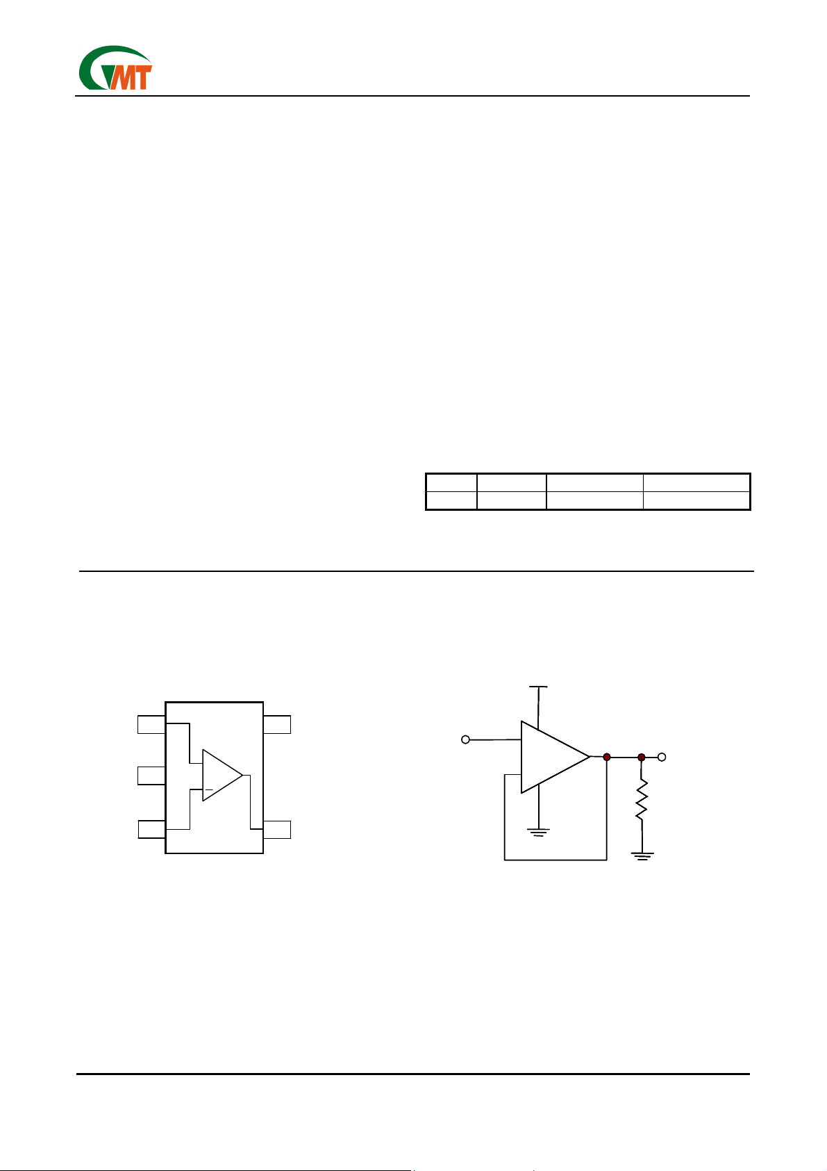
Pin Configuration Typical Application Circuit
VDD
VDD
G1214
G1214
5
IN+
IN+
V
V
SS
SS
IN-
IN-
1
1
2
2
3
3
+
+
SOT23-5
SOT23-5
V
V
DD
DD
5
5
IN
IN
OUT
OUT
4
4
1
1
3
3
5
+
+
+
+
G121
G1214
G121
G1214
-
-
2
2
4
4
RL
RL
2K
2K
OUT
OUT
Ver: 1.1
Jul 26, 2002
1
TEL: 886-3-5788833
http://www.gmt.com.tw
Page 2
Global Mixed-mode Technology Inc.
G1214
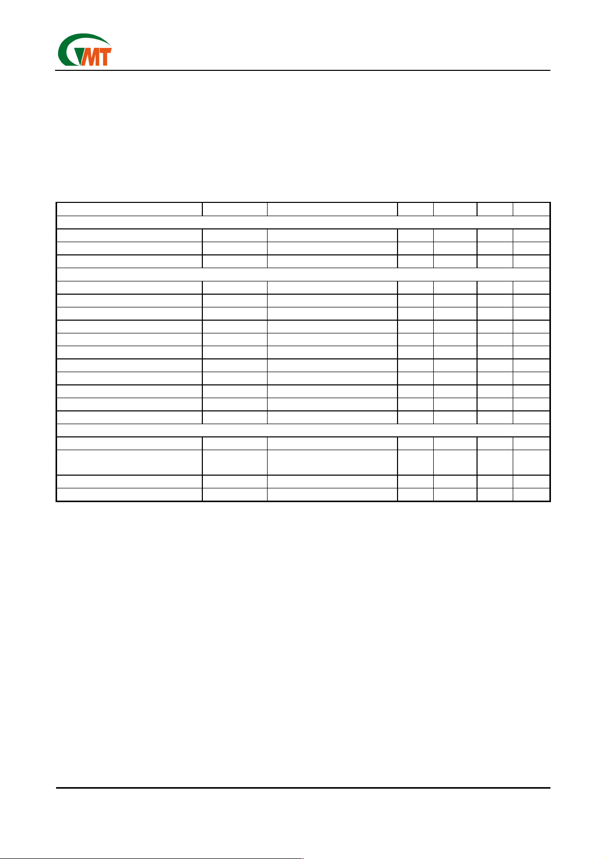
Absolute Maximum Ratings
Supply Voltage (VDD to VSS)…………………………6.5V
All Other Pins…………………(Vss-0.3V) to (V
Continuous Power Dissipation (T
=25°C)
A
+0.3V)
DD
SOT23-5…………………………………………..520mW
…………………………………………….240°C/Watt
θ
JA
Junction Temperature…………………….……….150°C
Operating Temperature Range……………..0C to 85°C
Storage Temperature Range…………..-65°C to 160°C
Lead Temperature (soldering, 10sec)…..……… 300°C
Electrical Characteristics
V
= 5V; VSS = 0V; T
DD
= 25°C; CL=10pF, RL=1k
amb
to VDD/2; unless otherwise specified.
ΩΩΩΩ
PARAMETER SYMBOL CONDITIONS MIN. TYP. MAX. UNIT
Supplies
Supply Voltage Range VDD Note1 3 5.5 V
Supply Current IDD No load - 0.5 0.7 mA
Total Power Dissipation P
DC Characteristics
Input Offset Voltage V
Common Mode Voltage VCM Inferred from CMRR test 0 - 5 V
Input Bias Current
Input Bias Current Offset
Input Resistance
Open Loop Gain
Maximum Output Current IO V
Output Voltage Swing High VOH RL = 2kΩ 4.96 4.99 V
Output Voltage Swing Low VOL RL = 2kΩ 0.012 0.04 V
Power Supply Rejection Ratio PSRR
Common-Mode Rejection Ratio CMRR
AC Characteristics
Gain-Bandwidth Product GBWP Open-loop; No Load - 6.5 - MHz
Slew-Rate SR
Phase Margin PM - 60 - deg
Maximum Output Current with THD IO THD<0.1%, RL = 16Ω 100 mA
Note1:
Guaranteed by the Power-Supply Rejection Ratio (PSRR) test
No load - 0.25 0.35 mW
tot
±5 ±15 mV
I (OS)
IB ±1.5 5 nA
IOS ±1.5 5 nA
RIN 1000 - MΩ
AV 85 95 - dB
= ±VIN x 90% 55 ±66 - mA
OUT
3V≦V
V
SS
Measured from 10% to 90% of
4V
P-P
5.5V
≦
DD
V
V
≦
DD
≦
CM
step, RL =1kΩ, CL=10pF
50 70 - dB
50 65 - dB
6.5 V/µs
Ver: 1.1
Jul 26, 2002
2
TEL: 886-3-5788833
http://www.gmt.com.tw
Page 3
Global Mixed-mode Technology Inc.
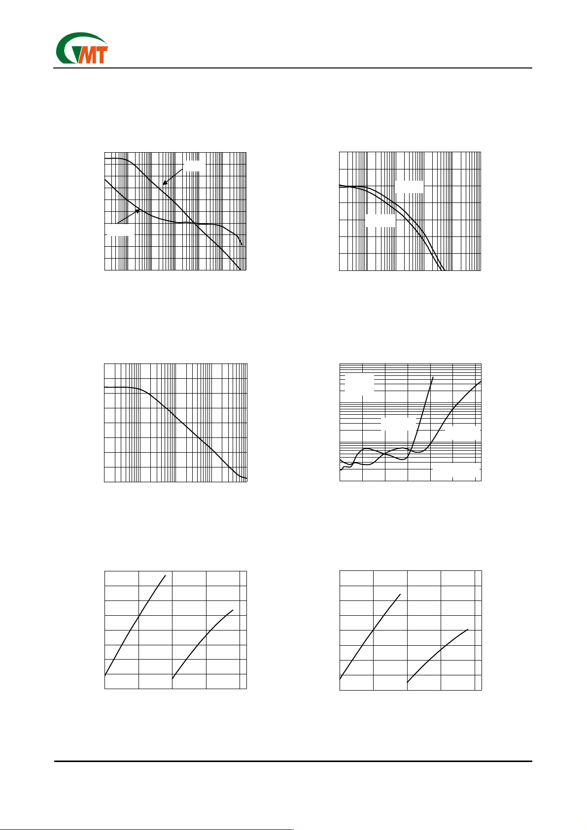
Typical Performance Characteristics
V
= 5V; VSS = 0V; T
DD
= 25°C; CL=10pF, RL=1k
amb
ΩΩΩΩ
to VDD/2; unless otherwise specified.
G1214
Open Loop Gain & Phase Margin
vs. Frequency
100
90
80
70
60
50
40
Gain(dB)
Phase
30
20
10
0
1.E-02 1.E-01 1.E+00 1.E+01 1.E+02 1.E+03 1.E+04
Frequency - kHz
Gain
CMRR vs. Frequency
80
60
225
180
135
90
Phase Margin( °)
45
0
PSRR vs. Frequency
80
PSRR-
60
PSRR (dB)
40
20
1.E-01 1.E+00 1.E+01 1.E+02 1.E+03 1.E+04
PSRR+
Frequency - kHz
Total Harmonic Distortion Plus
Noise vs.Output Power
10
f=1kHz
Av=1
1
40
CMRR (dB)
20
0
1 10 100 1000 10000
Frequency - kHz
Sinking Current vs. Vo - (VSS)
160
140
120
VDD=+5V
100
80
60
40
Sinking Current (mA)
20
0
0.1 0.6 1.1 1.6 2.1
V
DD
Vo - (VSS)
=+3V
RL=33
Ω
THD+N(%)
0.1
0.01
5 25456585105125
Output Power (mW)
RL=15
p=(Vrms)2/R
Sourcing Current vs. (VDD) - Vo
160
140
120
100
V
=+5V
DD
80
=+3V
V
60
40
Sourcing Current(mA)
20
0
0.1 0.6 1.1 1.6 2.1
DD
(VDD) - Vo
Ω
Ver: 1.1
Jul 26, 2002
3
TEL: 886-3-5788833
http://www.gmt.com.tw
Page 4
Global Mixed-mode Technology Inc.
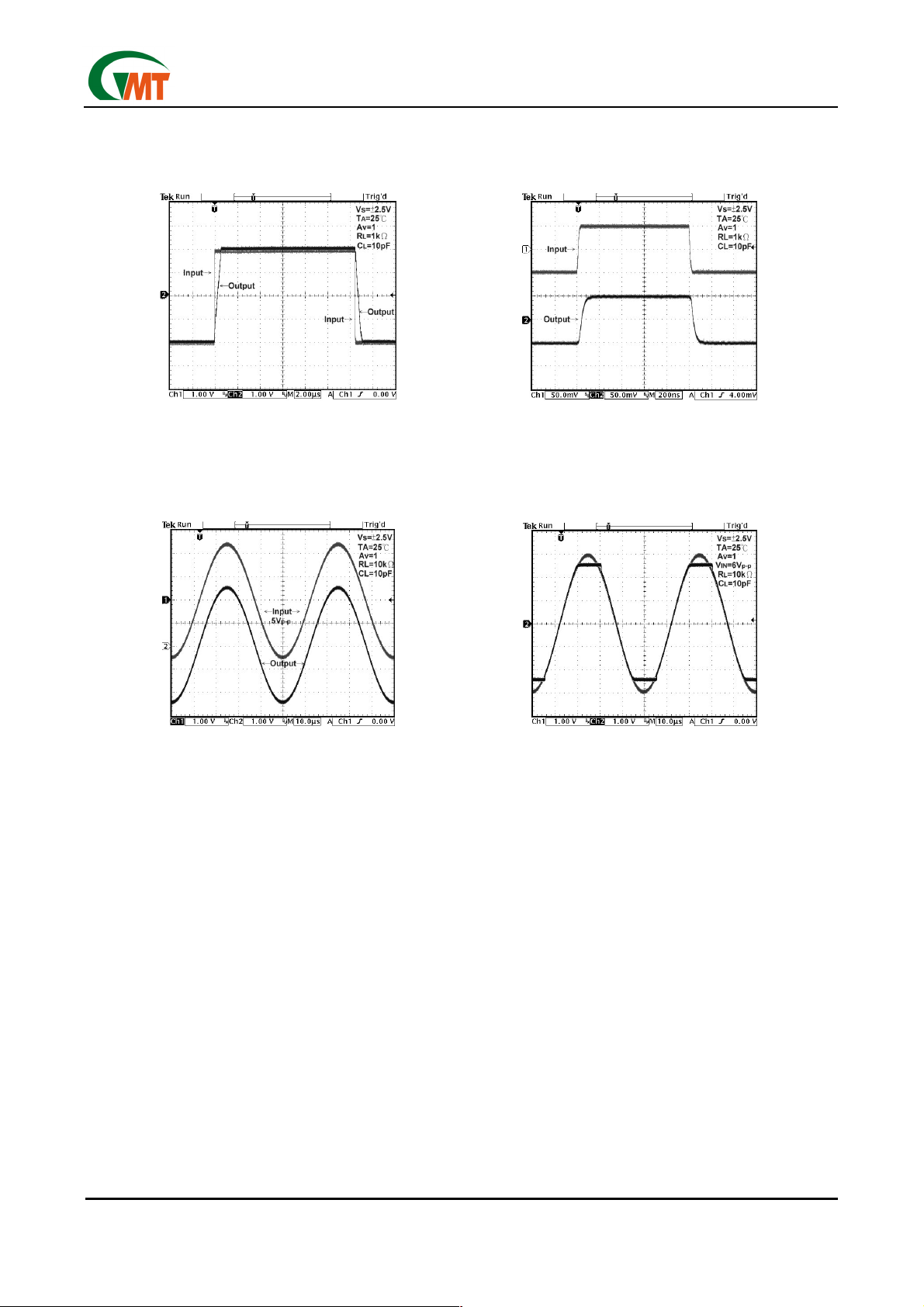
Typical Performance Characteristics
Large Signal Transient Response Small Signal Transient Response
(Continued)
G1214
Operation with Rail-to-Rail Input and Output
Operation with Beyond-the Rail Input
Ver: 1.1
Jul 26, 2002
4
TEL: 886-3-5788833
http://www.gmt.com.tw
Page 5
Global Mixed-mode Technology Inc.
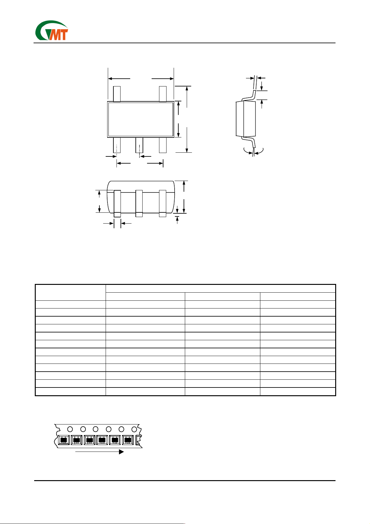
Package Information
G1214
D
H
E
e1
e
A
A2
b
A1
Note:
1. Package body sizes exclude mold flash protrusions or gate burrs
2. Tolerance ±0.1000 mm (4mil) unless otherwise specified
3. Coplanarity: 0.1000mm
4.
Dimension L is measured in gage plane
SYMBOL
A 1.00 1.10 1.30
A1 0.00 ----- 0.10
A2 0.70 0.80 0.90
b 0.35 0.40 0.50
C 0.10 0.15 0.25
D 2.70 2.90 3.10
E 1.40 1.60 1.80
e ----- 1.90(TYP) -----
e1 ----- 0.95 -----
H 2.60 2.80 3.00
L 0.37 ------ -----
1
θ
Taping Specification
(Unit: mm)
DIMENSIONS IN MILLIMETERS
MIN NOM MAX
1º 5º 9º
C
L
1
θ
Feed Direction
Feed Direction
SOT 23-5 Package Orientation
SOT 23-5 Package Orientation
GMT Inc. d oes not assume any responsibility for use of any circuitry described, no circuit patent licenses are implied and GMT Inc. reserves the right at any time without notice to change said circuitry and specifications.
Ver: 1.1
Jul 26, 2002
5
TEL: 886-3-5788833
http://www.gmt.com.tw
 Loading...