

8 x Digital Sensor Interface
Features
● Input protection against 2000 V burst/500 V surge
pulse according to IEC 801 4/5
● Input characteristic according to IEC 65 A, type 2
(24 V DC)
● Digital filter
● Serial in/out for easy cascading
● Low power dissipation
● SMD package
Type Ordering Code Package
P-DSO-24-1
FZE 1658G
FZE 1658G Q67000-A8361 P-DSO-24-1
The FZE 1658G is an integrated interface for digital sensors - i.e. proximity switches - in
industrial automation equipment. The IC has eight integrated highly protected and
failsafe inputs with status LED and a serial synchronous output for direct MC-interfacing.
Semiconductor Group 1 01.97
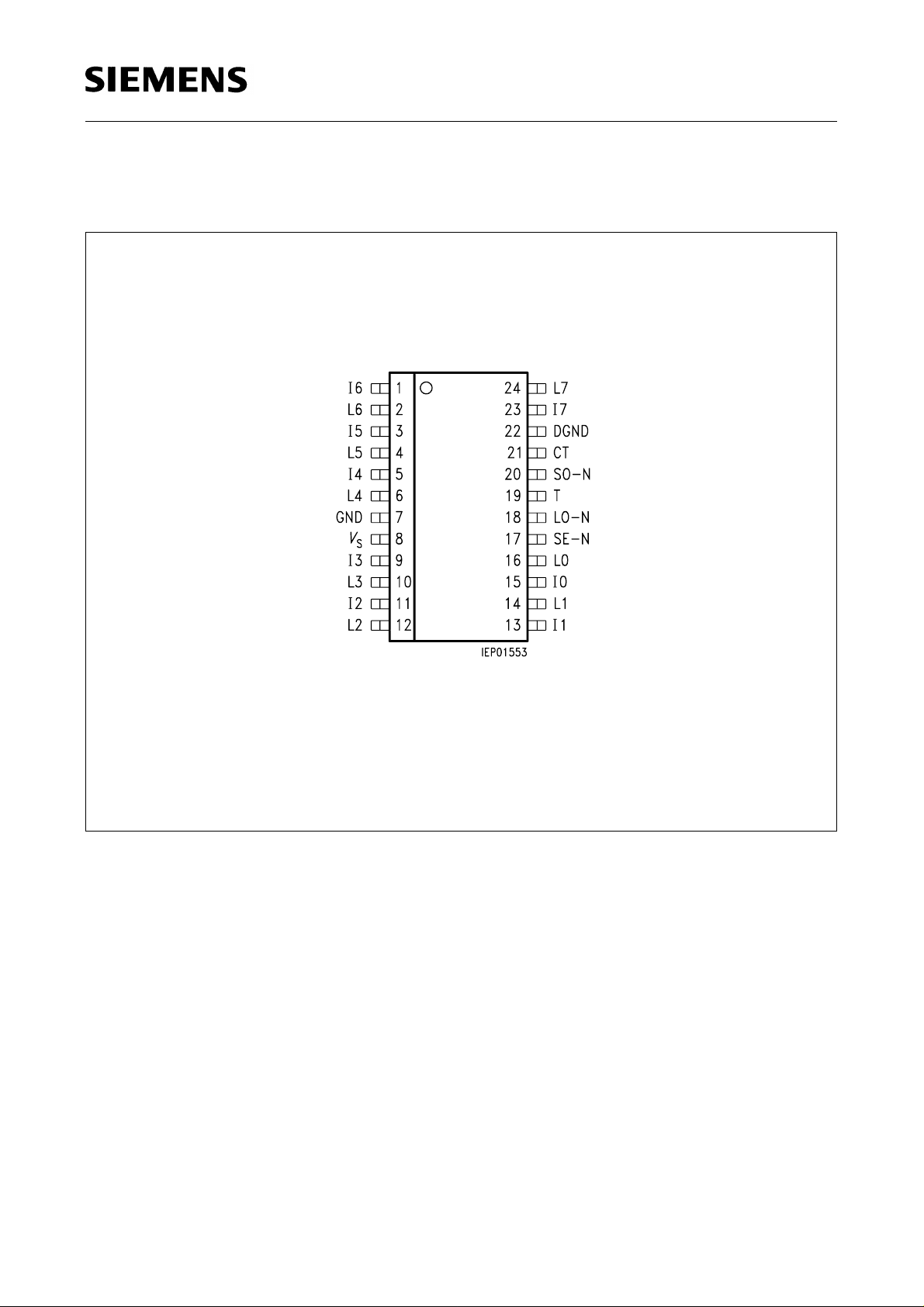
Pin Configuration
(top view)
FZE 1658G
Semiconductor Group 2
Pin Definitions and Functions
Pin Symbol Function
FZE 1658G
15, 13, 11, 9,
5, 3, 1, 23
16, 14, 12,
10, 6, 4, 2, 24
I0 - I7 Inputs for 24-V signals, in conjunction with
R
and R
V
EXT
current sink characteristic.
L0 - L7 Outputs for the status LEDs; LED lights when H-signal is
present at input.
21 CT Pin for connecting the frequency-determining capacitor for
the filter clock; also reset input if CT is connected to DGND
7 GND Ground for all 24-V signals, substrate.
22 DGND Ground for all 5-V signals, no internal connection to GND.
Any interruption of GND or DGND with the supply voltage
present may result in destruction of the device.
8
V
S
Supply voltage; undervoltage activates internal reset.
20 SO-N Serial output, open drain.
17 SE-N Extention input for serial cascading with pull-up current
source.
.
18 LO-N Latch input, edge H-L results in transfer of data from the
digital filters to the output register.
19
T
Clock for serial output, positive edge triggered.
Semiconductor Group 3
FZE 1658G
Functional Description and Application
The Integrated circuit FZE 1658G is used to detect the signal states of eight independent
input lines according to IEC 65A Type 2 (e.g. two-wire proximity switches) with a
common ground (GND). For operation in accordance with IEC 65A, it is necessary for
the device to be wired with resistors rated
tolerance and 200 ppm TK. The input device has the following characteristics:
– Minimization of power dissipation due to constant current characteristic
– Inputs protected against reverse polarity and transient overvoltages
– Status LED output for each input
– Digital averaging of the input signals to suppress interference pulses
– Serial output of the detected signals (cascadable)
Maximum voltage ratings at inputs D0 ... D7 within test circuit 2.
Voltage Range Notes
R
= 820 Ω and R
V
= 4.4 kΩ with ± 2%
EXT
DC voltage – 3 V … + 32 V
–32V … +32V
Overvoltage 500 ms – 3 V … + 35 V
–35V … +35V
Overvoltage 1.3 ms
to VDE 0160
Surge pulse 50 µs
to IEC 801-5,
Z
= 2 Ω
i
Burst pulse 50 ns
to IEC 801-4,
1)
Non-destructive in temperature range 15 °C ≤ TA≤ 35 °C.
2)
In temperature range 15 °C ≤ TA≤ 35 °C:
Data retained if the supply voltage remains within the operating range; without supply voltage
non-destructive.
Z
= 50 Ω
i
– 3 V … + 55 V
± 55
± 0.5 kV
± 2kV
full function
non-destructive, no latch-up
full function
non-destructive, no latch-up
full function
non-destructive, no latch-up
1)
2)
The rated voltage may be applied to all inputs simultaneously.
The values given in the table may be regarded as guaranteed, but are only checked as
part of a qualification (no 100 % series testing).
Within the application circuit given the same voltage ratings as above apply for the
supply line.
Semiconductor Group 4

FZE 1658G
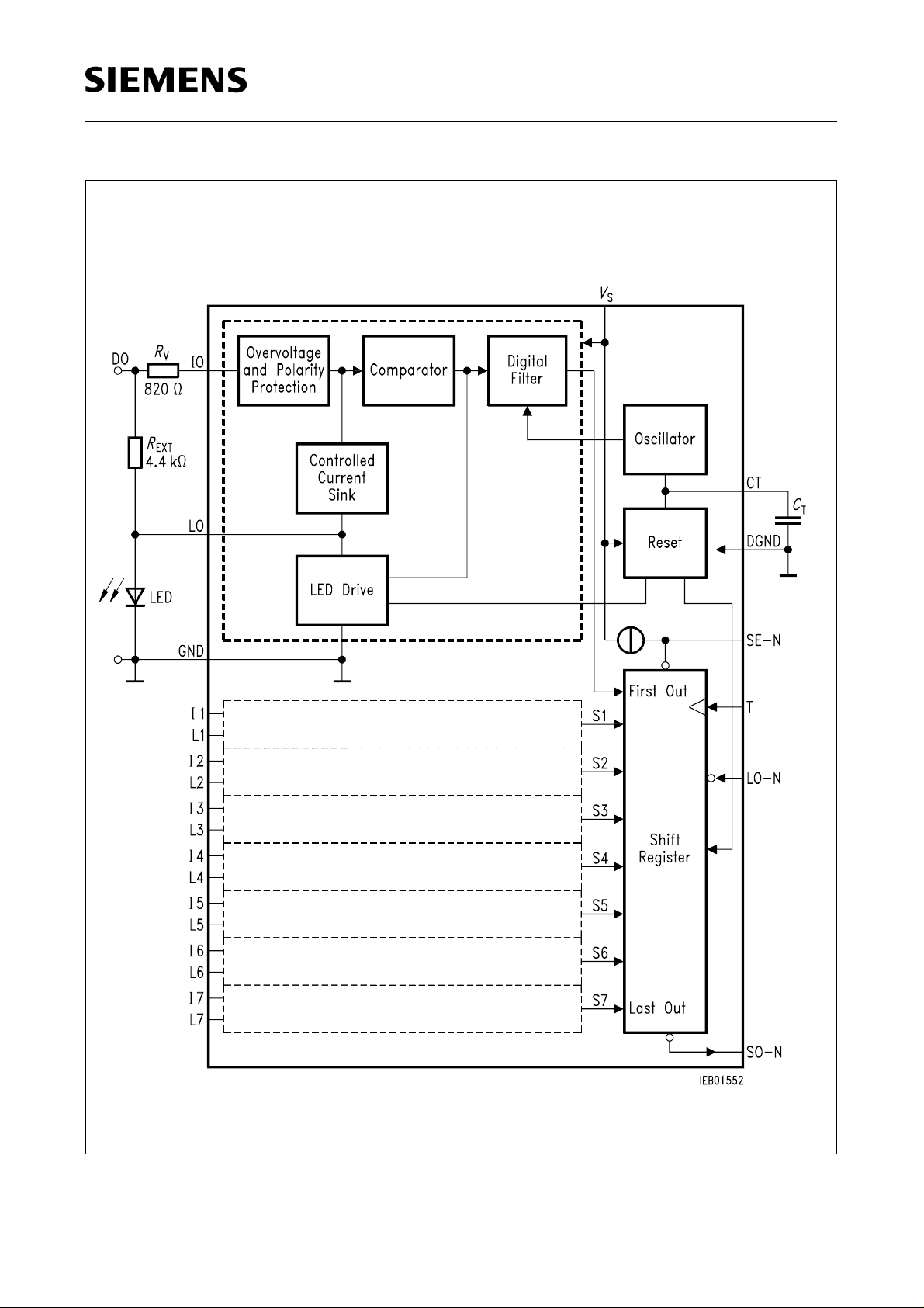
Circuit Description
In IEC 65A, the following values are specified for 24-VDC input stages of type 2:
Level Input Voltage Input Current
1
0
min. 11 V
max. 11 V
min. 6 mA
max. 2 mA
or max. 5 V
The current in the input circuit is determined by the switching element in state “0” and by
characteristics of the input stage in state “1”.
The octal input device FZE 1658G is intended for a configuration comprising two
specified external resistors per channel, as shown in the block diagram. As a result the
power dissipation within the P-DSO-24-1 package is at a minimum.
R
The voltage dependent current through the external resistor
is compensated by a
EXT
negative differential resistance of the current sink across pins E and L, therefore input D
behaves like a constant current sink.
The comparator assigns level 1 or 0 to the voltage present at input E. To improve
interference protection, the comparator is provided with hysteresis and a delay element.
A status LED is connected in series with the input circuit (R
and current sink). The
EXT
LED drive short-circuits the status LED if the comparator detects “0”. A constant current
sink in parallel with the LED reduces the operating current of the LED, and a voltage
limiter ensures that the input circuit remains operational if the LED is interrupted. The
specified switching thresholds may change if the LED is interrupted.
For each channel a digital filter is provided which samples the comparator signal at a rate
provided by the clock oscillator. The digital filter is designed as a 5-section shift register.
If any four out of 5 sampling values are identical, the output S changes to the
corresponding state.
On a falling edge at input LO-N, the parallel data S0 - S7 are clocked into the output shift
register. The data can be shifted out serially to the output SO-N by the clock signal T,
with a “1” at the input being represented by a L-signal at the output SO-N. The serial
interface of the shift register fits the synchronous interface of the 8051 microcontroller
(see diagram Serial Data Output Function). By connecting output SO-N to input SE-
N of the next device, several FZE 1658G can be cascaded (see Application Circuit).
SO-N is designed as an open-drain output. SE-N has an internal pull-up current source.
Inputs SE-N, T and SO-N have Schmitt trigger characteristics. The device has separate
ground pins for the input circuitry (GND) and for the logic (DGND). If the supply voltage
falls below
V
or CT is connected to DGND, the output shift register will be cleared and
USR
the output SO-N disabled. If the supply voltage is too low, the LED drives will also be
disabled, i.e. the LED lights as soon as current flows in the input circuit.
Semiconductor Group 5
FZE 1658G
Block Diagram
Semiconductor Group 6

FZE 1658G
Absolute Maximum Ratings
T
= – 40 to 150 °C
j
Parameter Symbol Limit Values Unit Notes
min. max.
Transient input current
inputs I0 - I7
Ground current
Junction temperature
Storage temperature
Thermal resistance
System/air
Transient thermal resistance;
Same current through all
inputs I0 - I7
Supply voltage
Ground offset DGND to GND
I
I
I
GND
T
T
R
Z
Z
V
V
j
S
thja
th
th
S
DGND
– 0.6
– 1.2
– 2.5
–5
–10
0.6
1.2
2.5
5
10
A
A
A
A
A
t
50 %
t
50 %
t
50 %
t
50 %
t
50 %
– 40 150 °C
– 50 125 °C
95 K/W soldered-in
0.15
0.4
K/W
K/W
50 µs pulse
120 µs pulse
– 0.3 65 V
–4 4 V V
≤ 50 µs
≤ 1.2 µs
≤ 50 ns
≤ 50 µs
≤ 50 ns
DGND
< V
S
Current at the LED outputs I
Voltage at
V
T, LO-N, SO-N, SE-N
Capacitance at CT
C
ESD voltage 100 pF / 1.5 kΩ V
L
LOG
CT
ESD
–15
– 500
– 250
– 125
–4
– 0.3
15
500
250
125
9
9
2 µF when VS falls
1000 1000 V MIL Std. 883
mA
mA
mA
mA
t
50 %
t
50 %
t
50 %
≤ 50 µs
≤ 1.2 µs
≤ 50 µs
V
V referred to DGND
below
V
CT
Meth. 3015
All voltages are, unless otherwise specified, referred to GND. This also applies to the
operating range and the characteristics.
Semiconductor Group 7

FZE 1658G
Operating Range
Parameter Symbol Limit Values Unit Notes
min. max.
Supply voltage
V
Supply voltage rise SR
Supply voltage
V
GND potential difference V
Input terminal current
Input voltage SE-N, T, LO-N
I
V
IT
V
Input current SE-N, T, LO-N
Junction temperature
Ambient temperature
Clock frequency f
I
I
T
T
T
S
VS
S-VDGND
DGND
IH
IL
j
A
10 48 V Note power
dissipation
1)
– 0.1 1 V/µs
9V
2)
– 1.5 1.5 V
–10 10 mA
2.8
– 0.5
6
1.7
V
V
– 1 1 mA Clamp current
– 25 150 °C
– 25 105 °C Dependent on R
1 MHz
th
Clock pulse width H or L
SE-N set up time to T ↑
LO-N set up time to T ↑
SE-N, LO-N, T rise and fall time
t
t
t
t
TH
VSE
VLO
, t
r
, t
TL
300 ns
300 ns
1.2 µs
f
3 µs
3)
within thresholds
1)
Input voltages may rise before the supply voltage.
Full function at VS> V
2)
Limits GND potential difference at minimum supply voltage.
3)
Also applies to several cascaded FZE 1658G (note dependence with clock frequency).
For definition of timing items, see timing diagram.
(see Characteristics).
VSRO
Semiconductor Group 8

FZE 1658G
Characteristics
V
= 15 Vto 30 V; V
S
Parameter Symbol Limit Values Unit Test Condition Test
Inputs I0 - I7 or D0 - D7 Respectively
= 0, Tj = – 25 °C<Tj< 125 °C
DGND
min. typ. max.
Circuit
Switching
threshold H
Switching
threshold L
Hysteresis
Switching
threshold L
Input current
Input current
Input current
Input clamp voltage
V
V
V
I
I
I
I
V
DH
DL
DHY
DLL
DH
DL
IC +
IT +
10.851)V2
8VV
1VV
2.5 mA I
1)
6.2
8mAV
57mAV
1mAV
35 75 V II = 10 mA,
≤2.2 V 2
L
≤2.2 V 2
L
= 0 2
LED
≤3.5 V,
L
V
= 11 … 30 V
D
=V
LL
= 5 V
,
2)
2)
L
V
D
= 30 V
I
T
= 25 °C
j
2
2
1
1
Input current
Input clamp voltage
1)
Headroom to IEC 65 A for tolerance of ext. resistor.
2)
Also valid at VS = 0.
I
V
IC –
IT –
–1 mA VI = – 30 V
– 75 – 35 V II = – 10 mA,
Semiconductor Group 9
T
= 25 °C
j
2)
2)
1
1

FZE 1658G
Characteristics (cont’d)
V
= 15 Vto 30 V; V
S
Parameter Symbol Limit Values Unit Test Condition Test
LED Drive L0 - L7
= 0, Tj = – 25 °C<Tj< 125 °C
DGND
min. typ. max.
Circuit
Open-load voltage
“Low”- voltage
Output current
Output current
Power down
output current
Propagation delay
rising and falling
edge
Oscillator
V
V
I
I
I
t
LO
LL
LED
LED
L
DL
3.5 5 V VD = 24 V,
I
= 0
LED
0 0.75 V VD = 5 V,
I
= 0
LED
35mAV
= 11 … 30 V,
D
V
= 1.5 … 3 V
L
1.5 6 mA VD = 11 … 30 V,
V
= 1.2 … 3.5 V
L
– 0.12 mA VS < V
7.5 75 µs VD = 12V
VSRU
←
→
7V
2
2
2
2
1
2
CT source/sink
I
CT
150 250 µA1
current
Frequency
Upper switching
f
V
CT
CTP
1 1.5 kHz CT = 39 nF 2
3.3 4.3 V 2
threshold
Lower switching
V
CTN
1.4 2.2 V 2
threshold
Reset threshold
Reset input current
Signal delay
V
I
t
CTR
CTR
DFI
0.8 1.4 V 1
– 300 – 150 µA VCT = 0.8 V 1
24msC
Semiconductor Group 10
= 39 nF 2
T

FZE 1658G
Characteristics (cont’d)
V
= 15 Vto 30 V; V
S
Parameter Symbol Limit Values Unit Test Condition Test
5-V Logic
= 0, Tj = – 25 °C<Tj< 125 °C
DGND
min. typ. max.
Circuit
Input current
T, LO-N
Input current SE-N
Input current
T, LO-N, SE-N
Input capacitance
L-output current
SO-N
L-output level SO-N
H-leakage current
SO-N
Output
capacitance SO-N
Rise/fall time of
output current
SO-N
I
I
I
C
I
V
I
C
t
rSO
I
ISE
I0
I
SOL
SOL
SOH
SOH
, t
–10 10 µA Vi = 0 … 5 V 1
– 600 – 400 µA Vi = 0 … 3 V 1
020µAV
= 0 … 5 V
i
V
= 0 V
S
10 pF 1
5.5 8 mA VQ = 3 … 5 V 1
0 0.5 V ISO = 2 mA 1
050µAV
= 5 V 1
SO
20 pF VSO = 1.5 V 1
fSO
50 ns VSO = 2.5 V 1
1
Delay time
t
SOT
T to SO-N
(see timing
diagram)
Delay time
t
SOLO
LO-N to SO-N
(see timing
diagram)
Hysteresis SE-N,
60 mV no 100% testing
LO-N
Semiconductor Group 11
150 ns VSO = 2.5 V 1
300 ns VSO = 2.5 V 1

FZE 1658G
Characteristics (cont’d)
V
= 15 Vto 30 V; V
S
Parameter Symbol Limit Values Unit Test Condition Test
= 0, Tj = – 25 °C<Tj< 125 °C
DGND
min. typ. max.
Circuit
Hysteresis
Clock input
Voltage Supply
Current drain static
Current drain
during serial
readout
Current drain
during high supply
voltage
Logic ground
current
I
S
I
S
I
SMAX
I
DGND
200 mV no 100% testing
25mAV
26mAV
7mAV
– 2.5 0 mA V
= 10 … 30 V
S
V
= 5 V
LO-N
V
= 5 V
T
I
= 0
SE-N
= 10 … 40 V
S
V
= 0 V
LO-N
f
= 1 MHz
T
< 45 V 2
S
=
DGND
– 1.5 … 1.5 V,
LO-N = H
2
2
1
Under voltage
V
VSRO
lockout
V
V
VSRU
VSRH
8
0.2
Semiconductor Group 12
10 V
V
V
upper switching
treshold
lower switching
threshold
hysteresis
2
2
2

FZE 1658G
Test Circuit 1
Test Circuit 2
Semiconductor Group 13

Application Circuit
FZE 1658G
Supply Voltage Decoupling Circuit
Cascading Multiple FZE 1658G
Semiconductor Group 14

FZE 1658G
Serial Data Output Function
Semiconductor Group 15

FZE 1658G
Timing Diagram
Semiconductor Group 16

Input Characteristic with Worst-Case
Values per IEC 65A Input D Rest Circuit D
FZE 1658G
Semiconductor Group 17

Package Outlines
Plastic-Package, P-DSO-24-1 (SMD)
(Plastic Dual Small Outline Package)
FZE 1658G
Sorts of Packing
Package outlines for tubes, trays etc. are contained in our
Data Book “Package Information”.
SMD = Surface Mounted Device
Semiconductor Group 18
GPS05144
Dimensions in mm
 Loading...