

Page 1
查询FX614供应商
CML Semiconductor Products
Bell 202 Compatible Modem FX614
1.0 Features
•• 1200bits/sec 1/2 Duplex Bell 202 compatible Modem with:
D/614/4 October 1997
Advance Information
•• Optional 5bits/sec and
150bits/sec Back Channel
•• Optional 1200bits/sec Data
Retiming Facility
•• 3.0 to 5.5V Supply; 1.0mA at 3V
'Zero-Power' Mode; 1
µµA
1.1 Brief Description
•• Optional Line Equalisation
•• -40°C to +85°C Operating
Temperature
•• 16-pin SOIC and DIL Packages
•• 3.58MHz Xtal/Clock Rate
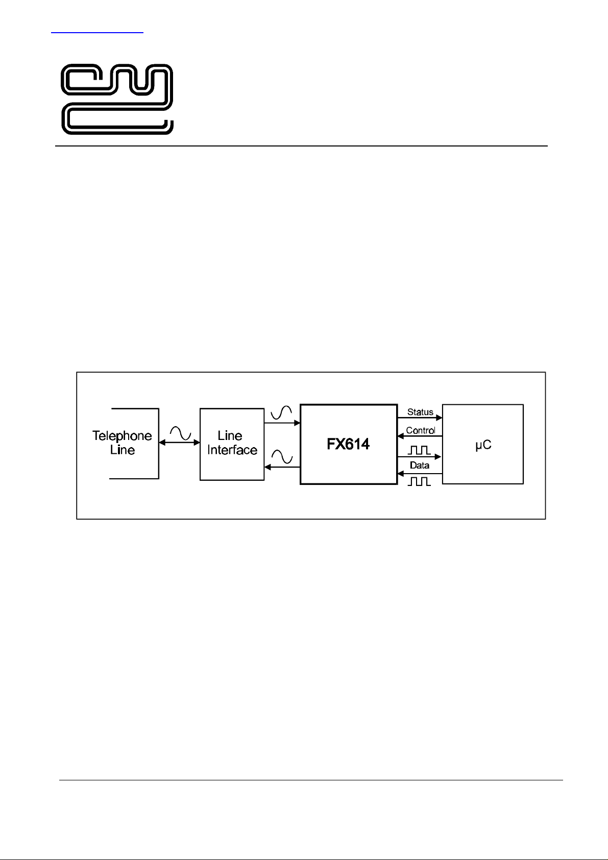
The FX614 is a low power CMOS integrated circuit for the reception or transmission of asynchronous
1200bits/sec data and is suitable for use in Bell 202 type systems. It is also capable of generating the
5bits/sec or 150bits/sec 'back channel'.
The device incorporates an optional Tx and Rx data retiming function that removes the need for a UART in the
associated
this is controlled by an external logic level.
The FX614 may be used in a wide range of telephone telemetry systems. With a low operating voltage of
3.0V, a very low current 'sleep' mode (1
terminal and line powered applications. A 3.58MHz standard Xtal/Clock rate is required and the device
operates from a 3.0V to 5.5V supply. Both SOIC (D4) and Plastic DIL (P3) 16-pin package types are available.
1997 Consumer Microcircuits Limited
µC when operating at 1200bits/sec. An optional line equaliser is incorporated into the receive path,
µA) and an operating current of 1mA the device is ideal for portable,
Page 2

Bell 202 Compatible Modem FX614
CONTENTS
Section Page
1.0 Features ......................................................................................................1
1.1 Brief Description.........................................................................................1
1.2 Block Diagram ............................................................................................3
1.3 Signal List...................................................................................................3
1.4 External Components.................................................................................5
1.5 General Description....................................................................................5
1.5.1 Xtal Osc and Clock Dividers.......................................................5
1.5.2 Mode Control Logic ....................................................................6
1.5.3 Rx Input Amplifier.......................................................................6
1.5.4 Receive Filter and Equaliser.......................................................6
1.5.5 Energy Detector ..........................................................................7
1.5.6 FSK Demodulator ................................................................ ........7
1.5.7 FSK Modulator and Transmit Filter ................................ ............7
1.5.8 Rx Data Retiming ........................................................................9
1.5.9 Tx Data Retiming ................................................................ .......10
1.6 Application Notes.....................................................................................12
1.6.1 Line Interface.............................................................................12
1.7 Performance Specification.......................................................................13
1.7.1 Electrical Performance..............................................................13
1.7.2 Packaging..................................................................................16
1997 Consumer Microcircuits Limited 2 D/614/4
Page 3
Bell 202 Compatible Modem FX614
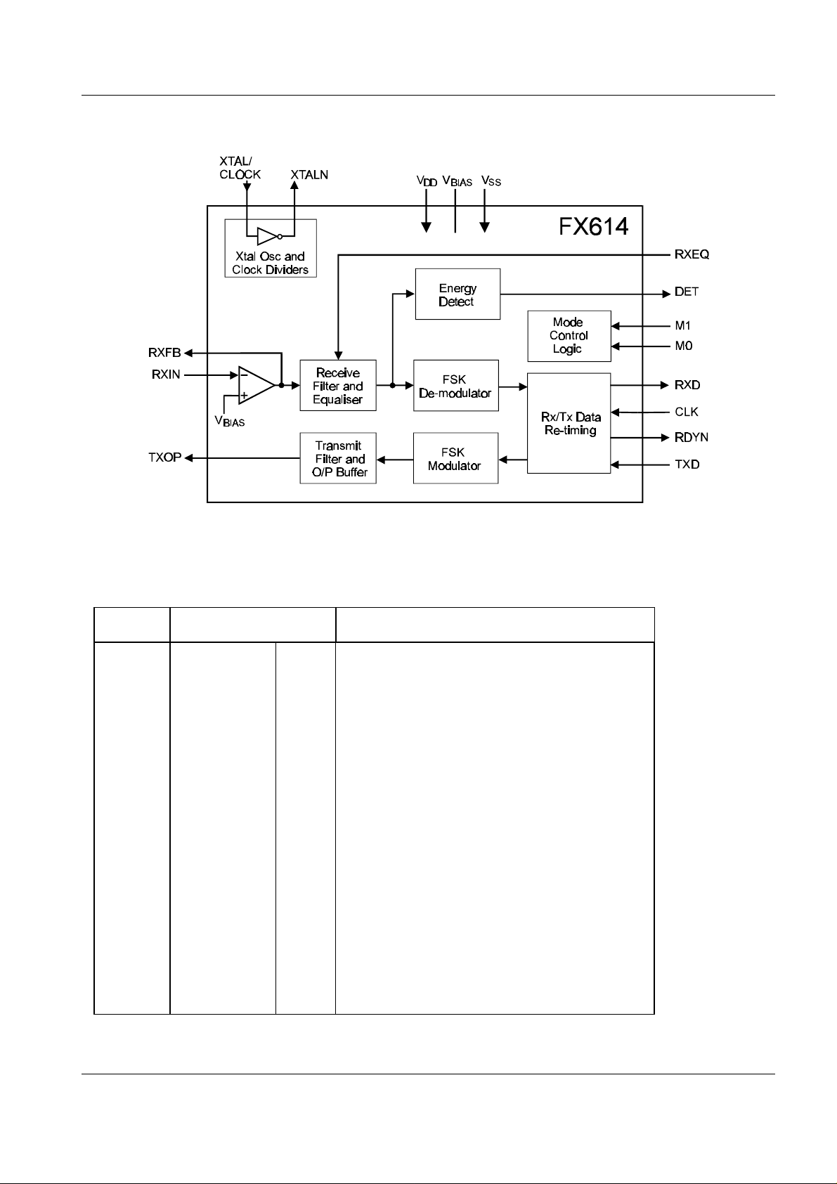
1.2 Block Diagram
1.3 Signal List
FX614
D4/P3
Pin No. Name Type
1 XTALN O/P The output of the on-chip Xtal oscillator inverter.
2 XTAL/CLOCK I/P The input to the on-chip Xtal oscillator inverter.
3 M0 I/P A logic level input for setting the mode of the
4 M1 I/P A logic level input for setting the mode of the
5 RXIN I/P Input to the Rx input amplifier.
6 RXFB O/P Output of the Rx input amplifier, and the input to
Signal Description
Figure 1 Block Diagram
device. See section 1.5.2.
device. See section 1.5.2.
the Rx filter.
7 TXOP O/P The output of the FSK generator.
8 V
1997 Consumer Microcircuits Limited 3 D/614/4
SS
Power The negative supply rail (ground).
Page 4
Bell 202 Compatible Modem FX614
FX614
D4/P3
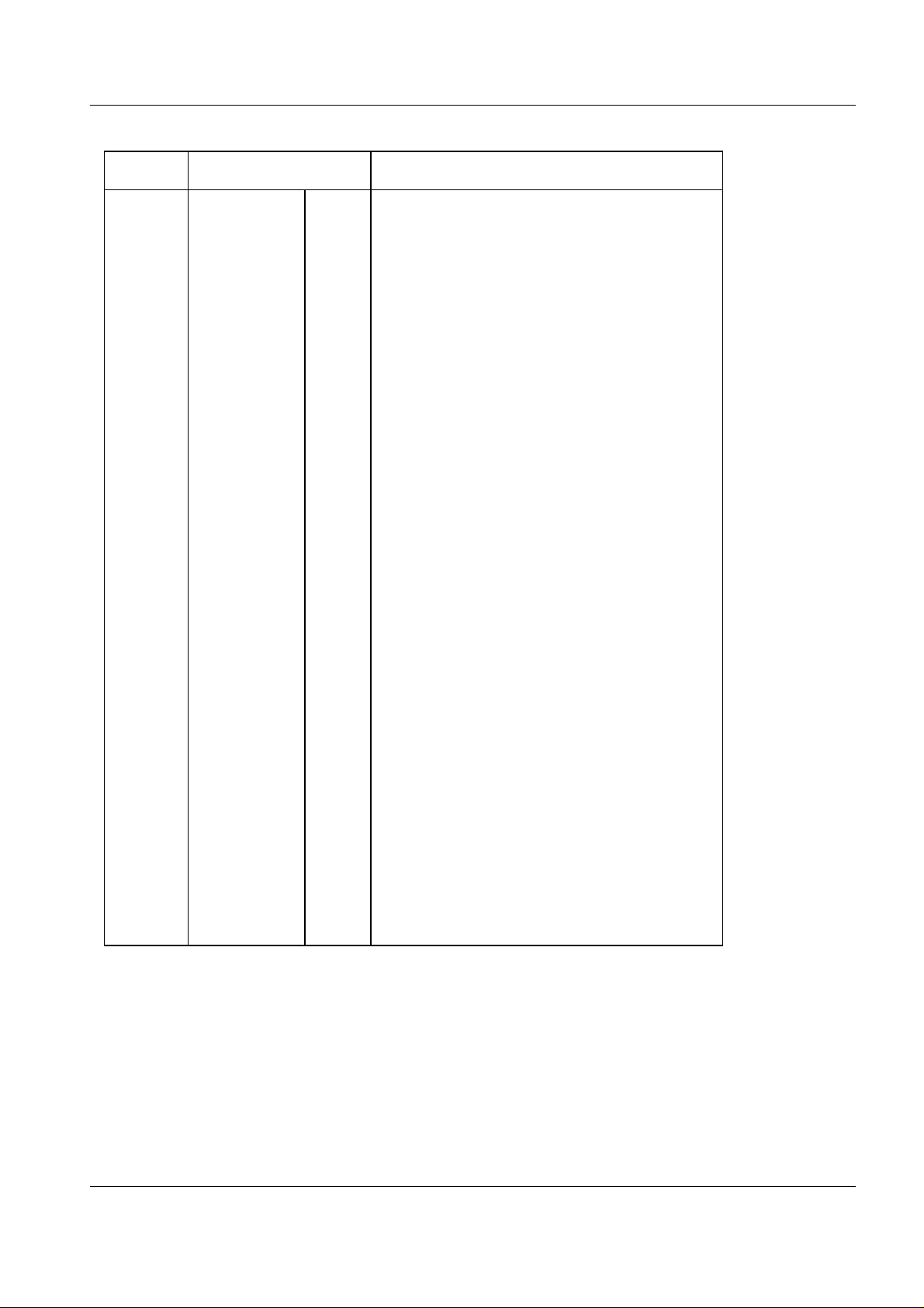
Signal Description
Pin No. Name Type
9 V
BIAS
O/P Internally generated bias voltage, held at VDD/2
when the device is not in 'Zero-Power' mode.
Should be decoupled to VSS by a capacitor
mounted close to the device pins.
10 RXEQ I/P A logic level input for enabling/disabling the
equaliser in the receive filter. See section 1.5.4.
11 TXD I/P A logic level input for either the raw input to the
FSK Modulator or data to be re-timed depending
on the state of the M0, M1 and CLK inputs. See
section 1.5.9.
12 CLK I/P A logic level input which may be used to clock
data bits in or out of the FSK Data Retiming
block.
13 RXD O/P A logic level output carrying either the raw
output of the FSK Demodulator or re-timed
characters depending on the state of the M0, M1
and CLK inputs. See section 1.5.8.
14 DET O/P A logic level output of the on-chip Energy Detect
circuit.
15 RDYN O/P "Ready for data transfer" output of the on-chip
data retiming circuit. This open-drain active low
output may be used as an Interrupt
Request/Wake-up input to the associated
µC.
An external pull-up resistor should be connected
between this output and VDD.
16 V
DD
Power The positive supply rail. Levels and thresholds
within the device are proportional to this voltage.
Should be decoupled to VSS by a capacitor
mounted close to the device pins.
Notes: I/P = Input
O/P = Output
This device is capable of detecting and decoding small amplitude signals. To achieve this V
DD
and V
BIAS
decoupling and protecting the receive path from extraneous in-band signals are very important. It is
recommended that the decoupling capacitors are placed so that connections between them and the device
pins are as short as practicable. A ground plane protecting the receive path will help attenuate interfering
signals.
1997 Consumer Microcircuits Limited 4 D/614/4
Page 5
Bell 202 Compatible Modem FX614
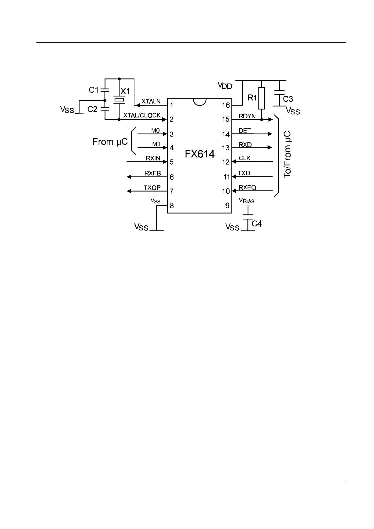
1.4 External Components
R1
100k
Ω
X1 3.579545MHz C3
Resistors
±5%, capacitors ±10% unless otherwise stated.
C1, C2 18pF
µF
0.1
C4
0.1
µF
Figure 2 Recommended External Components for Typical Application
1.5 General Description
1.5.1 Xtal Osc and Clock Dividers
Frequency and timing accuracy of the FX614 is determined by a 3.579545MHz clock present at the
XTAL/CLOCK pin. This may be generated by the on-chip oscillator inverter using the external components C1,
C2 and X1 of Figure 2, or may be supplied from an external source to the XTAL/CLOCK input. If supplied from
an external source, C1, C2 and X1 should not be fitted.
The on-chip oscillator is turned off in the 'Zero-Power' mode.
If the clock is provided by an external source which is not always running, then the 'Zero-Power' mode must be
set when the clock is not available. Failure to observe this rule may cause a significant rise in the supply
current drawn by FX614 as well as generating undefined states of the RXD, DET and RDYN outputs.
1997 Consumer Microcircuits Limited 5 D/614/4
Page 6

Bell 202 Compatible Modem FX614
1.5.2 Mode Control Logic
The FX614's operating mode is determined by the logic levels applied to the M0 and M1 input pins:
M1 M0 Rx Mode Tx Mode
Data Retime
[1]
0 0 1200bits/sec 150bits/sec Rx
0 1 Off 1200bits/sec Tx
1 0 1200bits/sec Off / 5bits/sec Rx
1 1 'Zero-Power' -
[1] If enabled.
In the 'Zero-Power' (ZP) mode, power is removed from all internal circuitry. When leaving the 'ZP' mode there
must be a delay of 20ms before any Tx data is passed to, or Rx data read from, the device to allow the bias
level, filters and oscillator to stabilise. On applying power to the device the mode must be set to 'ZP', i.e. M0 =
'1', M1 = '1', until V
has stabilised.
DD
1.5.3 Rx Input Amplifier
This amplifier is used to adjust the received signal to the correct amplitude for the FSK receiver and Energy
Detect circuits (see section 1.6.1).
1.5.4 Receive Filter and Equaliser
Is used to attenuate out of band noise and interfering signals, especially the locally generated transmit tones
which might otherwise reach the 1200bits/sec FSK Demodulator and Energy Detector circuits. This block also
includes a switchable equaliser section. When the RXEQ pin is low, the overall group delay of the receive filter
is flat over the 1200bits/sec frequency range. If the RXEQ pin is high the receive filter's typical overall group
delay will be as shown in Figure 3.
Figure 3 Rx Equaliser Group Delay (RXEQ = '1') wrt 1700Hz
1997 Consumer Microcircuits Limited 6 D/614/4
Page 7
Bell 202 Compatible Modem FX614
1.5.5 Energy Detector
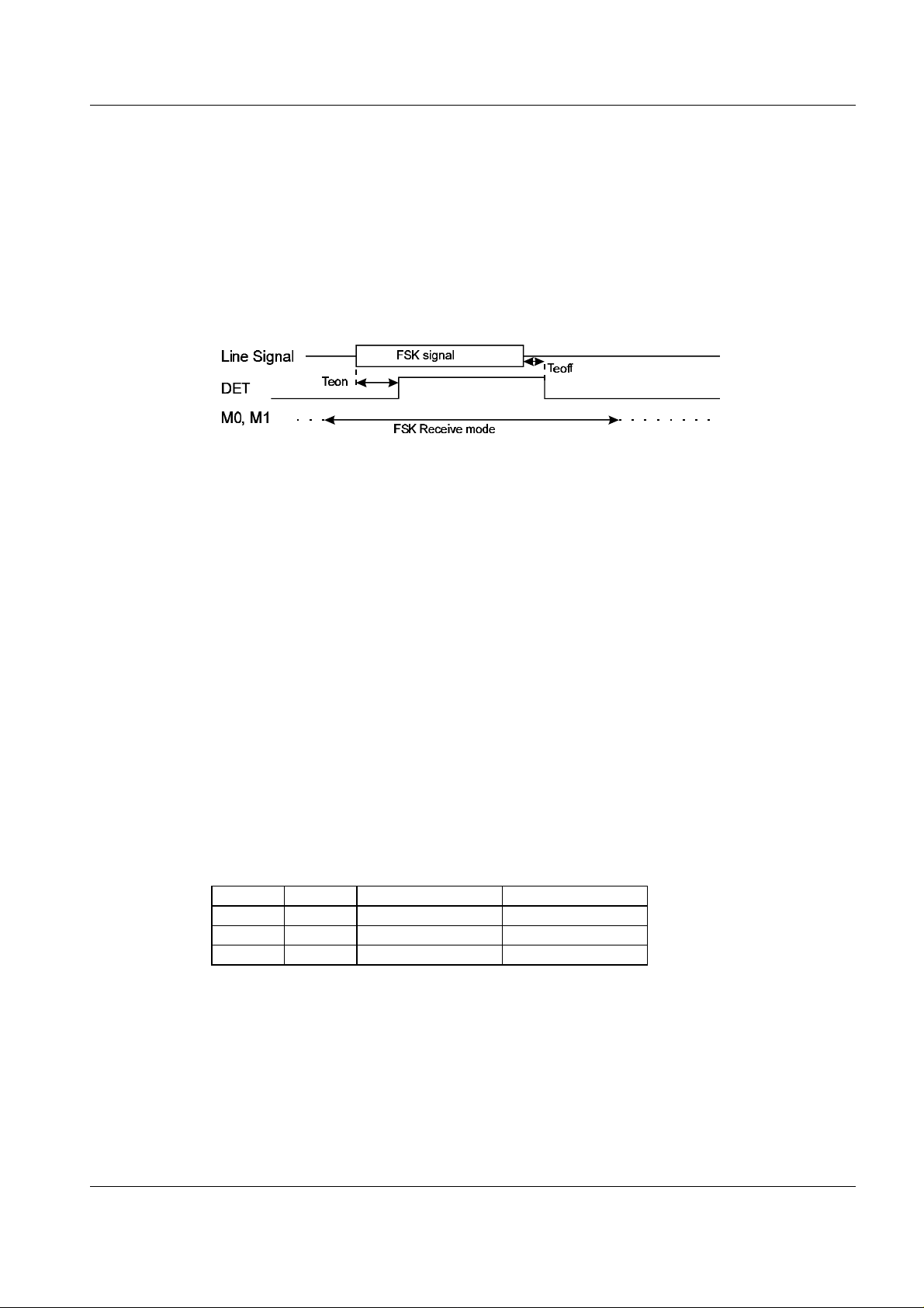
This block operates by measuring the level of the signal at the output of the Receive Filter, and comparing it
against a preset threshold.
The DET output will be set high when the level has exceeded the threshold for sufficient time. Amplitude and
time hysteresis are used to reduce chattering of the DET output in marginal conditions.
Note that this circuit may also respond to non-FSK signals such as speech.
See section 1.7.1 for definitions of Teon and Teoff
Figure 4 FSK Level Detector Operation
1.5.6 FSK Demodulator
This block converts the 1200bits/sec FSK input signal to a logic level received data signal which is output via
the RXD pin as long as the Data Retiming function is not enabled (see section 1.5.8). This output does not
depend on the state of the DET output.
When the Rx 1200bits/sec mode is 'Off' or in 'ZP' the DET and RXD pins are held low.
Note that in the absence of a valid FSK signal, the demodulator may falsely interpret speech or other
extraneous signals as data. For this reason it is advised that the RXD pin is read only when data is expected.
1.5.7 FSK Modulator and Transmit Filter
These blocks produce a tone according to the TXD, M0 and M1 inputs as shown in the table below, assuming
data retiming is not being used:
M1 M0 TXD = '0' TXD = '1'
1 1 - 1 0 0Hz
[1]
387Hz
0 0 487Hz 387Hz
0 1 2200Hz 1200Hz
Note: [1] TXOP held at approx VDD/2.
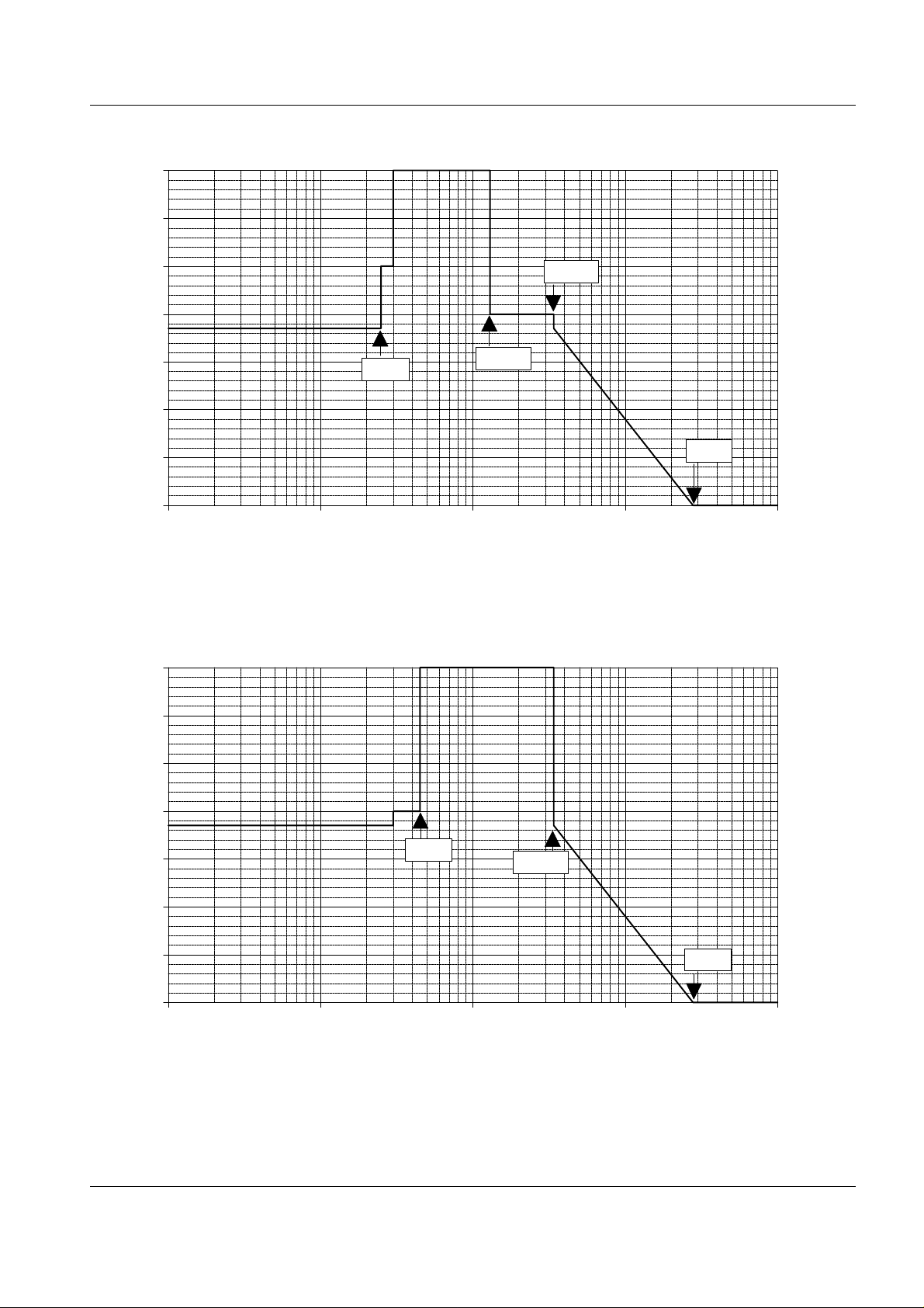
When modulated at the appropriate baud rates, the Transmit Filter and associated external components (see
section 1.6.1) limit the FSK out of band energy sent to the line in accordance with Figures 5a and 5b,
assuming that the signal on the line is at -6dBm or less.
1997 Consumer Microcircuits Limited 7 D/614/4
Page 8
Bell 202 Compatible Modem FX614
0
dBm
-10
-20
-30
-40
-50
-60
-70
10 100 1000 10000 100000
250 Hz
1300 Hz
3400 Hz
28 kHz
Frequency / Hz
Figure 5a Tx limits at 5bits/sec or 150bits/sec rate
0
dBm
-10
-20
-30
-40
-50
-60
-70
10 100 1000 10000 100000
450 Hz
3400 Hz
28 kHz
Frequency / Hz
Figure 5b Tx limits at 1200bits/sec rate
1997 Consumer Microcircuits Limited 8 D/614/4
Page 9

Bell 202 Compatible Modem FX614
1.5.8 Rx Data Retiming
This function may be used when the received data consists of 1200bits/sec asynchronous characters, each
character consisting of one start bit followed by a minimum of 9 formatted bits as shown in the table below.
Data bits Parity bits Stop bits
7 0 >=2
7 1 >=1
8 0 >=1
8 1 >=1
9 0 >=1
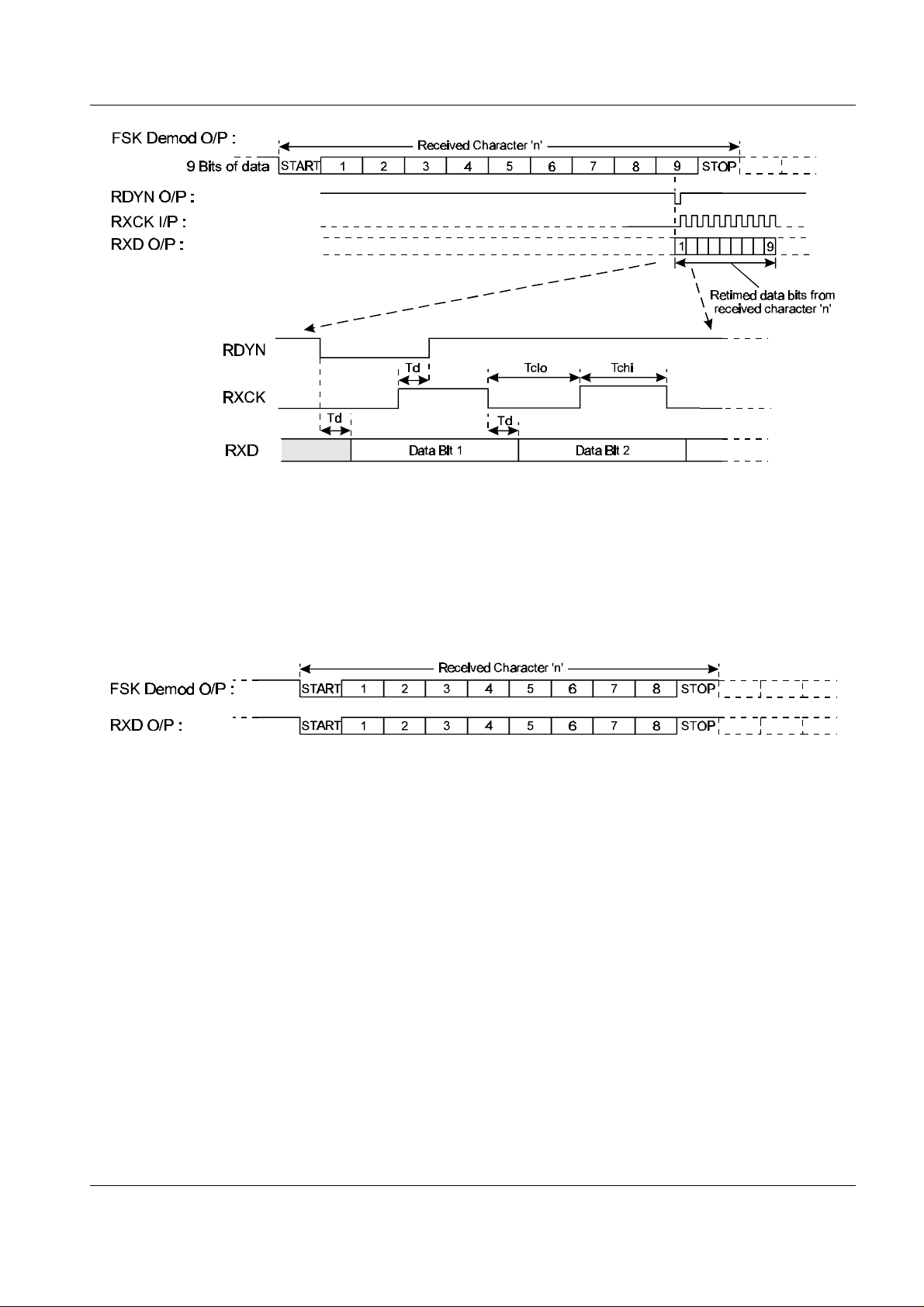
The Data Retiming block, when enabled in receive mode, extracts the first 9 bits of each character following
the start bit from the received asynchronous data stream, and presents them to the
µC under the control of
strobe pulses applied to the CLK input. The timing of these pulses is not critical and they may easily be
generated by a simple software loop. This facility removes the need for a UART in the
µC without incurring an
excessive software overhead.
The receive retiming block consists of two 9-bit shift registers, the input of the first is connected to the output
of the FSK demodulator and the output of the second is connected to the RXD pin. The first register is clocked
by an internally generated signal that stores the 9 received bits following the timing reference of a high to low
transition at the output of the FSK demodulator. When the 9th bit is clocked into the first register these 9 bits
are transferred to the second register, a new stop-start search is initiated and the CLK input is sampled. If the
CLK input is low at this time the RDYN pin is pulled low and the first received bit is output on the RXD pin. The
CLK pin should then be pulsed high 9 times, the first 8 high to low transitions will be used by the device to
clock out the bits in the second register. The RDYN output is cleared the first time the CLK input goes high. At
the end of the 9th pulse the RXD pin will be connected to the FSK demodulator output.
So to use the Data Retiming function, the CLK input should be kept low until the RDYN output goes low; if the
Data Retiming function is not required the CLK input should be kept high at all times.
The only restrictions on the timing of the CLK waveform are those shown in Figure 6a and the need to
complete the transfer of all nine bits into the
µC within the time of a complete character at 1200bits/sec.
1997 Consumer Microcircuits Limited 9 D/614/4
Page 10
Bell 202 Compatible Modem FX614
Td = Internal FX614 delay; max 1µs Tchi = CLK high time; min 1µs Tclo = CLK low time; min 1µs
Figure 6a FSK Operation with Rx Data Retiming
Note that, if enabled, the Data Retiming block may interpret speech or other signals as random characters.
If the Data Retiming facility is not required, the CLK input to the FX614 should be kept high at all times. The
asynchronous data from the FSK Demodulator will then be connected directly to the RXD output pin, and the
RDYN output will not be activated by the FSK signal. This case is illustrated by the example in Figure 6b.
Figure 6b FSK Operation without Rx Data Retiming (CLK always high)
1.5.9 Tx Data Retiming
The Data Retiming block, when enabled in 1200bits/sec transmit mode, requires the controlling
µC to load one
bit at a time into the device by a pulse applied to the CLK input. The timing of this pulse is not critical and it
may easily be generated by a simple software loop. This facility removes the need for a UART in the
µC
without incurring an excessive software overhead.
The Tx re-timing circuit consists of two 1-bit registers in series, the input of the first is connected to the TXD
pin and the output of the second feeds the FSK modulator. The second register is clocked by an internally
generated 1200Hz signal and when this occurs the CLK input is sampled. If the CLK input is high the TXD pin
directly controls the FSK modulator, if the CLK input is low the FSK modulator is controlled by the output of the
second register and the RDYN pin is pulled low. The RDYN output is reset by a high level on the CLK input
pin. A low to high change on the CLK input pin will latch the data from the TXD input pin into the first register
ready for transfer to the second register when the internal 1200Hz signal next occurs.
1997 Consumer Microcircuits Limited 10 D/614/4
Page 11
Bell 202 Compatible Modem FX614
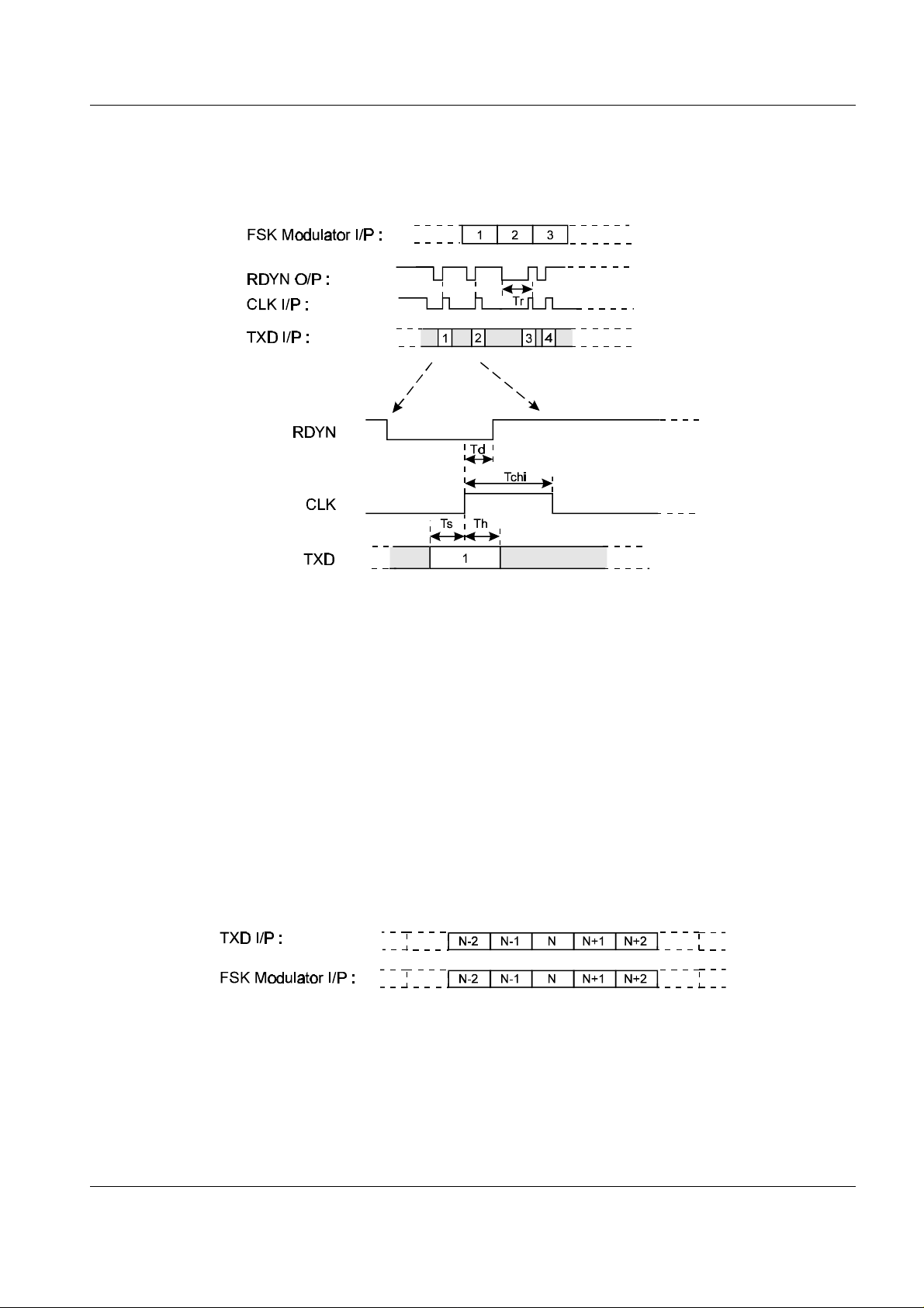
So to use the retiming option the CLK input should be held low until the RDYN output is pulled low. When the
RDYN pin goes low the next data bit should be applied at the TXD input and the CLK input pulled high and
then low within the time limits set out in Figure 6c.
Td = Internal FX614 delay; max 1µs
Tr = RDYN low to CLK going low; max 800
Tchi = CLK high time; min 1
µs Th = data hold time; min 1µs
µs Ts = data set up time; min 1µs
Figure 6c FSK Operation with Tx Data Retiming
To ensure synchronisation between the controlling device and the FX614 when entering Tx retiming mode the
TXD pin must be held at a constant logic level from when the CLK pin is first pulled low to the end of loading in
the second retimed bit. Similarly when exiting Tx retiming mode the TXD pin should be held at the same logic
level as the last retimed bit for at least 2 bit times after the CLK line is pulled high.
If the data retiming facility is not required, the CLK input to the FX614 should be kept high at all times. The
asynchronous data to the FSK modulator will then be connected directly to the TXD input pin. This is
illustrated in Figure 6d and will also be the case when transmitting 5bits/sec or 150bits/sec data which have no
retime option.
Figure 6d FSK Operation without Tx Data Retiming (CLK always high)
1997 Consumer Microcircuits Limited 11 D/614/4
Page 12
Bell 202 Compatible Modem FX614
1.6 Application Notes
1.6.1 Line Interface
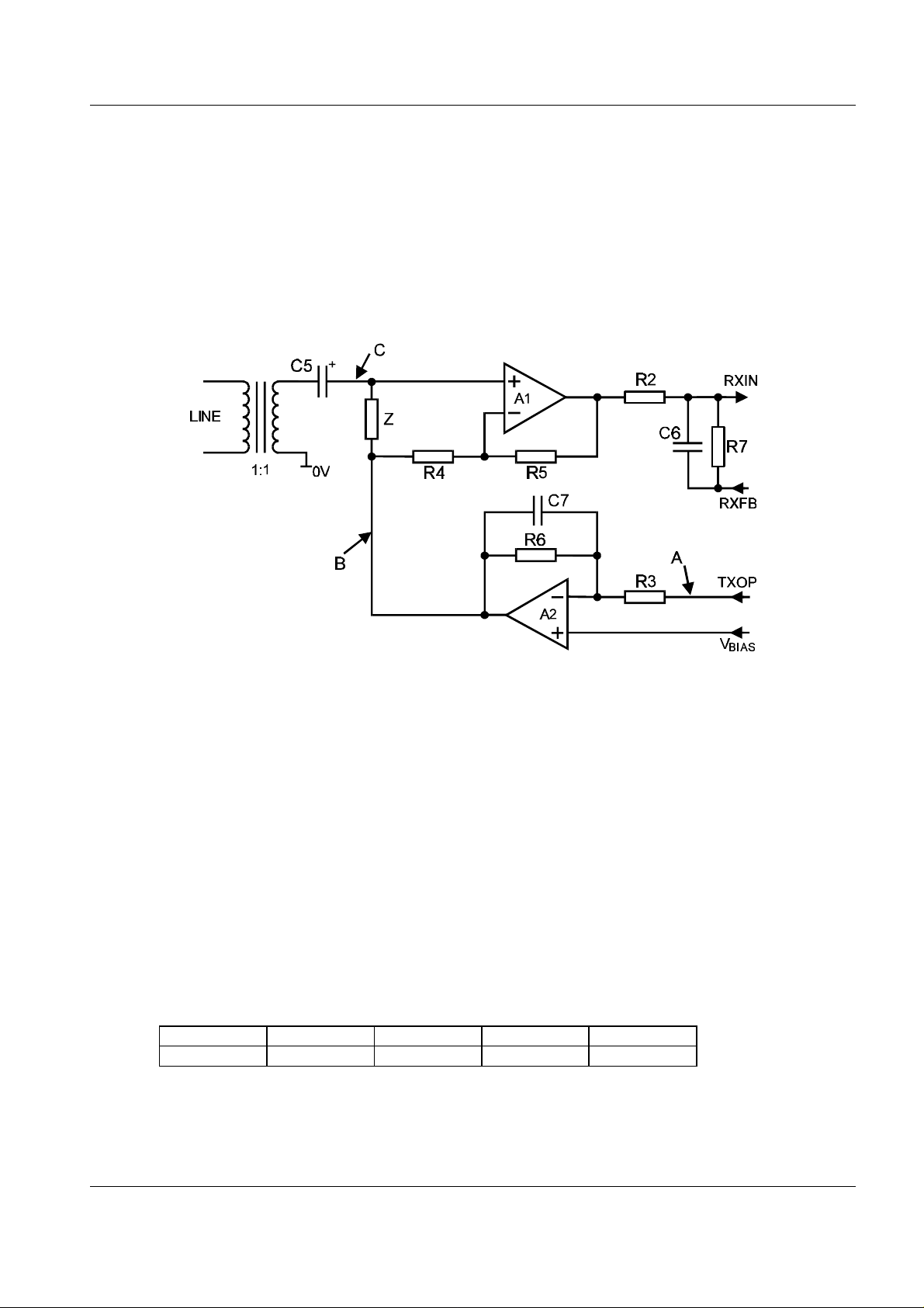
The signals on the telephone line are not suitable for direct connection to the FX614. A Line Interface circuit is
necessary to:
• Provide high voltage and dc isolation
• Attenuate the Tx signal present at the Rx input
• Provide the low impedance drive necessary for the line
• Filter the Tx and Rx signals
R2 See below C5
µF (±20%)
22
R3 See below C6 100pF
R4-R7
100k
Ω
Resistors
±1%, capacitors ±10% unless otherwise stated.
C7 330pF
Figure 7 Line Interface Circuit
Notes:
• The components 'Z' between points B and C should match the line impedance.
• Device A2 must be able to drive 'Z' and the line.
• R2: For optimum results R2 should be set so that the gain is V
5.0V, rising to 150k
Ω at V
= 3.3V.
DD
/5.0, i.e. R2 = 100kΩ at VDD =
DD
• R3: The levels in dB (relative to a 775mV rms signal) at 'A', 'B' and 'C' in the line interface circuit are:
Level at 'A' = 20Log(V
"
'B' = 'A' + 20Log(100k
DD/5)
Ω/R3)
" 'C' = 'B' - 6
Example:
DD 'A' R3 'B' 'C'
V
3.3V -3.6dB
5.0V 0dB
100k
150k
Ω
Ω
-3.6dB -9.6dB
-3.5dB -9.5dB
1997 Consumer Microcircuits Limited 12 D/614/4
Page 13

Bell 202 Compatible Modem FX614
1.7 Performance Specification
1.7.1 Electrical Performance
Absolute Maximum Ratings
Exceeding these maximum ratings can result in damage to the device.
Min. Max. Units
Supply (VDD - VSS) -0.3 7.0 V
Voltage on any pin to V
Current into or out of V
SS
DD
and V
pins -30 +30 mA
SS
Current into or out of any other pin -20 +20 mA
D4 Package Min. Max. Units
Total Allowable Power Dissipation at Tamb = 25°C 800 mW
... Derating 13 mW/°C
Storage Temperature -55 +125 °C
Operating Temperature -40 +85 °C
P3 Package Min. Max. Units
Total Allowable Power Dissipation at Tamb = 25°C 800 mW
... Derating 13 mW/°C
Storage Temperature -55 +125 °C
Operating Temperature -40 +85 °C
-0.3 V
+ 0.3 V
DD
Operating Limits
Correct operation of the device outside these limits is not implied.
Notes Min. Max. Units
Supply (VDD - VSS) 3.0 5.5 V
Operating Temperature -40 +85 °C
Xtal Frequency 1 3.575965 3.583125 MHz
Notes: 1. A Xtal/Clock frequency of 3.5795MHz ±0.1% is required for correct FSK operation.
1997 Consumer Microcircuits Limited 13 D/614/4
Page 14

Bell 202 Compatible Modem FX614
Operating Characteristics
For the following conditions unless otherwise specified:
= 3.0V at Tamb = 25°C and V
V
DD
Xtal Frequency = 3.579545MHz
= 3.3V to 5.5V at Tamb = -40 to +85°C,
DD
± 0.1%
0dBV corresponds to 1.0Vrms
0dBm corresponds to 775mVrms into 600
Ω.
Notes Min. Typ. Max. Units
DC Parameters
IDD (M0 = '1', M1 = '1') 1, 2 - 1.0 -
(M0 or M1 = '0') at VDD = 3.0V 1 - 1.0 1.25 mA
I
DD
(M0 or M1 = '0') at VDD= 5.0V 1 - 1.7 2.5 mA
I
DD
Logic '1' Input Level 70% - - V
Logic '0' Input Level - - 30% V
Logic Input Leakage Current (Vin = 0 to VDD),
-1.0 - +1.0
µA
DD
DD
µA
Excluding XTAL/CLOCK Input
V
Output Logic '1' Level (l
Output Logic '0' Level (l
= 360µA)
OH
= 360µA)
OL
RDYN O/P 'off' State Current (Vout = V
) - - 1.0
DD
-0.4 - - V
DD
- - 0.4 V
µA
FSK Demodulator
Bit Rate 0 1200 1212 Baud
Mark (Logical '1') Frequency 1188 1200 1212 Hz
Space (Logical '0') Frequency 2178 2200 2222 Hz
Valid Input Level Range 3 -40.0 - -8.0 dBV
Maximum Twist (Mark Level wrt Space Level) ±6.0 - - dB
Acceptable Signal to Noise Ratio 4 20.0 - - dB
Level Detector 'On' Threshold Level 3 - - -40.0 dBV
Level Detector 'Off' to 'On' Time (Figure 4 Teon) - - 25.0 ms
Level Detector 'On' to 'Off' Time (Figure 4 Teoff) 8.0 - - ms
FSK Retiming
Acceptable Rx Data Rate 1188 1200 1212 Baud
Tx Data Rate 1194 - 1206 Baud
FSK Modulator
TXOP Level 5 -1.0 0 +1.0 dB
Twist (Mark Level wrt Space Level) -2.0 0 +2.0 dB
Tx 1200bits/sec (M1 = '0', M0 = '1').
Bit Rate 0 1200 1212 Baud
Mark (Logical '1') Frequency 1197 - 1203 Hz
Space (Logical '0') Frequency 2196 - 2204 Hz
Tx 150bits/sec (M1 = '0', M0 = '0')
Bit Rate 0 150 152 Baud
Mark (Logical '1') Frequency 385 - 389 Hz
Mark (Logical '0') Frequency 485 - 489 Hz
1997 Consumer Microcircuits Limited 14 D/614/4
Page 15

Bell 202 Compatible Modem FX614
Notes Min. Typ. Max. Units
Tx 5bits/sec (M1 = '1', M0 = '0').
Bit Rate 0 5.0 5.1 Baud
Mark (Logical '1') Frequency 385 - 389 Hz
Space (Logical '0') Frequency 6 - 0 - Hz
Data and Mode Timing
Rx Data Delay (RXIN to RXD) 9 - 2.55 - ms
Tx Data Delay (TXD to TXOP) 9 - 0.1 - ms
Mode ZP to Tx or Rx 10 - - 20 ms
Mode Tx1200 to Rx1200 10 - - 4.0 ms
Mode Rx1200 to Tx1200 10 - - 0.2 ms
Input Amplifier
Impedance (RXIN Pin) 7 10.0 - -
M
Ω
Voltage Gain 7 - 500 - V/V
XTAL/CLOCK Input
'High' Pulse Width 8 100 - - ns
'Low' Pulse Width 8 100 - - ns
Notes: 1. At 25°C, not including any current drawn from the FX614 pins by external circuitry other than
X1, C1 and C2.
2. TXD, RXEQ and CLK inputs at V
3. Measured at the Rx Input Amplifier output (pin RXFB) for 1200Hz and V
The internal threshold levels are proportional to V
, M0 and M1 inputs at VDD.
SS
. To cater for other supply voltages or
DD
= 5.0V.
DD
different signal level ranges the voltage gain of the Rx Input Amplifier should be adjusted by
selecting the appropriate external components as described in section 1.6.1
4. Flat noise in 200 - 3200Hz band.
5. Relative to 775mVrms at V
6. TXOP held at approximately V
= 5.0V for load resistances greater than 40kΩ.
DD
/2.
DD
7. Open loop, small signal low frequency measurements.
8. Timing for an external input to the XTAL/CLOCK pin.
9. Assuming data retiming is not enabled.
10. Delay from mode change to reliable data at TXOP or RXD pins.
1997 Consumer Microcircuits Limited 15 D/614/4
Page 16
Bell 202 Compatible Modem FX614
1.7.2 Packaging
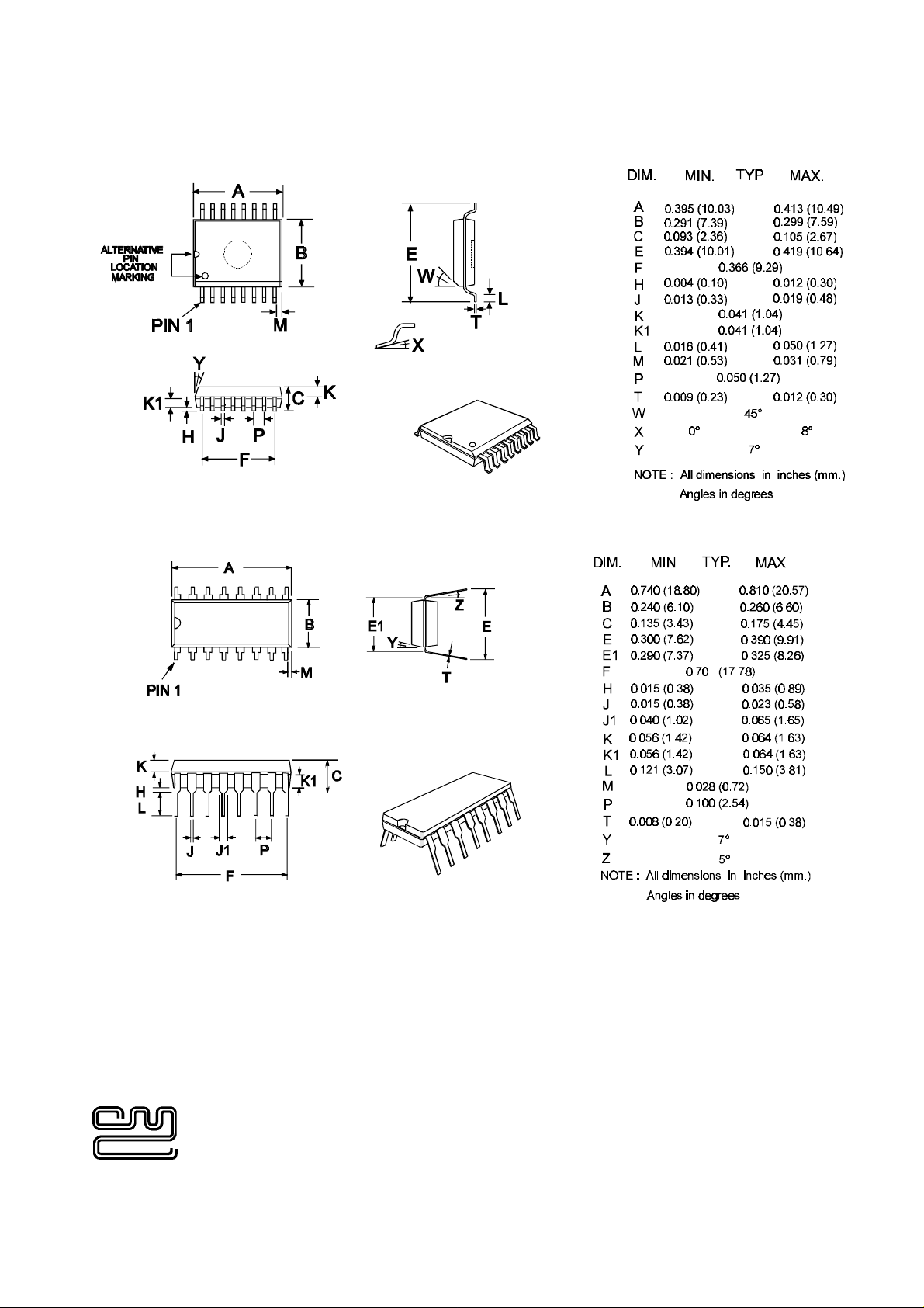
Figure 8 16-pin SOIC (D4) Mechanical Outline: Order as part no. FX614D4
Figure 9 16-pin DIL (P3) Mechanical Outline: Order as part no. FX614P3
Handling precautions: This product includes input protection, however, precautions should be taken to prevent
device damage from electro-static discharge. CML does not assume any responsibility for the use of any circuitry
described. No IPR or circuit patent licences are implied. CML reserves the right at any time without notice to
change the said circuitry and this product specification. CML has a policy of testing every product shipped using
calibrated test equipment to ensure compliance with this product specification. Specific testing of all circuit
parameters is not necessarily performed.
CONSUMER MICROCIRCUITS LIMITED
1 WHEATON ROAD Telephone: +44 1376 513833
WITHAM - ESSEX Telefax: +44 1376 518247
CM8 3TD - ENGLAND e-mail: [email protected]
http://www.cmlmicro.co.uk
Page 17

CML Microcircuits
COMMUNICATION SEMICONDUCTORS
CML Product Data
In the process of creating a more global image, the three standard product semiconductor
companies of CML Microsystems Plc (Consumer Microcircuits Limited (UK), MX-COM, Inc
(USA) and CML Microcircuits (Singapore) Pte Ltd) have undergone name changes and, whilst
maintaining their separate new names (CML Microcircuits (UK) Ltd, CML Microcircuits (USA)
Inc and CML Microcircuits (Singapore) Pte Ltd), now operate under the single title CML Micro-
circuits.
These companies are all 100% owned operating companies of the CML Microsystems Plc
Group and these changes are purely changes of name and do not change any underlying legal
entities and hence will have no effect on any agreements or contacts currently in force.
CML Microcircuits Product Prefix Codes
Until the latter part of 1996, the differentiator between products manufactured and sold from
MXCOM, Inc. and Consumer Microcircuits Limited were denoted by the prefixes MX and FX
respectively. These products use the same silicon etc. and today still carry the same prefixes.
In the latter part of 1996, both companies adopted the common prefix: CMX.
This notification is relevant product information to which it is attached.
Company contact information is as below:
CML Microcircuits
(UK) Ltd
COMMUNICATION SEMICONDUCTORS
Oval Park, Langford, Maldon,
Essex, CM9 6WG, England
T el: +44 (0)1621 875500
Fax: +44 (0)1621 875600
[email protected]
www.cmlmicro.com
COMMUNICATION SEMICONDUCTORS
4800 Bethania Station Road,
Winston-Salem, NC 27105, USA
Tel: +1 336 744 5050,
Fax: +1 336 744 5054
[email protected]
www.cmlmicro.com
CML Microcircuits
(USA) Inc.
0800 638 5577
COMMUNICATION SEMICONDUCTORS
No 2 Kallang Pudding Road, 09-05/
06 Mactech Industrial Building,
Singapore 349307
T el: +65 7450426
Fax: +65 7452917
[email protected]
www.cmlmicro.com
CML Microcircuits
(Singapore)Pte Ltd
D/CML (D)/1 February 2002
 Loading...