

Page 1
Publication D/613/3 December 1995
CML Semiconductor Products
FX613
PRODUCT INFORMATION
The FX613 is a wide-band, ‘N-Tone’, non-predictive
tone decoder to measure telephone system call progress
tones in PABX, Pay/Feature-Phone, Fax and Modem
systems.
Adhering to Must/Must-Not Decode limits and able to
measure inband frequencies in outband modulation, this
decoder measures the frequency of input signals in the
range 300Hz to 2,150Hz; the result of each
measurement is presented to a system µProcessor, as a
6-bit serial word.
The decode frequency range, which covers the
World's call progress application spectrum, is processed
internally as two bands: LO = 300Hz to 660Hz and HI =
900Hz to 2150Hz. Frequency measurement is achieved
by counting the number of cycles in a set time period
(LO = 39.47ms or HI = 13.16ms). Bad signal/level quality
or NOTONE results in a count-abort, timing-reset and no
output from the decoder.
Current frequency information is output for the
µProcessor using a Serial Data, Clock and Interrupt
interface.
Data from the FX613 should be processed by a
µProcessor whose algorithms are able to recognize the
frequency, sequence and/or cadence of input signals as
national call progress information; e.g.: ‘Dial’, ‘Busy’,
‘Number-Unobtainable’, ‘Ringing’ and automatic tones
employed by Fax, Modem systems. Software can be
simply configured to reject speech frequencies.
Due to its ‘N-Tone’, non-predictive decoding capability,
units employing the FX613 can be redeployed under a
new national standard by a simple software amendment.
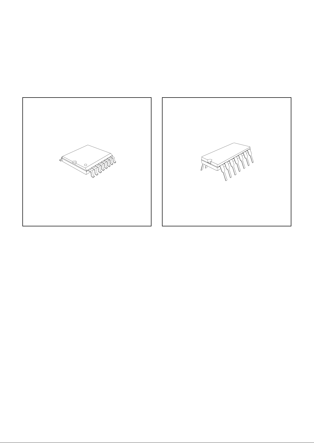
Available in 16-pin plastic S.O.I.C. SMD and 14-pin
plastic DIL packages, this low-cost, mixed analogue/digital
microcircuit has a typical power requirement of less than
1mA at 3 volts and utilizes a telecom-system clock input
of 3.579545MHz to maintain frequency accuracy.
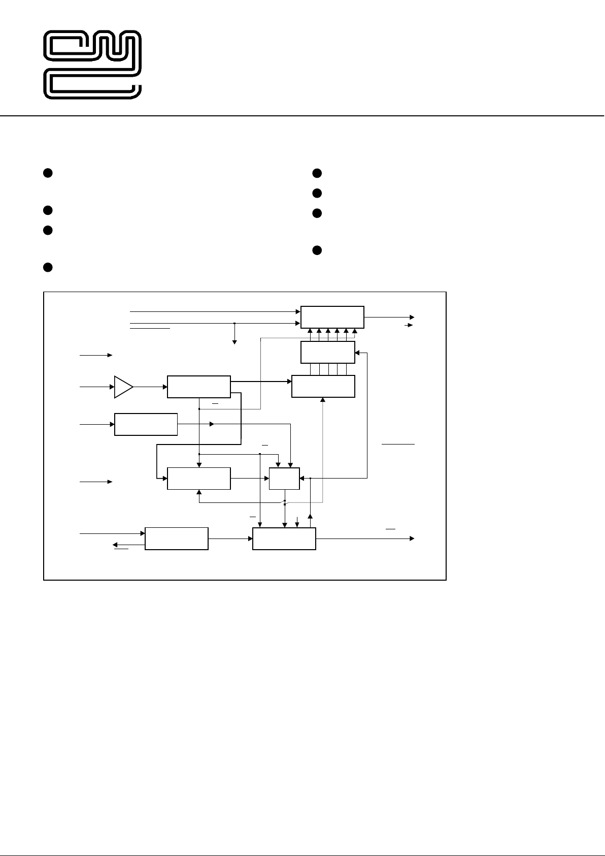
Fig.1 Functional Block Diagram
Brief Description
Universal Call Progress Decoder
CLOCK
GENERATOR
LOGIC
SERIAL CLOCK
SIGNAL IN
V
SS
V
DD
V
BIAS
LEVEL IN
DATA OUT
XTAL/CLOCK
3.579545MHz
TIME
CS
CS
GOOD/BAD
TIME
RESET
RESET
RESET
COUNT
DECODE
ON / OFF
f
f/4
f/4
IRQ
XTAL
CHIP SELECT
HI/LO
HI/LO
HI / LO BAND
FREQUENCY
COUNTER
LATCH
SERIAL OUTPUT
PORT (6-BITS)
TIMER
LO = 39.4ms
HI = 13.16ms
012345
SIGNAL QUALITY
ASSESSOR
LEVEL
DETECTOR
FILTER &
BAND SELECTOR
FX613
Features
Covers Worldwide Call Progress
Frequencies (300Hz to 2,150Hz)
3 Volt <1mA Requirement
Decodes Single or Modulated
T ones
Analogue In/Serial Data Out
Speech Discrimination Ability
µProcessor Compatible Outputs
Telephone/Telecoms, Radio and
Fax/Modem Applications
Mixed Analogue/Digital
Technology
Page 2
2
FX613DW
1
2
3
4
5
6
7
8
9
10
11
12
13
14
15
16
FX613P
1
2
3
4
5
6
7
8
9
10
11
12
13
14
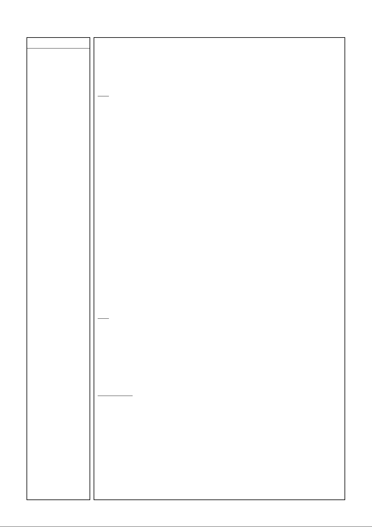
Pin Number Function
Xtal/Clock: The input to the on-chip clock oscillator inverter. A 3.579545MHz Xtal or
externally derived telephone system clock (f
XTAL
) should be connected here.
Note - The operation of the FX613 without a suitable Xtal/Clock input may cause
device damage.
Xtal: The output of the on-chip clock oscillator inverter. See Figure 2.
No internal connection.
V
BIAS
: The internal circuitry bias line, held at VDD/2 this pin must be decoupled to VSS.
Level In: The input for level discrimination. This input is internally biased to V
BIAS
,
signals must be a.c. coupled. The audio signal must be fed to both this pin and the
Signal In pin. Correct level detection determines the operation of this device (see
Principles of Decoder Operation), however to disregard the amplitude of the input
levels the FX613 may be permanently enabled by pulling this pin to VDD and disabled
by pulling to VSS.
Signal In: The input for frequency discrimination and decoding. This input is internally
biased to V
BIAS
, signals must be a.c. coupled. The audio signal must be fed to both this
pin and the Level In pin.
No internal connection.
VSS: Negative supply rail. Signal ground.
No internal connection.
No internal connection.
IRQ: This Interrupt Request output from the FX613 is ‘wire-OR able’ allowing the
interrupt outputs of other peripherals to be combined and connected to the Interrupt
input of a µProcessor. This input has a low-impedance pulldown to V
SS
when active and
a high-impedance when inactive. An interrupt is produced on completion of a HI or LO
frequency measurement.
Serial Clock: The serial clock from the µProcessor. Data Out is clocked into the
µProcessor on the rising edge of the Serial Clock. See Data-Read Timing diagram.
Chip Select: A logic “0” at this input will select this device.
Data Out: The serial data output. Under the control of the Chip Select and Serial
Clock inputs, data should be read from this output in 6-bit blocks MSB (Bit-5) first.
If 8 serial clock pulses are applied, two additional logic “0s” will be output after Bit-0.
No internal connection.
VDD: Positive supply rail. A single, stable supply is required. Levels and voltages within
the FX613 are dependent upon this supply. This pin should be decoupled to VSS by a
capacitor located close to the FX613 pins.
Page 3
3
Application Information
V
DD
V
SS
V
SS
V
SS
C
1
C
4
C
2
C
3
R
1
V
BIAS
1
2
3
4
5
6
7
8
14
15
16
13
12
11
10
9
FX613DW
SERIAL CLOCK INPUT
DAT A OUT
LEVEL IN
SIGNAL IN
AUDIO SIGNAL
XTAL/CLOCK
V
DD
XTAL
IRQ
CHIP SELECT
C
5
C
6
R
2
X
1
1
2
V
SS
0
0
200 400 600 800 1000 1200 1400 1600 1800 2000 2200
-50
-40
-30
-20
-10
V
DD
775mVrms
Must
Decode
Level (dB)
Frequency (Hz)
Must-Not
Decode
Low Band
(LO)
High Band
(HI)
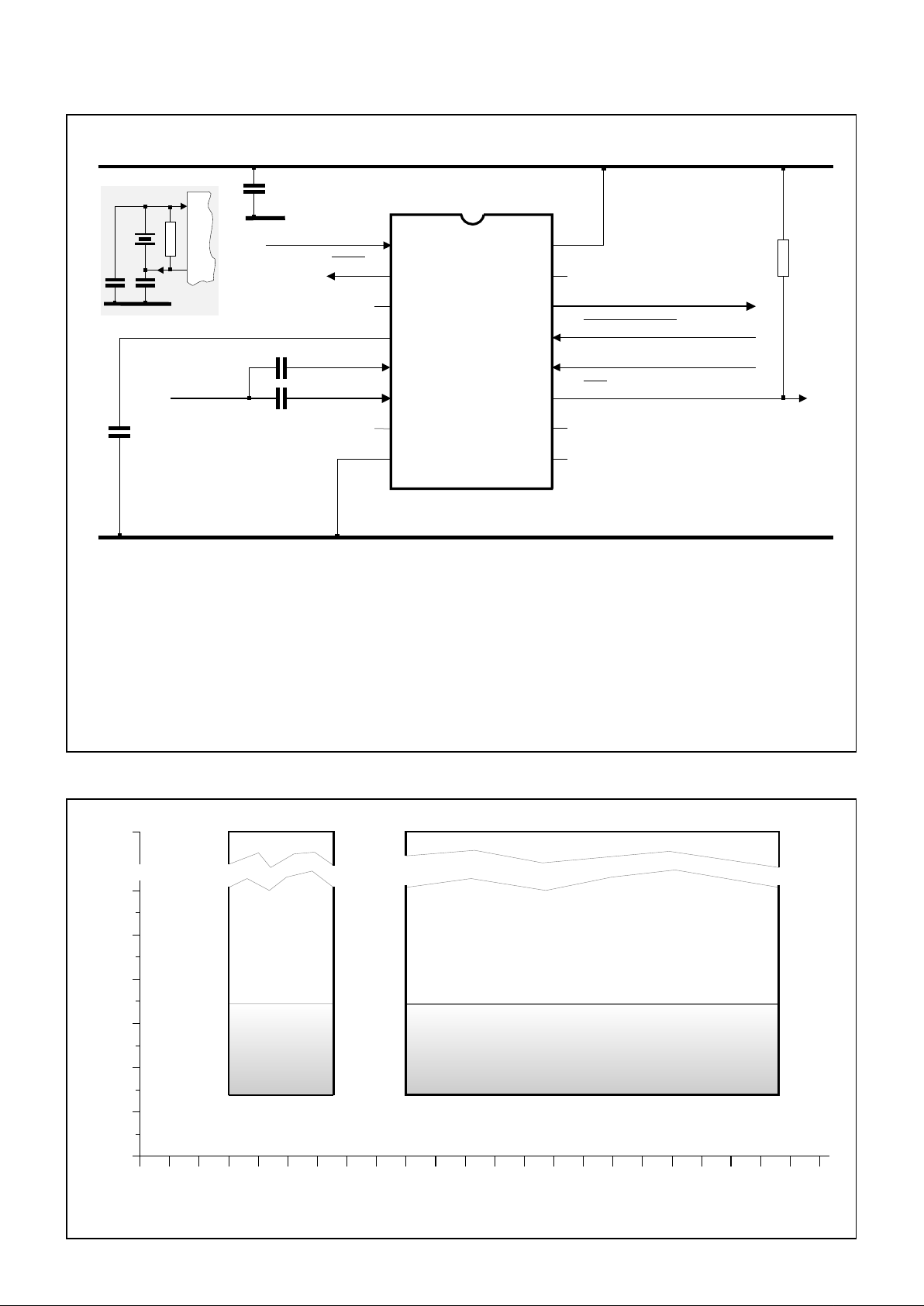
Fig.3 HI/LO Decode Bands
Fig.2 External Component Connections
Component Value
R
1
22.0kΩ
R
2
1.0MΩ
C
1
0.01µF
C
2
0.1µF
C
3
1.0µF
C
4
1.0µF
C
5
33.0pF
C
6
33.0pF
X
1
3.579545MHz
Tolerances: C = ± 20% R = ± 10%
Notes
(1) The Xtal/Clock input may be driven from the host telephone
system's 3.579545MHz clock; if a Xtal drive is required, the
configuration shown INSET is recommended.
(2) The audio signal should be input to both Signal In and Level In pins
via separate coupling capacitors. If it is wished to operate the
device with disregard to on-chip level thresholds and permanently
enable the FX613, the Level In pin should be held at VDD.
To disable the FX613 the Level In pin should be held at VSS. Level
thresholds are preset internally.
Page 4
4
Application Information ......
Principles of Decoder Operation
Level Detection
As level and frequency discrimination operations
take place in parallel the audio signal should, under
normal circumstances, be input to both Signal In and
Level In pins via coupling capacitors.
If the input signal level (Level In) is outside the
preset ‘Must/Must Not Decode’ thresholds
(Specification Page), the Universal Call Progress
Decoder will be disabled.
If it is wished to disregard signal input
levels
at the
Level In pin and attempt to decode under all
conditions, the decoder may be permanently enabled
by holding the Level In pin at VDD.
The device can disabled by pulling Level In to VSS.
NOTONE Recognition
The NOTONE condition can be recognized using
µProcessor software timing as below.
a. Set the µP timer period to a period greater than
the relevant frequency-band measurement
period (13.16ms or 39.47ms).
b. Each ‘Tone Measurement Complete’ interrupt
from the FX613 must reset the µP timer.
c. With NOTONE or white noise at the decoder input,
the FX613 on-chip timer will be continually reset.
ii No ‘Tone Measurement Complete’ interrupt
will occur - the µP timer will run.
ii The µP Timer time-out can be considered as
a NOTONE indication.
Frequency Band Discrimination
The input signal is amplified by a self-biased (zerocrossing) inverting amplifier and then ‘filtered’ to
remove high-frequency noise and jitter.
High (HI) and Low (LO) counters are employed to
determine the input frequency band (HI = 900Hz to
2150Hz, LO = 300Hz to 660Hz).
If the input frequency is in the LO Band, the device
will operate as a LO Band decoder and will remain so
until a HI frequency signal is detected. If the input
frequency is in the HI Band, the device will operate as
a HI Band decoder and will remain so until a LO
frequency signal is detected.
Frequency band monitoring is continuous with the
band selection taking place every 9.8ms. It will
therefore take 9.8ms from Power-Up to set up the
initial correct decode frequency band.
On-Chip Timer Operation
For frequency measurement, the FX613 counts
the number of input cycles in a fixed time period. This
fixed period, measured by the continuous on-chip
timer, is set to 13.16ms for HI Band inputs and
39.47ms for LO Band inputs.
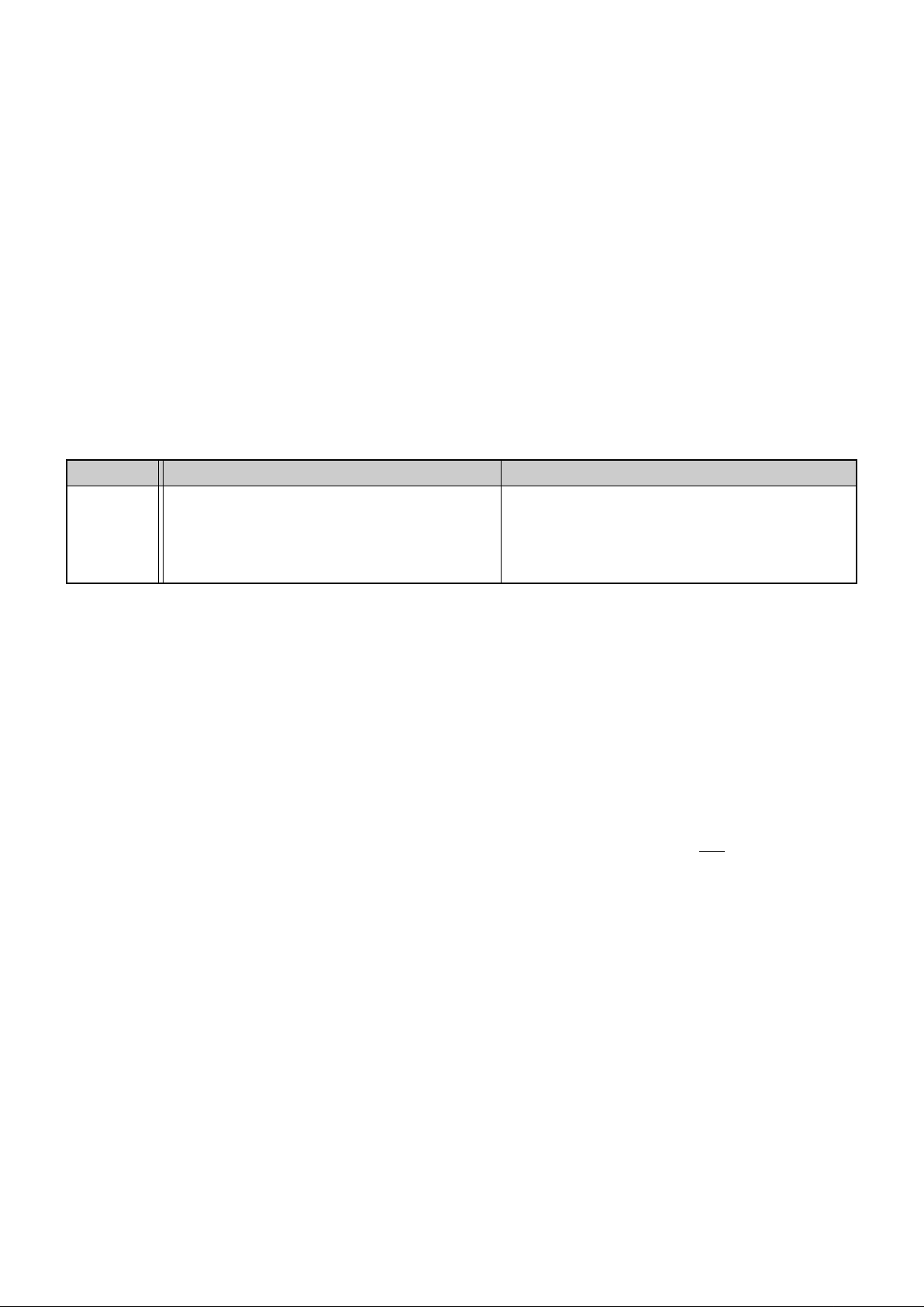
Level In Timer IRQ Data Out
In Limits Running Enabled Enabled
Out of Limits Reset Disabled Disabled (frozen to previous bit-5 level
V
DD
Running/Reset Enabled/Disabled Enabled (dependent upon Quality measurement)
V
SS
Reset Disabled Disabled (frozen to previous bit-5 level)
On-Chip Timer Operation ......
When the timer expires the following actions take
place:
a. A HI or LO (“1” or “0”) band indication bit is
latched into Bit-5 of the Serial Output Port.
b. The Frequency Counter count of 5-bits is latched
into the Serial Output Port (Bit-4 [MSB] to Bit-0).
The Serial Output Port Contains 6-bits, if 8 Serial
Clock edges are employed, two extra “0s”, which
should be ignored, will be output last.
c. An interrupt is generated (IRQ) to the
µProcessor. The contents of the Serial Output
Port should be read before the next interrupt is
expected; if not data will be overwritten.
When the Chip Select input is set to “0” the
interrupt is reset.
The On-Chip Timer and Frequency Counter will be
reset in mid-count, and therefore unable to allow a
valid measurement, under the following conditions:
a. A change of decode frequency band.
b. Decoder disabled; signal input level out of
specification or Level Detect input set to VSS.
c. Signal Quality Assessment considered ‘Bad’.
d. Input signal frequency outside limits.
Page 5
5
Application Information ......
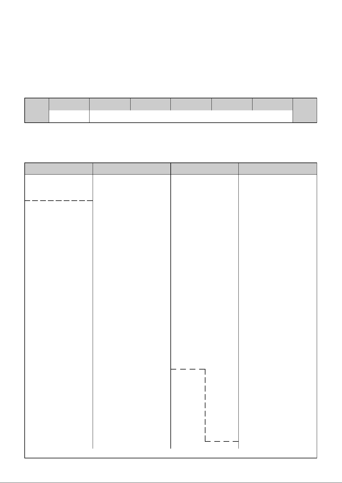
N = int (Frequency x Measurement Period)
Measurement Period = 39.47ms for Low Band (300Hz to 660Hz)
= 13.16ms for High Band (900Hz to 2150Hz)
Note: For input frequencies of between 661Hz and 899Hz the FX613 will give no reliable output.
Band Bit (5) MSB (4) (3) (2) (1) LSB (0)
HI-“1”/LO-“0” Bits 0 to 4 represent the measured frequency in the selected band
Bit 5
Output
First
Bits
0 to 4
=
N
When a ‘correct’ decode has been allowed and an interrupt generated, a 6-bit data word will be presented at the
Serial Output Port. This 6-bit word indicates the input frequency's band and value as described below.
As an example, the following binary-word presented at the Serial Output Port (1 1 0 1 1 0) will indicate a
frequency in the HI Band of between 1680Hz and 1740Hz (Bit-5 = “1” = HI, ‘N’ = 22).
LO Band HI Band N B5B4B3B2B1B0LO Band HI Band N B5B4B3B2B1B
0
280 840
11 H/L 01011 505 1515 19 H/L 1 0 0 1 1
285 855
11 510 1530 20 H/L 1 0 1 0 0
290 870
11 515 1545 20
295
885 11 520 1560 20
300 900 11 525 1575 20
305 915 12 H/L 01100 530 1590 20
310 930 12 535 1605 21 H/L 1 0 1 0 1
315 945 12 540 1620 21
320 960 12 545 1635 21
325 975 12 550 1650 21
330 990 13 H/L 01101 555 1665 21
335 1005 13 560 1680 22 H/L 1 0 1 1 0
340 1020 13 565 1695 22
345 1035 13 570 1710 22
350 1050 13 575 1725 22
355 1065 14 H/L 01110 580 1740 22
360 1080 14 585 1755 23 H/L 1 0 1 1 1
365 1095 14 590 1770 23
370 1110 14 595 1785 23
375 1125 14 600 1800 23
380 1140 14 605 1815 23
385 1155 15 H/L 01111 610 1830 24 H/L 1 1 0 0 0
390 1170 15 615 1845 24
395 1185 15 620 1860 24
400 1200 15 625 1875 24
405 1215 15 630 1890 24
410 1230 16 H/L 10000 635 1905 25 H/L 1 1 0 0 1
415 1245 16 640 1920 25
420 1260 16 645 1935 25
425 1275 16 650 1950 25
430 1290 16 655 1965 25
435 1305 17 H/L 10001 660 1980 26 H/L 1 1 0 1 0
440 1320 17
665
1995 26
445 1335 17
670
2010 26
450 1350 17
675
2025 26
455 1365 17
680
2040 26
460 1380 18 H/L 10010
685
2055 27 H/L 1 1 0 1 1
465 1395 18
690
2070 27
470 1410 18
695
2085 27
475 1425 18
700
2100 27
480 1440 18
705
2115 27
485 1455 19 H/L 10011
710
2130 28 H/L 1 1 1 0 0
490 1470 19
715
2145 28
495 1485 19
720
2160 28
500 1500 19
725 2175
28
Table 1 Decode Frequency Data
Page 6
6
Application Information ......
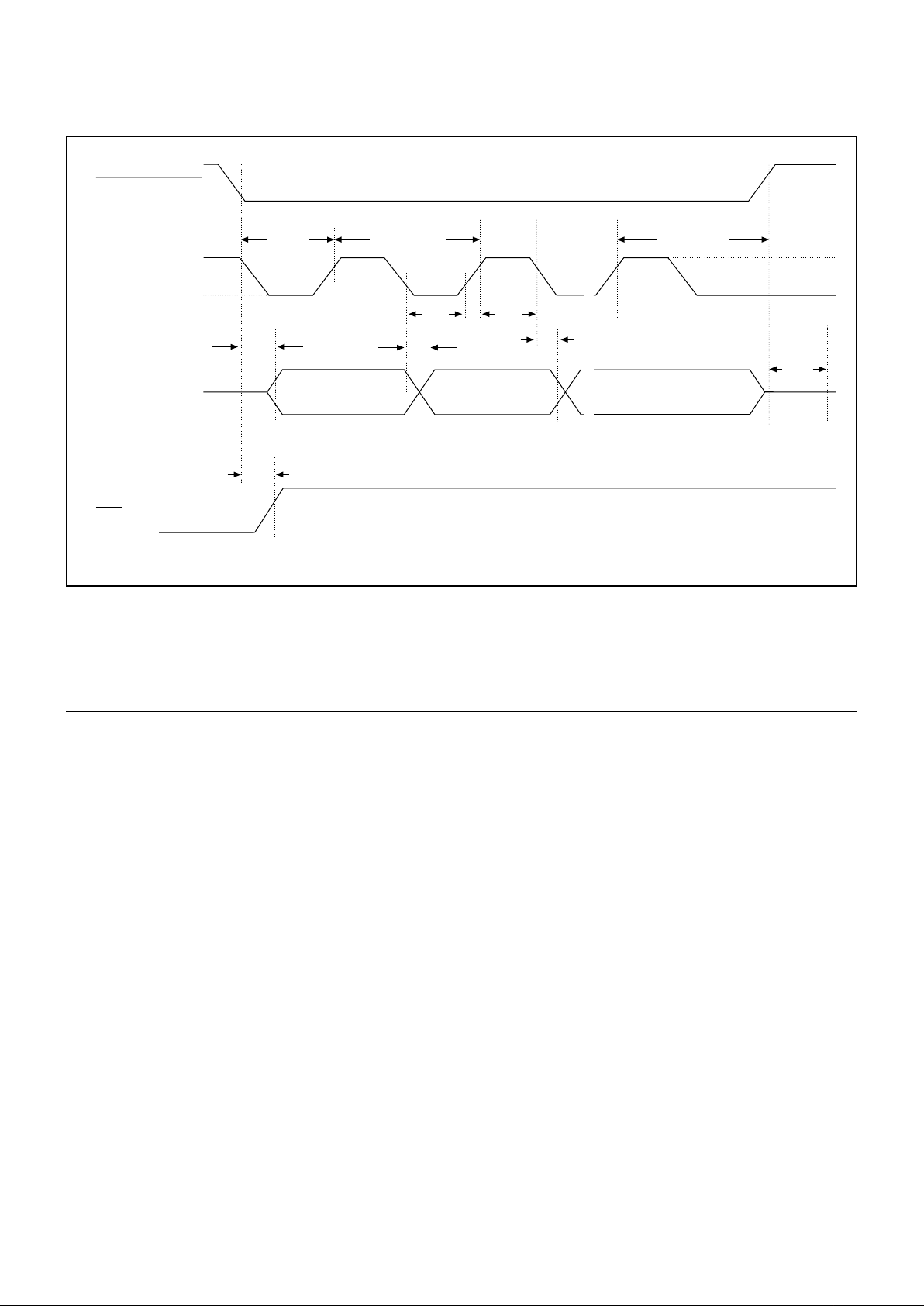
Decoder Timing
CHIP SELECT
SERIAL CLOCK
DATA OUT
BIT 5
BIT 4
BIT 0
TRI-STATE
t
CSE
t
DE
t
CDS
t
HIZ
t
PWL
t
PWH
t
DH
t
IR
t
CSH
t
CYC
IRQ
Fig.4 Data-Read Timing
Decoder Timing Characteristics
With reference to Figure 4,
Data-Read Timing
.
Characteristics Min. Typ. Max. Unit
t
PWH
Serial Clock “High” Pulse Width 250 - - ns
t
PWL
Serial Clock “Low” Pulse Width 250 - - ns
t
CYC
Serial Clock-Cycle Time 600 - - ns
t
CSE
Chip Select Low to Clock “High” Edge 450 - - ns
t
CSH
Last Clock “High” Edge to CS “High” 600 - - ns
t
DH
Data Out Hold Time 0 - - ns
t
CDS
Clock Edge to Data Out Set Time - - 200 ns
t
IR
Interrupt (IRQ) Reset Time - - 200 ns
t
DE
Chip Select “Low” to Data Enable - - 200 ns
t
HIZ
Chip Select “High” to Output Tri-State - - 1000 ns
Notes
1 Data is output bit 5 first. Bit 5 can be clocked into the µProcessor by the first Serial Clock rising edge.
If 8 Serial Clock pulses are employed the last 2 data-bits will be “0” and should be ignored by the
software.
2 Chip Select should be used to react to Interrupts and then returned to a logic “1”.
If Chip Select stays low there will be no further Interrupts and no Data Output update.
Page 7

7
Specification
Absolute Maximum Ratings
Exceeding the maximum rating can result in device damage. Operation of the device outside the operating limits is
not implied.
Supply voltage -0.3 to 7.0V
Input voltage at any pin (ref V
SS
= 0V) -0.3 to (V
DD
+ 0.3V)
Sink/source current (supply pins) +/- 30mA
(other pins) +/- 20mA
Total device dissipation @ T
AMB
25°C 800mW Max.
Derating 10mW/°C
Storage temperature range: FX613DW/P -40°C to +85°C (plastic)
Operating Limits ...... Min. Max. Unit
Supply Voltage (VDD) 3.0 5.5 V at 25°C
Operating Temperature ...... -40 +85 °C
All device characteristics are measured under the following conditions unless otherwise specified:
V
DD
= 3.3V, T
OP
= -40 to +85 °C. Audio Level 0dB ref: = 775mVrms. Xtal/Clock Frequency = 3.579545MHz
Characteristics See Note Min. Typ. Max. Unit
Static Values
Supply Current - 0.3 1.0 mA
Input Logic “1” 70.0 - 100 % V
DD
Input Logic “0” 0 - 30.0 % V
DD
Output Logic “1” 1 90.0 - 100 % V
DD
Output Logic “0” 1 - - 10.0 % V
DD
Impedances
Chip Select and Serial Clock Input 10.0 - - MΩ
Signal Input - 50.0 - kΩ
Level Input - 210 - kΩ
IRQ Output (logic “0”) - - 500 Ω
Data Output (logic “0”) - 500 - Ω
(Logic “1”) - - 2.5 kΩ
Dynamic Values
On-Chip Xtal Oscillator
R
IN
10.0 - - MΩ
R
OUT
- 230 825 kΩ
DC Voltage Gain 25.0 42.0 - V/V
Bandwidth at Unity Gain 5.0 11.0 - MHz
Single Tone Operation
Must-Decode Input Level 2 -25.2 - - dB
Must-Not Decode Input Level 2 - - -46.0 dB
LO Band Frequency Range 4 300 660 Hz
HI Band Frequency Range 4 900 2150 Hz
Frequency Resolution (Table 1)
LO Band - - 25.0 Hz
HI Band - - 75.0 Hz
Input Signal/White-Noise Ratio (HI & LO Bands) - 18.0 - dB
Interrupt Rate (LO Band) 3 19.0 - - /sec
(HI Band) 3 57.0 - - /sec
False Decodes Due to Noise 6 - 1.0 - /2 secs
Outband modulation level limits
for correct decode (fIN = 340Hz to 620Hz) 5 - - 10.0 %
Notes
1. Into a high-impedance load (>1.0MΩ).
2. Must decode signal above -25.2dB; Must Not decode signal below -46.0dB.
If a supply other than 3.3 volts is used, levels will change pro-rata.
3. Under ‘Pure Tone’ input conditions.
4. For input frequencies of between 661Hz and 899Hz the FX613 will provide no reliable output.
5. With an amplitude modulating frequency of between 16.0Hz and 100Hz.
6. Test noise input = 5.0kHz at 100mVrms
Page 8
NOT TO SCALE
Max. Body Length 20.57mm
Max. Body Width 6.60mm
Handling Precautions
The FX613 is a CMOS LSI circuit which includes input
protection. However precautions should be taken to
prevent static discharges which may cause damage.
CML does not assume any responsibility for the use of any circuitry described. No circuit patent licences are implied
and CML reserves the right at any time without notice to change the said circuitry.
Ordering Information
FX613DW 16-pin plastic S.O.I.C. (D4)
FX613P 14-pin plastic DIL (P2)
Package Outlines
The FX613 is available in the package styles outlined
below. Mechanical package diagrams and specifications
are detailed in Section 10 of this document.
Pin 1 identification marking is shown on the relevant
diagram and pins on all package styles number
anti-clockwise when viewed from the top.
NOT TO SCALE
Max. Body Length 10.49mm
Max. Body Width 7.59mm
FX613P 14-pin plastic DIL (P2)FX613DW 16-pin plastic S.O.I.C. (D4)
 Loading...