

Page 1
FX375 Private Squelch Circuit
CML Semiconductor Products
PRODUCT INFORMATION
Publication D/375/4 July 1994
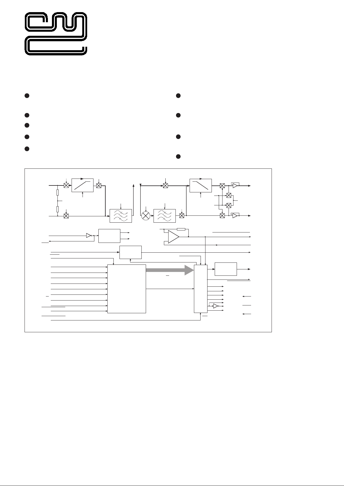
Fig.1 Internal Block Diagram
Brief Description
The FX375 is a Low-Power CMOS LSI microcircuit
designed for Tone Operated Voice Privacy in
communication systems.
This half-duplex device consists of a Fixed Frequency
Voice Band Inverter interfaced with a Continuous Tone
Controlled Squelch System (CTCSS) Encoder/
Decoder, whose allocated tone is used for voice
privacy and audio squelch operation.
Frequency Inversion is achieved by modulating the
input audio with a fixed carrier frequency to exchange
the high and low frequencies of the voice band, making
the resulting audio output unintelligible to receivers not
equipped with a compatible system.
The on-chip CTCSS Dencoder is capable of encoding
and decoding any one of 38 sub-audio tones in the
range 67.0Hz to 250.3Hz, these Xtal derived tones are
selected by a 6-bit binary word that can be loaded to
the device in either a serial or parallel format.
The Privacy function is exclusive only to units using the
same tone set, other intercepted signals remain "as
transmitted."
A 'Press to Listen' facility allows monitoring of the
channel prior to transmitting.
This device has separate, switched Rx and Tx voice,
and tone audio paths. Voice paths use switched
capacitor bandpass filters for the attenuation of subaudio tones and unwanted modulation products.
6dB/octave pre- and de-emphasis filtering in the Tx
path maintains natural sounding audio from this device
when embodied in communication transceivers.
The FX375, which is available in DIL and SMT
packages, can be simply controlled by switches, or
interfaced to a µProcessor.
External requirements are a single 5-volt supply, an
external 4.0MHz Xtal or clock input and signal coupling
components.
FX375
On-Chip Pre- and De-Emphasis
Filtering in the Tx Path
38 Programmable Tones
+ 'NoTone' Facility
Audio Path Filtering
(300Hz – 3033Hz)
Low Power 5V CMOS
Tone Operated Private/Clear
Switching
CTCSS Tone Encode/Decode
Separate Rx/Tx Speech Paths
Fixed Frequency Speech Inversion
µP Compatible Interface with Serial
or Parallel Control Loading
Tx AUDIO OUTPUT
Rx AUDIO OUTPUT
BIAS
Rx
Tx
BIAS
Rx
Tx
Tx
PRIVATE
CLEAR
6dB/OCTAVE
– 6dB/OCTAVE
Tx AUDIO INPUT
Rx AUDIO INPUT
FILTER
OUTPUT
BALANCED
MODULATOR
INPUT
f
CLK2
f
CARRIER
f
EMPH
f
EMPH
f
CLK1
Rx TONE DETECT OUTPUT
Rx TONE DECODER OUTPUT
CONTROL
PRIVATE ENABLE
LOGIC
Rx PATH
Tx PATH
PRIVATE
TX
TONE
OUTPUT
–
+
CTCSS
TONE
DETECT
HYSTERESIS
REFERENCE
LOAD/LATCH
f
CARRIER
f
CLK1
f
CLK2
LD5LD
0
XTAL
Rx TONE INPUT
Rx/Tx
CONTROL
PRESS TO LISTEN
V
SS
V
DD
V
BIAS
PTL
DECODE COMPARATOR INPUT
3333Hz
D INPUT
0
D INPUT
1
D or SERIAL CLOCK INPUT
2
D or SERIAL DATA INPUT
3
D or SERIAL ENABLE 2
4
D or SERIAL ENABLE 1
5
8-BIT
SHIFT
REGISTER
AND
LATCHES
XTAL
3333Hz
FILTERS
f
EMPH
CLOCKS
NOTONE OUTPUT
Features
Page 2
2
Pin Number Function
FX375J
FX375LH
1
2
3
4
5
6
7
8
9
10
11
12
13
14
Xtal/Clock: The input to the clock oscillator inverter. An external 4MHz Xtal or clock
input is to be applied at this pin. See Figure 2.
Xtal: The 4MHz output of the clock oscillator inverter. See Figure 2.
Load/Latch: This input regulates the operation of the eight input latches : D0, D1, D2,
D3, D4, D5, Rx/Tx and Private Enable for both parallel and serial input load modes.
Rx/Tx and Private Enable inputs can be used independently in either mode by the use
of Load/Latch and Control inputs configured as shown in Table 3, the data format
(D0 – D5), remains as set. This input has an internal 1MΩ pullup resistor.
D5 – (Serial Enable 1) :
D
4
– (Serial Enable 2) :
D3 – (Serial Data Input) :
D2 – (Serial Clock Input) :
D
1
D
0
Rx Tone Decode Output : The output of the decode comparator. In Rx a logic '0'
indicates 'CTCSS tone decoded' above the internal reference level, or Notone
programmed. This action internally enables the Rx audio path and Frequency Inversion
function (when applicable) as shown in Table 1. In Tx this output is a logic '1'.
Decode Comparator Input : A logic '1' at this pin, in Rx, is compared internally with a
fixed reference level, a more positive input value will produce a logic '0' at the Rx Tone
Decode Output. This input should be externally connected to the Rx Tone Detect
Output via external integrator components C7, R2, R3, D1 (see Figure 2).
Rx Tone Detect Output : This output, in Rx, goes to a logic '1' when a valid,
programmed CTCSS tone is received at the Rx Tone Input. This input should be
externally connected to the Decode Comparator Input via external integrator
components C7, R2, R3, D1 (see Figure 2).
Notone Output : Outputs a logic '0' when a " Notone" CTCSS code has been
programmed . It can be used to operate squelch circuitry under receive "Notone"
conditions.
VSS : Negative supply rail (GND).
The FX375LG and LS package styles are configured as a serial-data loading device,
Parallel Programing Inputs D0, D1 and D5, and the NOTONE Output pin functions are not
available.
FX375LG
FX375LS
2
3
4
–
5
6
7
–
–
8
9
10
–
11
The Rx/Tx tone programming and function inputs.
Programmed as shown in Table 2 these inputs will select
the CTCSS tone frequency and parallel or serial loading
function. Notone, when set in receive, enables the Rx
Audio Output and forces the Rx Tone Decode Output to a
logic '0,' in transmit the Tx Tone Output is held at V
BIAS
(Notone). These inputs each have an internal 1MΩ pullup
resistor. If FX375LG or LS package styles are used Pin 5
(Serial Enable 2) should be externally connected to VSS.
Page 3
3
Pin Number Function
FX375J
FX375LH
15
16
17
18
19
20
21
22
23
24
25
26
27
28
FX375LG
FX375L
12
13
14
15
16
17
18
19
20
21
22
23
24
1
Tx Tone Output : This is the buffered, programmed CTCSS tone sinewave output in
Tx. During Rx and Notone operation this output is held at V
BIAS
. See note "g," page 7 with
reference to capacitive load limits of this output.
V
BIAS
: This bias pin is set internally to VDD/2. It must be externally decoupled using a
capacitor, C8, of 1.0µF (minimum) to VSS, see Figure 2.
Filter Output : The Input Audio Bandpass Filter output, this pin must be connected to
the Balanced Modulator Input via a capacitor, C6, and decoupled to VSS by C10, see
Figure 2.
Balanced Modulator Input : The input to the Balanced Modulator, this pin must be
connected to the Filter Output via a capacitor, C6, see Figure 2.
Rx Audio Output : Outputs the received audio from a buffered output stage and is held
at V
BIAS
when in Tx.
Tx Audio Output : The output of the audio path in the Tx mode and is held at V
BIAS
when in Rx.
Rx Audio Input : The Audio input pin for the Rx mode. Input signals should be a.c.
coupled via an external capacitor, C4, see Figure 2.
Tx Audio Input : This is the voice input pin for the Tx mode. Signals should be a.c.
coupled via an external capacitor, C3, see Figure 2.
PTL : The "Press To Listen" function input, in the receive mode a logic '0' enables the
Rx Audio Output directly, overriding tone squelch but not intercepting a private
conversation. In the transmit mode a logic '0' reverses the phase of the Tx Tone Output
for "squelch tail" reduction (see Table 1), this function, in Tx, should be accurately
applied by a timing circuit to ensure correct system operation.
Control : This input, with Load/Latch, selects the operational mode of Rx/Tx and
Private Enable functions, see Table 3.
Rx/Tx : Selects the receive or transmit mode (Rx = '1', Tx = '0') and can be loaded by
serial or parallel means, as described in Table 3.
Private Enable : This input selects either Private or Clear modes (Clear = '1',
Private ='0'), and can be loaded by serial or parallel means, as described in Table 3. In
Rx this input could be taken from the Rx Tone Decode Output. This input has an internal
1MΩ pullup resistor.
Rx Tone Input : The received tone input to the on-chip CTCSS decoder and should be
a.c. coupled via capacitor C5, see Figure 2.
V
DD
: Positive supply rail. A single +5V power supply is required.
Page 4
4
Operational Information
Component Unit Value
R
1
1M
R
2
820k
R
3
330k
C
1
33p
C
2
33p
C
3
0.1µ
C
4
0.1µ
C
5
0.1µ
C
6
1.0µ
C
7
0.1µ
C
8
1.0µ
C
9
1.0µ
C
10
1.0n
D
1
Small Signal
X
1
4MHz
C
6
C
4
C
3
C
5
DECODE COMPARATOR INPUT
Rx TONE DETECT OUTPUT
Rx TONE INPUT
Rx TONE DECODE OUTPUT
SERIAL CLOCK INPUT –
SERIAL DATA INPUT –
SERIAL ENABLE 1 –
SERIAL ENABLE 2 –
XTAL/CLOCK
FX375J
CONTROL
Tx AUDIO INPUT
Rx AUDIO INPUT
Tx AUDIO OUTPUT
Rx AUDIO OUTPUT
BALANCED MODULATOR INPUT
Tx TONE OUTPUT
V
DD
V
BIAS
C
8
C
7
R
2
D
1
D
2
D
3
LOAD/LATCH
20
15
16
17
18
19
21
22
23
24
25
26
27
28
6
1
2
3
4
5
7
8
9
10
11
12
13
14
PTL
PRIVATE ENABLE
FILTER OUTPUT
R
3
D
5
D
4
D
1
D
0
Rx/Tx
V
SS
DATA INPUTS
V
SS
C
9
C
10
Recommended Xtal Components
V
SS
XTAL/CLOCK
1
2
FX375J
C
1
C
2
XTAL
R
1
X
1
XTAL
NOTONE OUTPUT
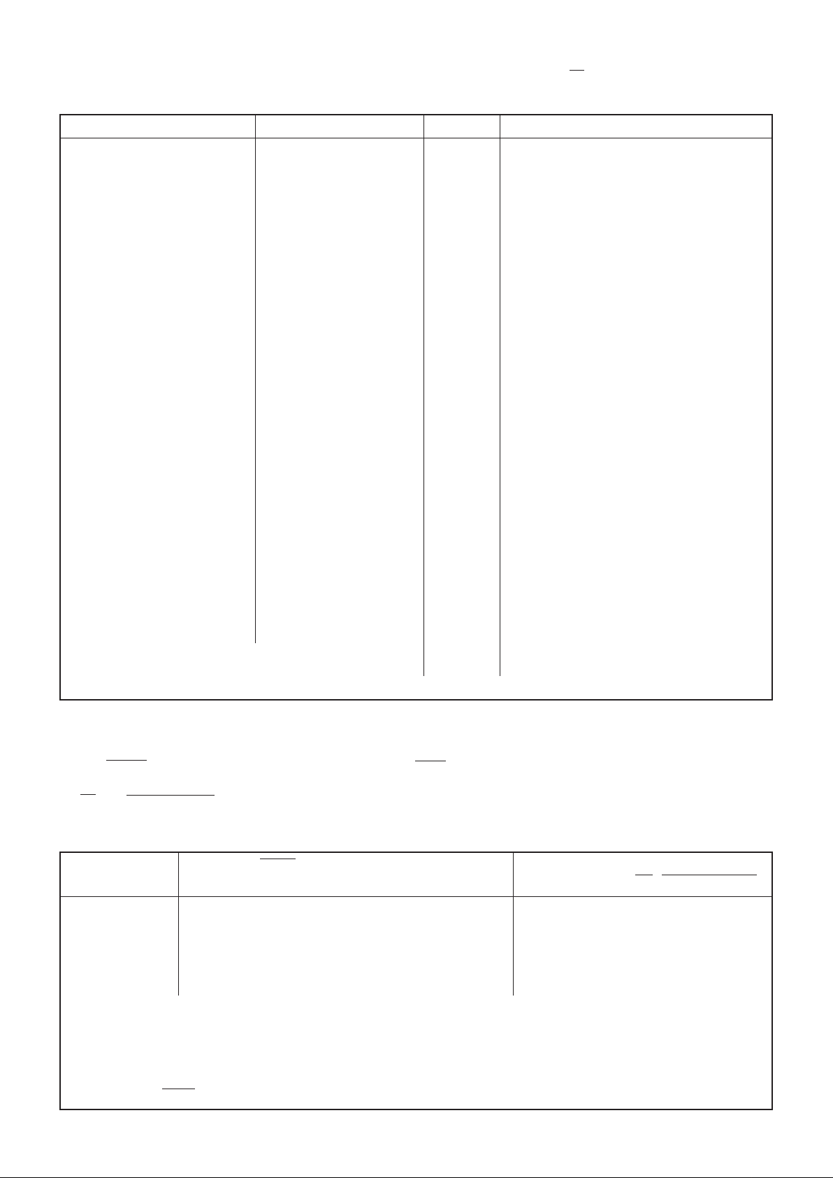
Receive Operation – (Rx/Tx = '1')
In the Rx mode Tx Tone and Tx Audio paths are held at bias.
Private Rx Tone Rx Tone Receive Signal Path
D0 – D
5
Notone Enable PTL Detect Decode State Condition
Tone 1 0 1 0 1 bias X
Tone 1 0 0 0 1 open Not Inverted
Tone 1 0 X 1 0 open Inverted
Notone 0 0 X X 0 open Not Inverted
Tone 1 1 1 0 1 bias X
Tone 1 1 0 0 1 open Not Inverted
Tone 1 1 X 1 0 open Not Inverted
Notone 0 1 X X 0 open Not Inverted
Transmit Operation – (Rx/Tx ='0')
In the Tx mode the Rx audio path is held at bias and the Rx Tone Detect output at logic '0.'
Private Transmitted Tone Transmit Signal Path
D0 – D
5
Notone Enable PTL State Phase State Condition
Tone 1 0 1 active 0° open Inverted
Tone 1 0 0 active 180° open Inverted
Notone 0 0 X bias X open Not Inverted
Tone 1 1 1 active 0° open Not Inverted
Tone 1 1 0 active 180° open Not Inverted
Notone 0 1 X bias X open Not Inverted
Notes
1. The pre- and de-emphasis circuits remain in the Transmit path during Clear and Private operation.
2. Power remains applied to the CTCSS tone decoder at all times.
3. Carrier Frequency = 3333Hz during Private operation (Tx or Rx).
4. During Clear operation the carrier frequency is turned off to reduce spurious emissions.
5. Under Rx-Notone conditions the Notone output can be used to operate squelch circuitry.
6. The functions in this table are applicable when the device is connected as recommended in Figure 2.
Table 1 Functions and Outputs
Component Tolerances
Resistors ± 10%
Capacitors ± 20%
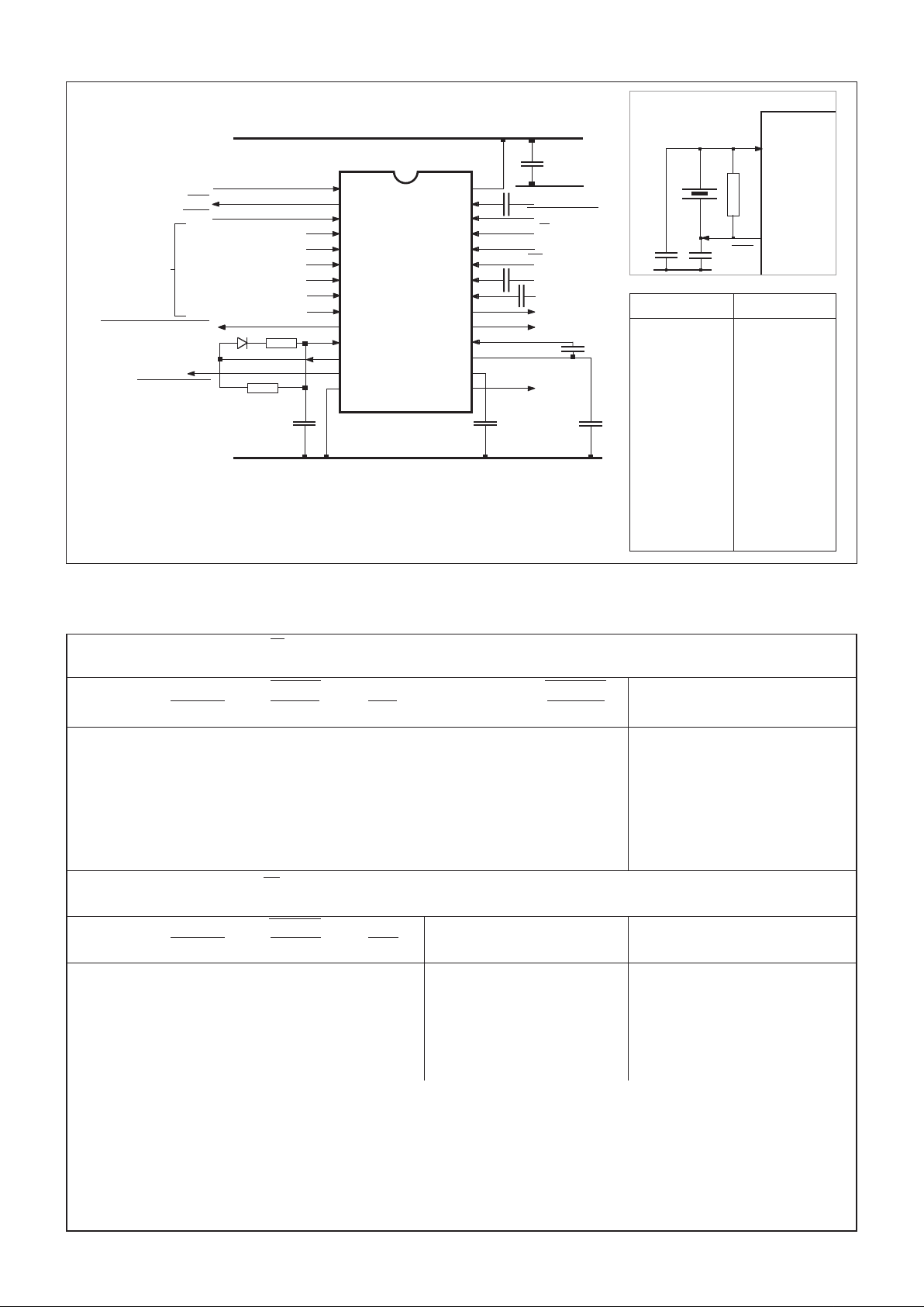
Fig.2 External Component Connections
Operational Truth Table – Table 1 (below) illustrates the output paths and logic functions of the FX375 Private
Squelch Circuit in both Receive and Transmit modes.
Page 5
5
Operational Information
The logical inputs (D0 – D5) are used to programme the FX375 tone frequency (Rx/Tx) as shown in Table 2
(below). Loading of data is carried out in either serial or parallel formats.
Nominal Frequency (Hz) FX375 Frequency (Hz) ∆fo (%) Tone Data Programme Inputs
D
0
D
1
D
2
D
3
D
4
D
5
67.0 67.05 + 0.07 111111
71.9 71.9 0 111110
74.4 74.35 - 0.07 011111
77.0 76.96 - 0.5 111100
79.7 79.77 + 0.09 101111
82.5 82.59 + 0.1 011110
85.4 85.38 - 0.2 001111
88.5 88.61 + 0.13 011100
91.5 91.58 + 0.09 110111
94.8 94.76 - 0.04 101110
97.4 97.29 - 0.11 010111
100.0 99.96 - 0.04 101100
103.5 103.43 - 0.07 001110
107.2 107.15 - 0.05 001100
110.9 110.77 - 0.12 110110
114.8 114.64 - 0.14 110100
118.8 118.8 0 010110
123.0 122.8 - 0.17 010100
127.3 127.08 - 0.17 100110
131.8 131.67 - 0.10 100100
136.5 136.61 + 0.08 000110
141.3 141.32 + 0.02 000100
146.2 146.37 + 0.12 111010
151.4 151.09 - 0.2 111000
156.7 156.88 + 0.11 011010
162.2 162.31 + 0.07 011000
167.9 168.14 + 0.14 101010
173.8 173.48 - 0.19 101000
179.9 180.5 + 0.14 001010
186.2 186.29 + 0.05 001000
192.8 192.86 + 0.03 110010
203.5 203.65 + 0.07 110000
210.7 210.17 - 0.25 010010
218.1 218.58 + 0.22 010000
225.7 226.12 + 0.18 100010
233.6 234.19 + 0.25 100000
241.8 241.08 - 0.30 000010
250.3 250.28 - 0.01 000000
Serial Input Mode X X Clk Data 0 1
Notone 000011
Table 2 Tone Programming
Load Load/Latch
and
Control Loading mode of :-
Configuration
Logic Logic
D0 – D
5
Rx/Tx, Private Enable
Parallel 1 0 Transparent Transparent
Parallel 0 0 Latched Latched
Parallel 1 1 Transparent Transparent
Parallel 0 1 Latched Transparent
Serial 0 1 Load data in Transparent
Serial 0 – 1 – 0 0 Latch data in Latched
Notes
Glossary
– Transparent Data at the device inputs acts directly.
Latched In this position data and/or functions are latched in.
'0 – 1 – 0' is a strobe pulse as shown in figures 3 and 4 (Timing).
Table 3 Load/Latch and Control Functions
Load/Latch and Control Functions – The Load/Latch function regulates the loading of the FX375 tone
frequency (D0 – D5, Table 2) in either the serial or parallel modes. The Control input enables the flexible use of the
Rx/Tx and Private Enable functions, its use is illustrated in Table 3.
Page 6
6
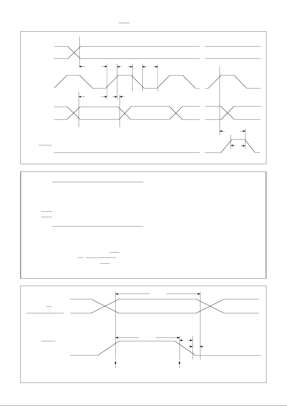
Timing Information ...... Control instructions are input to the FX375 by serial (figure 3) or parallel
(figure 4) means, using Data Inputs and Load/Latch as shown in the diagrams below.
Fig.3 Serial Load Timing
Min. Typ. Max. Unit
Serial Figure 3
Serial Mode Enable Set Up Time – (t
SMS
) 250 – – ns
Clock 'High' Pulse Width – (t
pWH
) 250 – – ns
Clock 'Low' Pulse Width – (t
pWL
) 250 – – ns
Data Set Up Time – (tDS) 150 – – ns
Data Hold Time – (tDH)50––ns
Load/Latch Set Up Time – (tLL) 250 – – ns
Load/Latch Pulse Width – (t
LLW
) 150 – – ns
Parallel Figure 4
Data Valid Time – (tVP) 200 – – ns
Load Time – (tL) 150 – – ns
Fall Time – (tF)––50ns
Data Hold Time – (tH)50––ns
Serial Loading Sequence : With Load/Latch at logic '0' serial data is loaded in the sequence :-
D5, D4, D3, D2, D1, D0, Rx/Tx, Private Enable. When these 8 bits have been clocked in on the rising clock edge,
data is latched by strobing the Load/Latch input – " 0 – 1 – 0 " (Figure 3).
Table 4 Timing
Fig.4 Parallel Load Timing
LOAD DATA DATA LATCHED
LOAD/LATCH
t
VP
t
L
t
F
t
H
- DATA INPUTS D0 – D5
Rx/Tx
PRIVATE ENABLE
SERIAL CLOCK
SERIAL MODE
ENABLE
D
4
D
5
SERIAL DATA
INPUT
LOAD/LATCH
t
SMS
t
PWH
t
PWL
t
DS
t
DH
t
LL
t
LLW
Page 7

7
Specification
Electrical Characteristics
Absolute Maximum Ratings
Exceeding the maximum rating can result in device damage. Operation of the device outside the operating limits is
not implied.
Supply voltage - 0.3 to 7.0V
Input voltage at any pin (ref V
SS
= 0V) - 0.3 to (V
DD
+ 0.3V)
Sink/source current (supply pins) +/- 30mA
(other pins) +/- 20mA
Total device dissipation @ T
AMB
25°C 800mW Max.
Derating 10mW/°C
Operating temperature range: FX375J - 30°C to + 85°C (ceramic)
FX375LG/LS - 30°C to + 70°C (plastic)
Storage temperature range: FX375J - 55°C to + 125°C (ceramic)
FX375LG/LS - 40°C to + 85°C (plastic)
Operating Limits
All device characteristics are measured under the following conditions unless otherwise specified:
V
DD
= 5.0V, T
AMB
= 25°C, Xtal/Clock f0 = 4.0 MHz, Audio level 0dB ref: = 300mV rms.
Composite input signal = 0dB, 1kHz tone in –12dB (6kHz band limited) gaussian white noise with a –20dB CTCSS
tone.
Characteristics See Note Min. Typ. Max. Unit
Static Values
Supply Voltage 4.5 5.0 5.5 V
Supply Current :
Rx /Tx (Operating) – 8.0 – mA
Rx standby (No Decode) – 2.8 – mA
Rx only (Decoding) – 5.0 – mA
Analogue Input Impedance – 0.5 – MΩ
Analogue Output Impedance – 0.5 – kΩ
Tone Input Impedance – 1.0 – MΩ
Digital Input Impedance – 1.0 – MΩ
Input Logic '1' 3.5 – – V
Input Logic '0' – – 1.5 V
Output Logic '1' (I = 0.1mA) 4.0 – – V
Output Logic '0' (I = 0.1mA) – – 1.0 V
Dynamic Values
Maximum Input Level – + 10.5 – dB
Decoder
Tone Input Signal Level 1,4 - 20 – – dB
Response Time 1,4,6 – – 250 ms
De-response Time 1,4,6 – – 250 ms
Selectivity 4 ± 0.5 – ± 3.0 %ƒo
Encoder
Tone Output Level (relative 775mVrms) - 3.0 0 + 3.0 dB
Tone Frequency Accuracy - 0.3 – + 0.3 %ƒo
Tone Harmonic Distortion – 2.0 5.0 %
Tone Output Load Current 2 – – 5.0 mA
Output Level Variation between Tones – 0.1 – dB
Rise Time (to 90% nominal level)
(ƒo >100Hz) 5 – 15 – ms
(ƒo <100Hz) 5 – 45 – ms
Page 8

8
Specification
Frequency Characteristics
Characteristics See Note Min. Typ. Max. Unit
Rx Clear
Total Harmonic Distortion 3 – 2 5 %
Output Noise Level 7 – - 43 – dB
Passband Gain (300Hz – 3033Hz) – 0 – dB
Passband Ripple (300Hz – 3033Hz) 3 – – 3 dB
Audio Stopband Attenuation
(ƒin > 3333Hz) – 20 – dB
(ƒin > 3633Hz) – 45 – dB
(ƒin < 250Hz) – 42 – dB
Rx Invert
Carrier Frequency – 3333 – Hz
Total Harmonic Distortion 3,8 – 4 10 %
Baseband Breakthrough – - 40 – dB
Carrier Breakthrough – - 40 – dB
Output Noise Level 7 – - 37 – dB
Passband Ripple (300Hz – 3033Hz) 8 – – 5 dB
Audio Stopband Attenuation
(ƒin > 3333Hz) – 50 – dB
(ƒin > 3633Hz) – 60 – dB
(ƒin < 250Hz) – 60 – dB
Tx Clear
Total Harmonic Distortion 3 – 3 5 %
Output Noise Level 7 – - 43 – dB
Passband Gain (300Hz – 3033Hz) 3 – 0 – dB
Passband Ripple (300Hz – 3033Hz) 3 – – 4 dB
Audio Stopband Attenuation
(ƒin > 3333Hz) – 20 – dB
(ƒin > 3633Hz) – 45 – dB
(ƒin < 250Hz) – 42 – dB
Pre- and De-emphasis – – 6 dB/octave
Tx Invert
Carrier Frequency – 3333 – Hz
Total Harmonic Distortion 3,8 – 4 10 %
Baseband Breakthrough – - 40 – dB
Carrier Breakthrough – - 40 – dB
Output Noise Level 7 – - 37 – dB
Passband Ripple (300Hz – 3033Hz) 3,8 – – 5 dB
Audio Stopband Attenuation
(ƒin > 3333Hz) 8 – 50 – dB
(ƒin > 3633Hz) 8 – 60 – dB
(ƒin < 250Hz) 8 – 60 – dB
Pre- and De-emphasis – – 6 dB/octave
Notes
1. These values are obtained using the external integrator components as detailed in Figure 2.
2. An Emitter Follower output.
3. With an input signal of 1kHz @ 0dB.
4. Under Composite Signal test conditions.
5. Any programmed tone with RL = 600, CL = 15pF. Including any response to a phase reversal
instruction.
6. ƒo > 100Hz, (for 100Hz > ƒo > 67Hz : t = [100/ƒo (Hz)] x 250ms).
7. Input a.c. short circuit, audio path enabled, measured in a 30kHz bandwidth.
8. Due to frequency inversion, this figures reflects the difference from the expected ideal response.
Page 9
9
receive condition the signal path will only be inverted
when the programmed CTCSS tone is received.
Although other logic actions will enable the receive
path, privacy of the conversation is maintained at all
times.
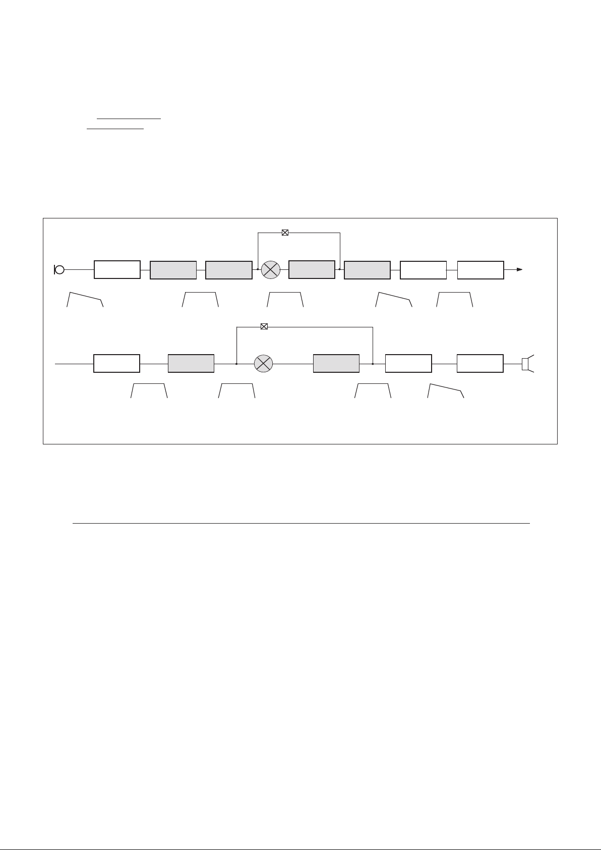
Pre- and De-emphasis (6dB/octave) filters are
included on-chip in the transmit path, so that the use of
this device will produce natural sounding audio (clear
or private modes) when installed in modern radio
communication transceivers, with or without existing
audio processing circuitry. The recommended layout is
shown in block form below.
Figure 5 shows the recommended positioning of the
Private Squelch Circuit ...... Application Notes
The FX375 Private Squelch Circuit utilizes Audio Frequency Inversion and Continuous Tone Controlled Squelch
System (CTCSS) techniques to provide secure voice communication on a common radio channel.
Clear/Private Switching is controlled by the logic state of the Private Enable input. Table 1 shows that, in the
Fig.5 The Private Squelch Circuit Installed within a Typical Audio Stage
Amplifier
Pre emphasis
Band Pass
Filter
Band Pass
Filter
De-emphasis Pre-emphasis
Modulator
To Transmitter
Stages
Demodulator
Band Pass
Filter
Band Pass
Filter
De-emphasis Amplifier
From Receiver
Stages
CLEAR
CLEAR
FX375 (shaded areas) when installed within the audio stages of a typical transceiver system. The accompanying
waveform diagrams indicate the relative "voice band amplitudes" at each stage of the receive or transmit process.
Installation Recommendations – Care should be taken on the design and layout of the printed circuit
board taking into consideration the points noted below.
(a) All external components (as recommended in
Figure 2) should be kept close to the package.
(b) Tracks should be kept short, particularly the Audio
and V
BIAS
inputs.
(c) Xtal/clock and digital tracks should be kept well
away from analogue inputs and outputs.
(d) Inputs and outputs should be screened wherever
possible.
(e) A "ground plane" connected to VSS will assist in
eliminating external pick-up on input and output
pins.
(f) It is recommended that the power supply rails have
less than 1mV rms of noise allowed.
(g) Tx Tone Output loading – Large capacitive loads
could cause this pin to oscillate. If capacitive loads
in excess of 100pF are unavoidable, a resistor of
1kΩ or greater put in series with the load should
minimise this effect.
Page 10
Package Outlines
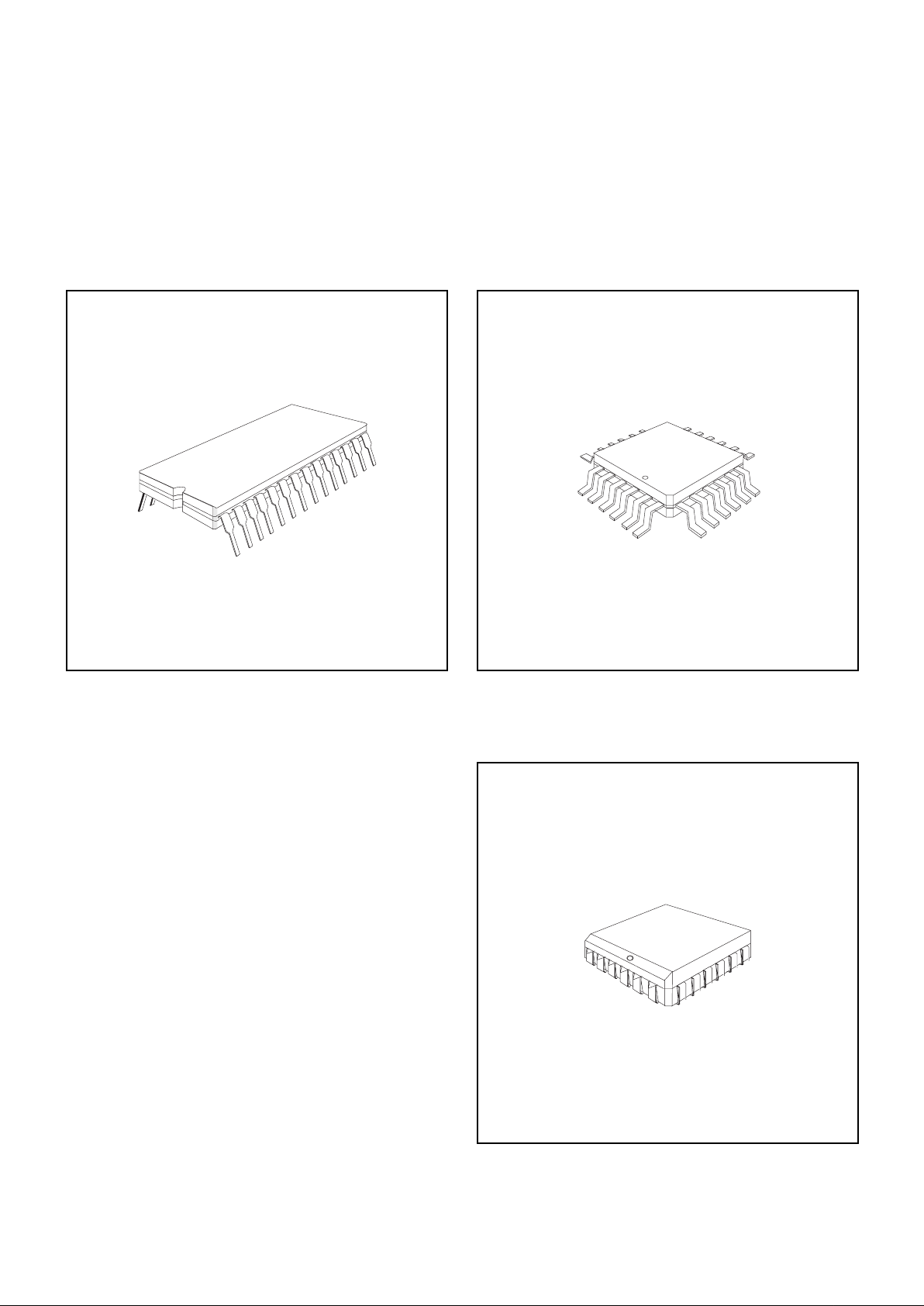
The FX375 is available in the package styles outlined
below. Mechanical package diagrams and specifications
are detailed in Section 10 of this document.
Pin 1 identification marking is shown on the relevant
diagram and pins on all package styles number
anti-clockwise when viewed from the top.
Handling Precautions
The FX375 is a CMOS LSI circuit which includes input
protection. However precautions should be taken to
prevent static discharges which may cause damage.
CML does not assume any responsibility for the use of any circuitry described. No circuit patent licences are implied
and CML reserves the right at any time without notice to change the said circuitry.
Ordering Information
FX375J 28-pin cerdip DIL (J5)
FX375LG 24-pin encapsulated bent and
cropped (L1)
FX375LS 24-lead plastic leaded chip
carrier (L2)
NOT TO SCALE
Max. Body Length 10.25mm
Max. Body Width 10.25mm
FX375LG 24-pin quad plastic encapsulated
bent and cropped (L1)
NOT TO SCALE
Max. Body Length 10.40mm
Max. Body Width 10.40mm
FX375LS 24-lead plastic leaded chip carrier
(L2)
NOT TO SCALE
Max. Body Length 37.05mm
Max. Body Width 13.36mm
FX375J 28-pin cerdip DIL (J5)
 Loading...